Direct Detection of sub-GeV Dark Matter with Semiconductor Targets
Abstract
Dark matter in the sub-GeV mass range is a theoretically motivated but largely unexplored paradigm. Such light masses are out of reach for conventional nuclear recoil direct detection experiments, but may be detected through the small ionization signals caused by dark matter-electron scattering. Semiconductors are well-studied and are particularly promising target materials because their band gaps allow for ionization signals from dark matter particles as light as a few hundred keV. Current direct detection technologies are being adapted for dark matter-electron scattering. In this paper, we provide the theoretical calculations for dark matter-electron scattering rate in semiconductors, overcoming several complications that stem from the many-body nature of the problem. We use density functional theory to numerically calculate the rates for dark matter-electron scattering in silicon and germanium, and estimate the sensitivity for upcoming experiments such as DAMIC and SuperCDMS. We find that the reach for these upcoming experiments has the potential to be orders of magnitude beyond current direct detection constraints and that sub-GeV dark matter has a sizable modulation signal. We also give the first direct detection limits on sub-GeV dark matter from its scattering off electrons in a semiconductor target (silicon) based on published results from DAMIC. We make available publicly our code, QEdark, with which we calculate our results. Our results can be used by experimental collaborations to calculate their own sensitivities based on their specific setup. The searches we propose will probe vast new regions of unexplored dark matter model and parameter space.
1 Introduction
1.1 The search for dark matter
There has been tremendous progress in the last three decades in the direct detection search for weak-scale dark matter (DM) using underground detectors. The original aim was to probe the scattering through -exchange of DM candidates with roughly weak-scale mass against nuclei [1]. Now, experiments searching for these DM-induced nuclear recoils [2, 3, 4] are sensitive to scattering cross sections many orders of magnitude below the -exchange cross section, for candidates in the (10 GeV–10 TeV) mass range. The motivation behind this incredible experimental achievement has been the theoretically appealing, and dominant, Weakly Interacting Massive Particle (WIMP) paradigm: DM as a weak-scale thermal relic associated with new physics that solves the hierarchy problem. However, the era of this paradigm’s preeminence appears to be ending due to both the lack of a DM discovery, which excludes significant regions of WIMP parameter space, and the absence of non-Standard Model (SM) physics at colliders, which has undermined the theoretical motivation behind it. More importantly, several other theoretically motivated candidates exist for resolving this great mystery of particle physics.
Motivated particle-DM candidates have been proposed over a vast range of masses, from ultra-light bosonic fields such as a QCD axion [5, 6, 7], to non-thermal GUT-scale relics [8]. While these have inspired a diverse array of experimental searches, techniques for probing them are far less developed than the WIMP search program. One well-motivated candidate that has received increased attention recently and is the focus of this paper is light dark matter (LDM), with DM masses in the MeV to GeV range. LDM is often motivated by production mechanisms that go beyond the standard freeze-out and may be found in several frameworks in which the sub-GeV mass scale arises naturally. In addition, the origin for the DM relic density can be naturally addressed by several mechanisms that suggest that LDM interacts with SM particles via, for example, an exchange of a light “dark photon”, an axion, or through an electromagnetic dipole moment. There is a large range of parameter space of such models that evades both laboratory and astrophysical bounds [9, 10, 11, 12, 13, 14, 15, 16, 17, 18, 19, 20, 21, 22, 23, 24, 25, 26, 27, 28, 29, 30].
Investigating LDM is an important and natural direction to pursue in the DM search effort. An essential part of this pursuit is extending direct detection searches to this low mass range. Several possible ways to do this were described in [9]. Fortunately, much of the impressive technology being developed for the Weak-scale direct detection program can be readily adapted to search for LDM. An example of this was described in [31], obtaining the first direct detection limits on DM with masses as low as a few MeV using published XENON10 data. In this work, we study in detail the even more promising possibility of semiconductor-based LDM searches, significantly expanding the preliminary work done in [9]. Other, complementary techniques to search for LDM have been discussed in [32, 33, 34, 35, 36, 37, 38, 39, 40, 41, 42, 43, 44, 45, 46, 47, 48, 49, 50, 51, 52, 53, 54, 55, 56, 57, 58, 59, 60, 61].
1.2 Direct detection of sub-GeV dark matter
Current direct detection experiments are limited to probing DM masses above a few GeV due to the high energy thresholds required for detecting nuclear recoils. The challenge in probing lower DM masses is twofold: for lower masses, not only is the total kinetic energy of the DM particle decreased, but so is the fraction of energy that is transferred to the nucleus. As a result, the energy of the nuclear recoils is much lower and one must drastically reduce the threshold energies to detect it. This is an experimentally challenging task, although it may be possible to probe masses down to a few hundred MeV, see [62, 63]. Instead, as discussed in [9], scattering channels other than elastic nuclear recoil are likely to be far more fruitful.
A very promising avenue is to search for the small ionization signals caused directly by DM-electron scattering. The lightness of the electron and the inelastic nature of the DM-electron scattering process allow DM particles to transfer a large fraction of their kinetic energy to the electron when they scatter, enabling DM as light as 1 MeV to cause an ionization signal. Furthermore, detecting small ionization signals is already a well-developed part of direct detection technology. In fact, the XENON10 experiment was already sensitive to the ionization of a single electron [64], and results of a short single-electron-sensitive run [65] were used in [31] to place direct detection bounds on DM with masses as low as a few MeV. This serves as a proof-of-principle, motivating dedicated LDM searches in other dual-phase noble liquid experiments such as XENON100 and LUX. However, semiconductor targets have the potential to probe even smaller cross sections. In semiconductors such as silicon or germanium, the band gap (the threshold to “ionize” an electron by exciting it from a valence band to a conduction band) is 1 eV – a factor of 10 to 20 times lower than the ionization threshold in liquid xenon. The consequences of this lower energy threshold are significant. Not only could this allow sensitivity to DM down to masses below an MeV, but it would also mean a substantial increase in event rate for all DM masses [9, 25]. The reason for this is that, given the characteristic velocities of DM particles and electrons, 1 eV recoil energies are typical, while recoil energies of 10 eV require velocities that are only found on the tails of the DM and electron velocity distributions. Moreover, although the background that causes an ionization signal at such low energies is still poorly understood, it is reasonable to expect that background event rates in semiconductors may be significantly lower than in xenon-based detectors [66] (especially since they may be operated cryogenically)11 1 Unlike for traditional WIMP searches, nuclear recoils are not an important background for our electron recoil signal as their rates are expected to be much lower than background-induced electron recoils.. There is currently an active program in, for example, both the SuperCDMS and DAMIC collaborations to develop germanium- and silicon-based detectors that are sensitive to single electron-hole pairs [66, 67], enabling a leap forward in LDM detection.
This developing experimental program presents a new theoretical challenge: the calculation of the expected signal rate. Unlike for elastic nuclear recoils, this calculation is highly non-trivial. In this paper, we tackle this calculation head on and present detailed new results for germanium and silicon targets.
1.3 The challenge of calculating event rates
Several factors complicate the calculation of DM-electron scattering rates. Bound electrons in dense media have a) typical speeds of order or greater, much faster than DM particles (with ), b) indefinite momentum, with even very large momenta having non-zero probability, and c) a complicated structure of energy-levels. This greatly modifies the scattering kinematics and breaks the simple link between momentum transfer and energy deposition. As we discuss in more detail below, event rates can be highly sensitive to the energy-level structure and the tails of the electrons’ momentum distributions. In addition, the quantum nature of both the initial and final electron states is important, and they cannot be correctly treated classically. As a result, approximate calculations which do not fully account for these details may not give accurate results. This becomes even more important for the large energy depositions, well above (eV), since these rely on the tails of the electron’s momentum distribution. Once correctly calculated, the effect of all these complications can be completely encoded in an atomic form factor [9]. This function is different for each specific target material, but is independent of the DM model. Once it is known, event rates can be calculated relatively simply.
When the target is an isolated noble gas atom, the combination of spherical symmetry and previously-compiled bound-state electron wavefunctions makes calculation of the ionization form factor relatively straightforward. Refs [9, 31] used this as an approximation for the form factor of a liquid xenon target. However, calculating the form factor for a crystal target (such as a semiconductor) is far more challenging. A periodic crystal lattice is a complex multi-body system, with outer-shell (valence) electrons delocalized and occupying a complicated energy band-structure. Accurate wavefunctions of the valence electrons cannot be found analytically, but must be computed numerically with an expansion in a discrete set of plane waves22 2 Note that inner-shell (core) electrons, which are important in some cases, are more localized so that their wavefunctions are closer to those computed assuming an isolated atom.. Taking this approach, a first calculation was done in [9], assuming a single-electron threshold in a germanium target. A second approach was taken in [25], which succeeded in simplifying the calculation until it was analytically tractable. However, the approximations required for this were so extensive that the result might be considered only as an order-of-magnitude estimate. A third, semi-analytic approach was taken in [68] (see “Note Added”), where numerical bound-state wavefunctions for free germanium and silicon atoms are used and the outgoing electrons are described by plane waves. The latter approach gives answers much closer to our full numerical calculation, but important differences remain.
1.4 Overview of the paper
In this paper, we present the results of a detailed numerical computation of DM-electron scattering rates in germanium and silicon targets as a function of the electron recoil energy. This significantly expands on the previous calculation in [9]. Higher recoil energies for the scattered electron allow a larger number of additional electron-hole pairs to be promoted via secondary scattering. Using a semi-empirical understanding of these secondary scattering processes, we convert our calculated differential event rate to an estimated event rate as a function of the number of observed electron-hole pairs. These results will allow several experimental collaborations, such as DAMIC and SuperCDMS, to calculate their projected sensitivity to the DM-electron scattering cross-section, given their specific experimental setups and thresholds. It will also allow them to derive limits on this cross section in the absence of a signal, or the preferred cross section value should there be a signal, in forthcoming data. Achieving low ionization thresholds could allow these experiments to probe large regions of LDM parameter space in the near future, as illustrated in Fig. 1.
In §2, we briefly discuss the direct detection prospects for a few popular LDM models. We will see that the upcoming generation of experiments with semiconductor targets play an essential role in testing these models. In §3, we outline how to calculate the rate for DM to scatter off bound electrons. We provide an intuitive understanding of the scattering kinematics. Our discussion is general and applicable to both electrons bound to (free) atoms as well as electrons in semiconductor targets. The details of this calculation as well as comprehensive formulas are contained in Appendix A, significantly expanding on the information contained in [9, 31]. We then focus on semiconductor targets, and describe the numerical computation of the scattering rates in §4. We describe our code QEdark, which is an additional module to the publicly available code Quantum ESPRESSO [69]. The latter calculates the band structure and all electron wavefunctions using density functional theory (DFT) and pseudopotentials, two established condensed matter computational tools, to calculate the Bloch wavefunction coefficients for the initial and final state electrons. In QEdark, we use this information to calculate the crystal form factor for DM-electron scattering as well as the scattering rates. QEdark and the crystal form factors will be publicly available at this link. In §5, we discuss the conversion from the energy of the primary scattered electron to the size of the final ionization signal. We present a conversion formula and discuss the uncertainty associated with it. In §6, we present the results of our computation, showing the cross-section sensitivity as a function of detector threshold, as well as the potential discovery reach using annual modulation. We also provide detailed sensitivity estimates for two representative, near-term experiments that may soon reach the required sensitivity to detect LDM, namely DAMIC and SuperCDMS. We conclude in §7. The appendices contain additional technical details: Appendix A provides a detailed derivation of the formulae for the scattering rate and crystal form-factor, Appendix B describes our choice of local DM velocity distribution, Appendix C discusses the convergence of our numerical results, Appendix D studies the effects of inner-shell electrons on the overall scattering rate, Appendix E presents details of the systematic study of secondary interactions, and Appendix F gives a brief review of DFT and pseudopotentials.
2 Models of Light Dark Matter
Theories of LDM have been receiving increased attention in recent years. Here we illustrate with just a few benchmark LDM models how the upcoming generation of experiments with semiconductor targets, including SuperCDMS and DAMIC, play an essential role in the search for LDM. Classes of models that are probed by LDM direct detection include DM that scatters through a dark-photon mediator or through a dipole moment interaction. We focus on DM coupled to a dark photon, leaving a discussion of dipole moment interactions [70, 25], the SIMP [29, 30], and other models that can be constrained by electron recoils to an upcoming publication [71].
For illustration, we consider models of LDM based on the vector-portal, in which the dark sector (and the DM particle, ) communicates with the SM through a gauge boson . The is kinetically mixed with the SM hypercharge via the interaction
| (1) |
causing it to couple dominantly to electrically charged particles at low energies. Here is the kinetic mixing parameter, is the Weinberg mixing angle, and () is the () field strength.
DM particles can scatter off electrons in direct-detection experiments through exchange. In the notation of §3.2 below, the DM-electron reference cross section is given by
| (2) |
where is the DM-electron reduced mass and (with the gauge coupling). We note that this expression is the same for DM that is a complex scalar or a fermion. The corresponding DM form factor is
| (3) |
where is the momentum transfer between the DM and electron.
In Fig. 2, we illustrate the parameter spaces of both the and regimes, taking the fermionic and complex-scalar cases separately for the former. We study three cases, which highlight different possible production mechanisms, and show the interplay between different experimental probes.
- (i)
Freeze-out via the vector portal: complex scalar LDM
We consider the phenomenologically interesting and predictive region , corresponding to . Annihilation to SM particles occurs via an off-shell (). This process is -wave suppressed, allowing the DM abundance to be set by thermal freeze-out while evading constraints from the cosmic microwave background (CMB), e.g. [72, 73], and from gamma-rays in the Milky-Way halo [74]. We show the parameter space for this scenario in Fig. 2 (top left), taking for concreteness. The thick blue curve shows the cross-section for which the correct relic abundance is obtained from freeze-out [73] (this is largely insensitive to the specific choice of ). Above this line, an asymmetric DM component may complete the DM abundance. Below it, the abundance is naively too large, but this region may be viable with alternate hidden-sector freeze-out channels. We also show various constraints on this model. The black curve labelled “XENON10” shows the electron-recoil DM constraint set with XENON10 data [31]. The black curve labelled “Current NR Constraints” shows constraints from conventional nuclear-recoil searches from [3, 75, 76]. Some measurements only constrain as a function of . Among these, we only show the strongest constraints, which are a BaBar search for [49, 51, 52] as well as electroweak precision tests (EWPT) [77, 78]; however, to guide the eye, we also show the “favored” -region for which the can explain the discrepancy between the measurement and SM prediction for the muon anomalous magnetic moment, [79]. We translate these into the versus plane by using the constraint on from either perturbativity [80] or self-interactions [22]. For these we require that is less than 1.0 and small enough so that cm2/g for clusters [81]. A second set of constraints bound some combination of , , and : the electron beam-dump E137 [82, 57] and the proton beam-dump LSND [83, 84, 60]. We again use the constraint on from self-interactions and perturbativity to translate these into the versus plane. We also show a rough bound on , see [53, 54, 73]; the presence of additional relativistic degrees of freedom could allow this bound to be evaded. For a complementary representation of this parameter space see [59]. - (ii)
Freeze-out via the vector portal: Dirac fermion LDM
In Fig. 2 (top right), we consider the same scenario as in (i) but take to be a Dirac fermion. This also corresponds to . The main difference between this scenario and (i) is that the annihilation cross section is now -wave, so that constraints from the CMB preclude the abundance being set by freeze out. Instead, we assume the abundance to be asymmetric [85, 86, 87], and require the symmetric component to be small enough after freeze-out to avoid the CMB bounds [20]. This provides a lower bound on the annihilation cross-section and thus on , shown with a black solid line. As before, this lower bound is model-dependent and can be evaded with additional annihilation channels. The other constraints are similar. - (iii)
Freeze-in via the vector portal
In Fig. 2 (bottom), we consider an ultra-light mediator (), corresponding to . Here the couplings are so small that the DM would never have thermalized with the SM sector. The abundance can receive an irreducible “freeze-in” [88] contribution from annihilation of SM particles to as well as -boson decays to , computed in [9] (see also [24]). The parameters required for the abundance again uniquely constrain versus , as shown by the thick blue curve. In addition to the XENON10 electron-recoil constraint [31], we also show the bounds from conventional nuclear-recoil searches. The nuclear recoil cross-section, , can be related to the electron recoil cross-section by(4) where the target nucleus has mass and atomic number , is the nuclear recoil energy, and , is relative velocity of the DM, and is the inverse mean speed defined in Appendix B. Since this recoil spectrum is peaked towards low energies more than for a contact interaction, determining accurate DM constraints requires a careful analysis of the experimental data. We place approximate bounds from “CDMSLite” [89] and LUX [3] results, taking the former to have 6.2 kg-days germanium exposure, a 0.84 keV threshold, 100% signal efficiency and 10 observed events, and taking the latter to have 10 tonne-days xenon exposure, a 5 keV threshold, 50% signal efficiency and 0 observed events. Due to the smallness of the couplings, the other constraints seen in the previous scenarios are absent in this one. Instead, we include various astrophysical constraints on millicharged particles, which are also applicable for DM coupled to an ultralight [90].
In each of the figures in Fig. 2 we show the prospects for DAMIC (100 g-years, silicon target, 2-electron threshold) and SuperCDMS (10 kg-years, silicon, 1-electron threshold), discussed in §6.5. We note that a magnetic-dipole-moment interaction would also give , while an electric-dipole-moment interaction would give . We see that these models above all have concrete predictions that the upcoming generation of direct detection experiments can test.
3 Direct detection of dark matter by electron scattering in semiconductors
In this section, we review the theory of DM scattering with bound electrons. We begin in §3.1 by considering the simple kinematics of LDM scattering with both nucleons and electrons. This makes clear the motivation for using electron recoils to probe LDM. The discussion also shows that the DM-electron scattering rate is expected to be sensitive to the details of electron binding in the target, especially for higher energy/ionization thresholds. A consequence of this is that to calculate accurate scattering rates, detailed modeling of the electronic structure of the target material is required, involving knowledge of the wavefunctions of all accessible occupied and unoccupied electron levels.
In §3.2, we summarize how this scattering-rate calculation is formulated, with a focus on the case of semiconductor targets. The key results are Eqs. (17) and (21). The former gives the differential scattering rate in terms of the DM model, the DM velocity profile, and crystal form factor. The latter gives the crystal form-factor, which encodes all the relevant electron binding effects for a given target material. This reviews and extends the discussion from Ref. [9]. In Appendix A, we provide a full derivation of all the results given here. For the interested reader, in Appendix A.3 we present a derivation of the ionization rate in free atomic targets, as is relevant for xenon targets and which was used in Refs. [9, 31].
3.1 Kinematics of dark matter-electron scattering
Conventional DM direct detection experiments assume that the DM particle scatters elastically off a target nucleus. This recoiling nucleus then collides with the surrounding matter within the detector, giving off energy in the form of heat, phonons, ionized electrons, scintillation photons, etc, depending on the detector material. However, if the DM particle is light, the momentum transfer, , between the DM and the target nucleus is small and may not provide enough energy for the recoil of the nucleus to be detected. We can see this through the following argument. The energy of the recoiling nucleus in nuclear scattering is
| (5) |
For the scaling in the last step of this equation, we have taken the typical DM speed to be km/s , and assumed . For GeV, we find keV. However, if we consider lighter DM masses, such as MeV, the recoil energy drops to eV, which is well below the detection thresholds of current direct detection experiments (e.g. eVNR for CDMSlite [89] and keVNR for LUX [3]). Note that the energy of the recoiling nucleus is also not efficiently transferred to electrons, and so is not nearly large enough to ionize or excite even a single electron; it is also well below current phonon detection thresholds. As a result, DM masses below a few hundred MeV escape detection no matter how large their cross section.
Now consider a DM particle colliding directly with a bound electron, exciting it to a higher energy level or an unbound state, as illustrated in Fig. 3. The kinematics are very different from those of a nuclear recoil. Firstly, being in a bound state, the electron does not have definite momentum – in fact it may have arbitrarily high momentum (albeit with low probability). This breaks the direct relation between recoil energy and momentum transfer given in Eq. (5). The energy transferred to the electron, , can still be related to the momentum lost by the DM, , via energy conservation:
| (6) |
Here the term accounts for the fact that the whole atom also recoils. In practice this term is small, which also allows us to replace with . We thus define
| (7) |
as the energy transferred to the electron.33 3 We emphasize that is the energy transferred to the electron, not its kinetic energy. Some of this energy goes to overcoming the binding energy. As we will discuss further in §5, in semiconductors the remaining energy is rapidly redistributed by secondary scattering processes, which can produce further electron-hole pairs. Since an arbitrary-size momentum transfer is now possible, the largest allowed energy transfer is found by maximizing with respect to , giving
| (8) |
This shows that all the kinetic energy in the DM-atom collision is (in principle) available to excite the electron. For a semiconductor with an (eV) bandgap, ionization can be caused by DM as light as (MeV).
What is the likelihood of actually obtaining a large enough to excite the electron? This brings us to the second major difference compared to DM-nuclear scattering: the electron is both the lightest and fastest particle in the problem. The typical velocity of a bound electron is , where is 1 for outer shell electrons and larger for inner shells. This is much greater than the typical DM velocity of . The typical size of the momentum transfer is therefore set by the electron’s momentum,
| (9) |
where is the relative velocity between the DM and electron.
Returning to Eq. (6), the first term on the right dominates as long as is well above the bound in Eq. (8). This gives a formula for the minimum momentum transfer required to obtain an energy :
| (10) |
This scaling suggests that the typical available momentum is enough to cause a transition of just a few eV, such as for an electron being excited just across the germanium or silicon bandgap. Exciting a more energetic transition will require a momentum out on the tail of the electron’s momentum-space wavefunction (or probing the tail of the DM velocity distribution), and its probability will be correspondingly suppressed (as can be seen clearly in Fig. 5 below, which we will discuss in §6.1). Ionization of a xenon atom, requiring 10 eV energy, falls into the second category, as do most possible transitions to the conduction band in germanium or silicon.
From this argument we expect the rate of DM-electron scattering to be sensitive to the precise forms of the electron energy levels and wavefunctions in the target. The computation we present below is designed to address this sensitivity by modeling in detail the electronic structure in germanium and silicon crystals. A corollary of this argument is that, given the -dependence in Eq. (10), the rate should also be sensitive to the DM velocity profile. As this varies over the year, we expect a significant annual modulation in the signal size, a potentially crucial test of the DM origin of a signal. We discuss the expected annual modulation in §6.4.
3.2 Calculating excitation rates
3.2.1 General formulation for dark matter-induced electron transitions
If a DM particle scatters with an electron in a stationary bound state such as in an atom, it can excite the electron from an initial energy level 1 to an excited energy level 2 by transferring energy and momentum . The cross section for this process takes quite a different form to the free elastic scattering cross section.
If is the matrix element for free elastic scattering of a DM particle and an electron, then we parametrize the underlying DM–electron coupling using the following definitions [9]:
| (11) | |||
| (12) |
where is the absolute square of , averaged over initial and summed over final particle spins. The DM form factor, , gives the momentum-transfer dependence of the interaction – for example, results from a point-like interaction induced by the exchange of a heavy vector mediator or magnetic dipole moment coupling, for an electric dipole moment coupling, and for exchange of a massless or ultra-light vector mediator (see §2). parameterizes the strength of the interaction, and in the case of is equal to the cross section for free elastic scattering. All sensitivity estimates or constraints on LDM will be given for , which plays the analogous role to , the DM-nucleon scattering cross section, in (WIMP) DM scattering with nuclei.
With these definitions, the cross section for a DM particle to excite an electron from level 1 to level 2 can be written as (see Appendix A.1)
| (13) |
where is the atomic form factor for the excitation. It is given by
| (14) |
where and are the normalized wavefunctions of the initial and final electron levels. We now apply this general result to the special case of electrons in a periodic crystal lattice, such as a semiconductor.
3.2.2 Excitation rate in a semiconductor crystal
The periodic lattice of a semiconductor crystal has a continuum of electron energy levels, forming a complicated band structure (see Fig. 4). A small energy gap separates the occupied valence bands from the unoccupied conduction bands; exciting electrons across this bandgap creates mobile electron-hole pairs, which can be manipulated and detected. In order to perform practical calculations for this system, the true multi-body electron wavefunction must be replaced with a product of single-particle wavefunctions (this is a well-understood procedure, which we discuss further in §4). Once found, these single-particle wavefunctions can be used in Eqs. (13) and (14), giving the cross-section to excite an electron between specific energy levels. To find the total rate, these cross sections are integrated over initial and final electron levels, and over the DM velocity distribution.
DM halo dependence.
Neither the electron band structure, nor the electron wavefunctions, nor the DM velocity distribution are spherically symmetric. As noted in [9], the excitation rate will therefore depend on the orientation of the crystal with respect to the galaxy, an effect which may be extremely useful in verifying the DM origin of a signal. Here, however, we sidestep this complication by approximating the DM velocity distribution as being a spherically symmetric function . All the relevant information about the DM velocity profile can then be encoded in the function (see Appendix A.2), defined as
| (15) |
where is the Heaviside step function.
When calculating rates, we assume a Maxwell-Boltzmann distribution with a sharp cutoff (we describe this in more detail, and give analytic formulas for , in Appendix B). The requirement of energy conservation is captured by , the minimum speed a DM particle requires in order for the electron to gain an energy with momentum transfer (note that was also denoted as in §3.1). This is given by
| (16) |
Differential rate.
As we show in Appendix A.4, the differential electron scattering rate in a semiconductor target (with the approximation of a spherically symmetric DM velocity distribution) can be written as
| (17) |
where GeV/cm3 is the local DM density, is the total energy deposited, and is the number of unit cells in the crystal target. ( for germanium, and for silicon.) We have written this in such a way that the first line gives a rough estimate of the rate, about 29 (11) events/kg/day for silicon (germanium) for GeV/cm3, MeV, and cm2 (the current limit from XENON10 [31]), while every factor in the second line is a roughly number for the preferred values of and .
All the necessary details of the target’s electronic structure are contained in the dimensionless crystal form factor, , which is a property purely of the target material and is independent of any DM physics. The computation of this form factor is one of the main results of this paper.
Crystal form factor.
In the periodic lattice of a semiconductor crystal, each electron energy level is labelled by a continuous wavevector in the first Brillouin Zone (BZ), and by a discrete band index . The wavefunctions of these states can be written in Bloch form,
| (18) |
where the ’s are the reciprocal lattice vectors. Here is the volume of the crystal, and the wavefunctions are taken to be unit-normalized, so that
| (19) |
Using this form for the wavefunctions, we can define the form factor for excitation from valence level to conduction level ,
| (20) |
The crystal form factor required in Eq. (17) is then given by
| (21) |
(See Appendix A.4 for the derivation.) The band index is summed over the filled energy bands, while is summed over unfilled bands, and the momentum integrals are over the 1st BZ. is the energy of level , and is the volume of the unit cell. The numerator in the first factor has units of energy, with value eV for germanium and 2.0 eV for silicon. The crystal form factor can be computed numerically using established solid-state computational techniques. Once it is known, it can be used to find event rates for any DM model and halo profile, using Eq. (17), along with Eqs. (11), (12), (15), and (16). We now turn to our own numerical evaluation of the crystal form factor.
4 Numerical computation of the form factor
Our aim is to compute the crystal form factor, given by Eq. (21), for silicon and germanium targets with low energy thresholds ( eV). Once these are found, it is possible to calculate scattering rates for any DM model. Calculating the form factor requires knowledge of the electron wavefunction coefficients for all energetically accessible electron levels. To calculate these coefficients, we utilize the “plane wave self-consistent field” (PWscf) code within the Quantum ESPRESSO [69] package, based on the formalism of DFT. We then input these into our own postprocessing code, QEdark, to calculate the form factors. In this section, we summarize the key conceptual and numerical details of our computation. We provide a review of DFT in Appendix F, detail the approximations used in the computation of the wavefunctions, and lay out the numerical methods. In Appendix C, we discuss the convergence of our computation.
4.1 Computational framework
It is impossible in practice to obtain the exact many-electron wavefunctions that describe interacting electrons in a many-body system such as a crystal. Instead, several methods exist to obtain excellent numerical approximations to these wavefunctions. We use DFT, which reformulates the interacting quantum many-body problem in terms of functionals of the particle density . For the case of electrons, the Hohenberg-Kohn theorems [91] imply that all properties of the interacting system are determined once the ground-state electron density is known. In order to obtain the ground-state density, we use the Kohn-Sham method [92] to map the system of interacting electrons into a system of independent electrons under the presence of an auxiliary potential that produces the same ground-state density. After this mapping, one has to solve the much simpler non-interacting electron system in order to obtain the ground-state energy and electron density.
The mapping from an interacting to a non-interacting many-body system comes at the expense of having to use an approximate auxiliary potential. Typically this potential is split into the mean-field Hartree potential and an exchange-correlation potential. The latter captures the quantum mechanical effect of having identical electrons and also attempts to capture the correlation energy among the interacting electrons. The exchange-correlation potential is not known exactly and needs to be approximated. We use the Perdew-Burke-Ernzerhof (PBE) functional [93], which belongs to the class of the Generalized Gradient Approximations (GGA). We discuss this further in Appendix F.
Both silicon and germanium have a diamond lattice structure that contains two atoms in the unit cell. There are two s-shell and two p-shell valence electrons per atom (3s and 3p (2s and 2p) for germanium (silicon)), which makes a total of 8 electrons per cell. This translates to 4 valence bands, since each band is doubly degenerate in electron spin. In silicon, the core electrons have binding energies of 100 eV and above, and so are irrelevant for the energies we consider here. One must take more care with germanium, since the electrons have binding energies of 30 eV, and so can be relevant for the higher energy thresholds we consider here.44 4 We thank the authors of [68] for discussions regarding this point. In the computation, energetically-inaccessible core electrons can be replaced with a pseudopotential, which increases the computational efficiency by reducing the number of initial states required, and by reducing the resolution needed to describe the wavefunctions. We use ultrasoft pseudopotentials [94] in place of all but the outer two s-shell and two p-shell valence electrons. For germanium, we also use a pseudopotential that allows us to treat the electrons as valence states. As a result, the computational cost for germanium is slightly higher than that of silicon. We use an empirical “scissor correction” approach [95, 96] to set the band gap to eV for silicon and eV for germanium [97].55 5 These values are measured at 300 K, and change by 5–10% as the temperature approaches 0 K [94]. The effect of this on our results is a few percent and therefore negligible.
4.2 Discretization procedure and cutoff choices
In order to obtain the crystal form factor with a finite computation, several modifications must be made to Eq. (21):
- •
Binning in and . The form factor must be evaluated for finite grid of - and -values. We do this by averaging over bins of equal width in and :
(22) Here is the central value of the nth bin, and is the central value of the mth energy bin, and and are the widths of the bins. We use 500 -bins with eV and 900 -bins with .
- •
Discretization in . The continuum of -values in each energy band must be replaced with a discrete mesh of representative -points. The -integrals in Eq. (21) are then replaced with finite sums:
(23) Here is the volume of the Brillouin Zone, is the volume of the crystal’s unit cell, and are the weightings of the k-points, with (following the convention of Quantum ESPRESSO). We use a uniform -point mesh.
- •
Cutoff in , . The wavefunctions are expanded in a finite size plane-wave basis whose reciprocal lattice vectors satisfy the “kinetic energy” cutoff (really a cutoff in the space of -vectors)
(24) Note that since , and since and , the momentum transfer essentially has a cutoff of . We choose a value of Ry, which allows us to sample a large enough space to obtain (1%) accuracy for our rate calculations.
- •
Energy bands As discussed above, we consider initial electron states in the 4 valence bands for silicon and the 4 valence bands + 10 outer core bands (corresponding to the 3d-shell electrons) for germanium. We include final-state energy bands up to the conduction band in both germanium and silicon. The lowest conduction states not included are about 57 eV above the band gap, while the highest energy core states not included are more than 60 eV below the band gap. Our choice of bands therefore fully covers any energy transition below 57 eV.
We can now write the form factor in the form that is implemented in our numerical code:
| (25) |
Note that the first line here represents summing over bands, -points, and reciprocal lattice vectors, and calculating the contribution to the form factor from each. The sums are all over finite ranges as discussed above. The second line represents adding each contribution to the appropriate bin. We present the results of our computation, including prospects for upcoming experiments, in §6. In Appendix C we discuss convergence with respect to the choice of -point mesh and .
5 Conversion from energy to ionization
The calculation described in the previous two sections gives the DM–electron scattering rate in a semiconductor crystals as a function of the total energy deposited by the dark matter, .
However, experiments will not directly measure the deposited energy itself, but rather the ionization signal – i.e., the number of electron-hole pairs produced in an event. Linking the two is a complicated chain of secondary scattering processes, which rapidly redistribute the energy deposited in the initial scattering.
A realistic treatment of the conversion from energy to ionization is a crucial step in calculating the sensitivity of experiments. Unfortunately, exact modeling of the secondary scattering processes is extremely challenging and is beyond the scope of this paper. Instead, we assume a linear response, which we believe does a reasonable job of capturing the true behavior. Specifically we assume that, in addition to the primary electron-hole pair produced by the initial scattering, one extra electron-hole pair is produced for every extra of energy deposited above the band-gap energy. Here is the mean energy per electron-hole pair as measured in high-energy recoils. The ionization is then given by
| (26) |
where rounds down to the nearest integer. and the band-gap energy are measured to be [97, 98]
| (27) |
We devote §5.1 and Appendix E to a discussion motivating this simple treatment. We emphasize that, while our treatment is approximate, it (a) is quite separate from the systematic, first-principles calculation of described in §3 and §4, and does not affect that calculation’s accuracy; (b) is probably conservative, since it does not account for fluctuations that could push a low-energy event above the ionization threshold; and (c) should be possible to improve upon in the future, both with better theoretical modeling and with experimental calibration.
5.1 Understanding the secondary scattering processes
It is experimentally well-established that for high energy electron recoils ( keV), the ionization signal is directly proportional to the deposited energy, with a constant average energy deposited per electron-hole pair created,
| (28) |
is several times the bandgap energy, accounting for the fact that only a fraction of the energy deposited goes directly into pair production. Fluctuations around the average ionization are quite small, with the Fano factor (defined as the ratio of the variance to the mean) measured to be [99, 100]
| (29) |
At the low energies we are interested in, (1–50 eV), the energy–ionization relationship has not been directly measured. Fortunately, there is reason to expect that the high-energy response can be extrapolated to lower energies. It has long been understood (see e.g. [98, 101]) that following a high-energy electron recoil, an electronic cascade occurs that rapidly redistributes the energy between many low-energy electrons and holes. Roughly speaking, any electron or hole is expected to re-scatter and create an additional electron-hole pair, so long as it has sufficient energy to do so. This repeats, distributing the energy over an exponentially increasing number of electron-hole pairs, until all electrons and holes have energy below the pair-creation threshold. Note that this threshold is larger than the band gap energy due to the constraints of momentum conservation [98]. The excess energy carried by the electrons and holes after the cascade is slowly lost to phonons, as is a fraction of the energy during the cascade. As a result of the cascade, the vast majority of secondary scatterings that occur after the initial electron recoil are low energy scatterings. This means that, for example, a single 10 keV electron recoil is approximately equivalent to 100 recoils with 100 eV each, or 1000 recoils with 10 eV each. This justifies the extrapolation of the high-energy behavior to low energies.
The linear response described by Eq. (26) is not the only tractable approach. Other, less simplistic approaches can be taken without resorting to a full first-principles treatment. For comparison, in Appendix E we construct a phenomenological Monte Carlo model of the secondary scattering cascade, following [101]. The model is intended to capture the general features of the cascade, without knowledge of the specific microscopic structure of the target material. The model reproduces the known high-energy behavior well with only a single tunable parameter, and can be used instead of Eq. (26) when calculating DM scattering rates. Unlike the linear treatment, the Monte Carlo model predicts fluctuations about the mean, which can have an important effect for DM masses that are right on the edge of detectability. For typical masses, however, we find that the two approaches agree to within a few 10’s of percent (see Fig. 17). We conclude that the linear treatment of Eq. (26) is a reasonably realistic approximation, and postpone a more careful treatment to future work.
6 Results
In this section, we present the results of our calculation of the DM–electron scattering rates in silicon and germanium detectors. We show the potential reach for single-electron-sensitive experiments, as well as the effect of higher experimental thresholds. We also give the full recoil spectra and the annual modulation fraction, which may be crucial for discriminating a possible signal from background. Lastly we discuss near-term prospects, focussing on upcoming searches expected from the SuperCDMS and DAMIC collaborations.
Experimental thresholds are set in terms of the ionization signal (the number of electron-hole pairs produced in an event) rather than the deposited energy . In the following results, we model the conversion of deposited energy to ionization with the linear treatment described in §5. We take the DM halo to have a local density of [102, 103], and a Maxwell-Boltzmann velocity distribution with a mean velocity km/s and escape velocity km/s, and we take the average Earth velocity to be km/s (see Appendix B for explicit formulae). In Appendix C we discuss the numerical convergence of our results.
Event rates as a function of , for an extensive range of DM masses, are available online at this link. The crystal form-factor, as a function of and , is also available there. Using Eq. (17), the information online can be used to re-derive rates using a different DM form-factor or velocity profile, or using a different treatment of the energy-to-ionization conversion.
6.1 The crystal form factor
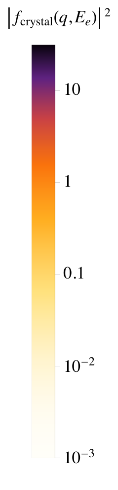
Much of the behavior of the scattering rates can be understood from the behavior of the crystal form factor, , in Eq. (21). We show the crystal form factor in Fig. 5 as a function of and , for both silicon and germanium. The rapid fall-off as increases is clearly visible. The solid line in the figure corresponds to from Eq. (16) as . The region below this line is kinematically inaccessible for any DM mass. The dashed line uses the velocity of a typical DM particle in the halo, i.e. km/s. We see that larger recoil energies require larger , for which the crystal form factor is suppressed. The implication of this is that the DM-electron scattering rates increase dramatically for smaller recoil energies, resulting in a dramatic increase in sensitivity as detector thresholds are lowered.
6.2 Cross-section reach versus detector threshold
In Fig. 6, we show the sensitivity to the DM–electron scattering cross section, , versus the DM mass, , for hypothetical silicon- and germanium-based experiments with a 1 kg-year exposure and zero background, and with various detector thresholds. The curves show 95% C.L. limits, i.e. 3.6 signal events. The blue, green, and red lines show ionization thresholds, , of 1, 5, and 10 detected electron-hole pairs, respectively, which correspond to deposited energies, , of 0.67, 12.3, and 26.8 eV in germanium, and 1.1, 15.5, and 33.5 eV in silicon (to get the corresponding ionization energy thresholds, subtract 0.67 eV for germanium and 1.1 eV for silicon from these numbers, see Eq. (26)). The three plots show results for different DM form factors, corresponding to different classes of DM models: (top left), (top right), and (bottom), see §2 for details.
As expected, the reach dramatically improves when the threshold is lowered, since the crystal form factor strongly suppresses the rate for high electron recoil energies. This improvement is most pronounced for , since lower tends to correspond to lower recoil energies. With a single-electron threshold, the difference in sensitivity for silicon and germanium targets can be accounted for by the fact that germanium is 2.6 times heavier, and so has correspondingly fewer valence electrons per kg. However, germanium targets are sensitive to slightly lower DM masses due to their lower band-gap. In addition, germanium targets become comparably more sensitive than silicon targets for ionization thresholds of due to the additional contribution from the 3d-shell electrons (see below).
Fig. 7 shows the spectrum of events as a function of the ionization signal , for different DM form-factors and masses, in silicon (left) and germanium (right) targets. The fast fall-off with shows the large gain to be made from lowering experimental thresholds towards a 1- or 2-electron threshold, especially for the steeper DM form-factors and for lower DM masses. The shape of the spectra may be useful in discriminating a signal from background.
In germanium, the 3d-shell electrons dominate the rate for eV, corresponding to electron-hole pairs (the 3d-shell electrons lie about 15 eV below the bottom of the valence band and 24 eV below the bottom of the conduction band). The intuitive reason for the 3d-shell electrons dominating over the valence electrons at large can be seen from Eqs. (9) and (10). The typical velocity of the 3d-shell electrons, and hence the typical momentum transferred from the DM, is larger than for the valence electrons, so that the 3d-shell electrons can dominate if they are kinematically accessible.66 6 For even larger deposited energies, eV, it is likely that the deeper shells will dominate the rate, for both silicon and germanium. We show the effect of neglecting the 3d-shell electrons in Fig. 15 in Appendix D, where we compare the cross-section reach and the recoil spectrum generated by DM scattering with and without the inclusion of the 3d-shell electrons. The effect is significant for ionization thresholds above or 8, but not important at lower thresholds.
We note that there are some differences between our results and those in [25, 9]. In [9], only the case was considered and we find that the new computation predicts a somewhat lower rate. We find that the shape of the recoil spectra in [25] is noticeably different from ours, which gives rise to several differences in the expected limits for the different thresholds. Furthermore, for germanium, we also include the 3d-shell electrons, which can be important as discussed above.
6.3 Comparison with existing XENON10 limit and discussion of background
We see from Fig. 6 that to surpass the existing limits obtained with XENON10 data [31], a germanium- or silicon-based experiment with an ionization threshold of 10 electrons would require a background-free exposure of less than 1 kg-year. However, with a single-electron threshold, such an experiment would surpass the XENON10 limit at all masses with a background-free exposure of around 1 kg-day for , 10 g-days for , or just a 1 g-day for . In addition, with any exposure such an experiment would place the first ever bounds in the 1-5 MeV mass range, below the threshold of the XENON10 search. The XENON10 detector had a threshold of one electron with an detection efficiency, but to obtain one electron required an energy of at least 12.4 eV to overcome the binding energy of an electron in the outer shell.77 7 Note that in [31], the electrons were treated as bounded inside free (xenon) atoms, unlike the electrons in the semiconductor targets here. Moreover, the background in the XENON10 data was much larger than conventional nuclear-recoil background, so that the number of DM events leading to single (two, and three) electrons was only limited, at 90% C.L., to be less than 8,550 (1,550, and 330) counts/kg/year, respectively.
While the single-electron background in the XENON10 data was rather large, its origin is likely specific to its dual-phase detector setup. Many of the single electron backgrounds likely had one, or a combination, of the following origins [31]: (i) electrons, trapped in the potential barrier at the liquid-gas interface, were randomly drawn into the gas phase (these transiently trapped electrons likely originated from other background events that caused xenon atoms to ionize); (ii) photo-dissociation of a negatively charged -ion, which received its negative charge from a drifting electron that originated from another event; (iii) field emission from the cathode. XENON100 and LUX may face similar challenges, although an analysis is still in progress.
The semi-conductor targets will not suffer from these same detector-specific backgrounds. They will, of course, have their own unique experimental challenges to deal with, including detector noise and dark current, as we will discuss in more detail in §6.5 for DAMIC and SuperCDMS. These will likely be the limiting instrumental factors in setting the threshold for a particular experiment. Once these challenges are overcome, one needs to deal with the physics backgrounds. As argued in [9], neutrinos are not an important source of background even for the largest exposures considered in this paper ((20 kg-years) for SuperCDMS, see §6.5). Compton scattering or other events that produce recoiling electrons will usually lead to a much larger energy deposition and most of them could thus be vetoed, although some backgrounds will persist to the lowest energies. The size of this background will depend on the shielding and purity of the materials around the detector; for SuperCDMS at SNOLAB, the Compton background is estimated to be events/kg/day/keV [104]. Assuming that it is flat at low energies, this translates into events/eV for 20 kg-years, which would be negligible. We do not expect there to be backgrounds from neutrons, and (cosmogenic) x-ray lines will lie well above our energies of interest. Surface events and other, unknown, backgrounds may be present at low energies. As experiments reach the required sensitivity to probe the few-electron events expected from LDM scattering off electrons, a better understanding of all backgrounds will emerge allowing for an attempt to mitigate them if necessary. It is possible that a spectral analysis of a signal will further allow for the removal of some background events. Our assumption of zero background for the plots should be taken as the best-case scenario.
6.4 Annual Modulation
Even with a significant background event rate, it may be possible to distinguish a signal from background using annual modulation, as long as the background is stable on year time-scales. Annual modulation is a distinguishing feature of a LDM scattering signal [105, 9], occurring due to the change in the earth’s velocity through the DM halo as it rotates around the Sun. For a standard smooth and isotropic DM velocity distribution, the modulation is approximately sinusoidal with year period and a peak around June 2nd (the presence of DM streams or non-trivial DM structure may complicate this, as may gravitational focusing by the Sun [106, 68], which we do not include). The modulation fraction, , is defined to be the ratio of the amplitude of the modulating signal to the median signal rate, which for our assumed halo profile (see Appendix B) corresponds to
| (30) |
where represents the rate at time of year .
For DM scattering off electrons, the modulation fraction can be significantly larger than for the usual elastic scattering of (heavy) WIMPs off nuclei. As we saw in Fig. 5 (see discussion in §3.1), DM–electron scattering relies on the tail of the DM velocity distribution, especially for energies above 5 –10 eV. We plot the modulation fraction in Fig. 8. The left and center plots show as a function of ionization for different masses and DM form-factors for the two elements. rises from a few percent for single-electron events to above 10% for events with more than 3 electrons. Comparing with the spectrum in Fig. 7, we see that there is a trade-off between modulation fraction and event rate. Events with several electron-hole pairs provide large modulation without sacrificing too much in the rate, and may give the best prospects for annual modulation searches depending on the background. The modulation fraction also rises near the mass threshold, as we show on the right of Fig. 8 for ionization thresholds of and 5. Note that the high-mass value of for the single-electron threshold, at 4 –6%, is larger than the values in the bin of the left and center plots, because the total rate is not dominated by the single-electron events.
Once a signal is found in an electron scattering search, increasing the exposure of the experiment until the annual modulation can be tested will be a crucial step in claiming a DM discovery. In Fig. 9 we show the discovery reach of an annual modulation search in the mass–cross-section plane. We calculate this cross section by requiring
| (31) |
where is the modulation amplitude, is the total number of signal events, and is the number of background events. The thick curves in Fig. 9 show the discovery reach for different thresholds and DM form-factors, assuming a background-free exposure of 1 kg-year. (A non-zero background will of course weaken the reach, following the equation above.) This figure mirrors Fig. 6, which shows the exclusion reach obtained using a simple counting search instead of a modulation search, but otherwise with the same assumptions. The curves of Fig. 6 are replotted as the thin curves in Fig. 9, for comparison. We see that a substantial discovery reach is possible with a 1 kg-year exposure: at low masses for , and at all masses for or .
Finally, we comment that taking into account the directional (sub-daily) modulation, which is expected in crystalline detectors, will further allow for an improved sensitivity to a DM signal. As discussed in §3.2.2, we have averaged-out such directional effects in this work, and we postpone their study to future work.
6.5 Prospects for near-term experiment
In this subsection, we discuss the near-term prospects for electron-scattering searches with the DAMIC and SuperCDMS experiments.
6.5.1 DAMIC
DAMIC [107, 108, 109] uses thick, fully-depleted silicon CCDs for their target material. These CCDs are ten times more massive than conventional CCDs, allowing them to be competitive targets for DM direct detection. In [108], DAMIC used one 0.5 g CCD to perform an engineering run, obtaining an exposure of 107 g-days. They were able to constrain DM-nuclear scattering for DM masses almost as low as 1 GeV. Work is ongoing to increase the total mass of the detector (by using more CCDs) as well as the detector’s sensitivity to low threshold energies (by using so-called “Skipper CCDs”) [67].
The first direct detection limit using a semi-conductor target.
Here we investigate the (albeit weak) constraints on DM-electron scattering from their existing result, and give reach estimates based on their projected detector improvements. For the engineering run [108], DAMIC used a single 0.5 g CCD, for an exposure of 107 g-days. They obtained the following values for the read-out noise and the dark current:
- (i)
A readout noise of below 2 electrons/pixel, corresponding to eV = 7.2 eV of r.m.s. readout noise. The CCD has about 4.2 million pixels, so that one requires a threshold of electrons ( eV) for the noise to produce a signal above threshold in less than one pixel. DAMIC chose a threshold of eV ( electrons) for the search for DM-nuclear scattering; we expect pixels to reach this threshold. In our recast of their data for DM-electron scattering below, we will use the same 40 eV threshold.
- (ii)
A dark current of electron/CCD/day (at the chosen 120 K operating temperature). Since the exposure of the CCD is a few hours, before being read-out within a few minutes, the threshold is limited by the read-out noise, and not the dark current.
We can use the result in [108] to constrain DM-electron scattering. We will assume that the efficiency to select electron recoil events is the same as selecting nuclear recoils, i.e. . Fig. 12 in [108] shows the data that was recorded by DAMIC, and we see that zero events were recorded in the first bin above the threshold (40 eV to 100 eV). This may be as a result of the efficiency being very low in this bin; nevertheless, it could also be a sign that backgrounds may be small at such low energies, boding well for future runs with even lower energy thresholds. In any case, this information is sufficient to derive the current DAMIC limit on LDM, which we show with a green shaded region (bounded by a green line) in Fig. 1. We see that with the current threshold, the form-factor suppression is too large for this constraint to compete with the existing XENON10-based limit [31]. Nevertheless, this is the first direct detection limit for sub-GeV DM using a semi-conductor target.
Projections for future DAMIC runs with improved “Skipper” CCDs.
There are two main challenges that need to be overcome by DAMIC (and similar experiments) to allow them to push to low thresholds [67]: (i) reduce the noise in reading out the ionization deposited in the detector, and (ii) reduce the dark current. The read-out noise can be reduced substantially by taking more time to read the CCD, while the dark current (i.e. genuine electron-hole pairs produced by thermal excitations in the silicon substrate) can be reduced by lowering the temperature and improving the quality of the silicon. The contribution from the dark current will increase with the readout time, so it will take some optimization to find a way to reduce the readout noise while keeping the contribution from the dark current manageable. Lowering the temperature also reduces the electron mobility in the substrate, requiring a careful trade-off. Here we project what future data runs can achieve with the improved DAMIC Skipper CCDs.
The DAMIC Collaboration has been working on so-called “Skipper CCDs”, which will reduce the r.m.s. read-out noise down to 0.2 electrons/pixel/day, with the possibility of going down to 0.1 electrons/pixel/day [108, 67]. This is done with a new output circuit that enables multiple read-outs. The size of the CCDs can be anything up to million pixels (Mpix) [110], but we will assume 8 Mpix for the projections below. The 0.2 (0.1) electrons/pixel/day correspond to read-out noise of 0.72 (0.36) eV; assuming gaussian noise, the 0.1 electron/pixel/day will allow for sensitivity down to single electrons, although the 0.2 electrons/pixel/day may require a threshold of two electrons to avoid the noise faking a DM signal. However, for such low read-out noise, the dark current becomes the limiting factor in determining the energy threshold. Significant non-gaussian tails could change this conclusion.
The dark current has been measured currently at electrons/pixel/day [110]. As mentioned above, lowering the operating temperature and improving the silicon substrate quality will decrease this, and it is reasonable to expect further improvement; the theoretical lower limit is [110]. Below we provide projections under both assumptions.
| Ionization threshold | dark current: elec./pixel/day | dark current: elec./pixel/day | ||
|---|---|---|---|---|
| 1 kg-day | 100 g-year | 1 kg-day | 100 g-year | |
| 320.0 | ||||
| (, ) | ||||
| 0.1 () | 4.2 () | |||
The effect of the dark current on the threshold depends on the number of pixels and the exposure length of the CCD. The CCD is read pixel-by-pixel, and can be read continuously from one side to the other, before cycling back again to the beginning. We will assume that the 8 million pixels of the CCD are all read in one hour, so that its exposure is one hour for the purposes of calculating the dark current. We will consider the following two scenarios for the number of CCDs, the mass, and exposure (we assume an efficiency of 1 for making our projections below):
- (i)
There are currently four prototype skipper CCDs, each with a mass of 2.5 g, which were produced as part of an R&D project (these will be deployed at the MINOS near site this year). For our first set of projections, we will assume that data is taken over 100 days (livetime), for a total exposure of 1kg-day.
- (ii)
If the testing of the skipper CCDs at MINOS goes well, one can expect that several more of them will be deployed to search for DM. Thus, for our second set of projections, we will assume that 40 CCDs are deployed (for a total mass of 100 g) and that data is taken again over 365 days (livetime) for a total exposure of 100 g-years.
Table 1 gives the expected number of events with at least electron-hole pairs for the two scenarios assuming Poisson statistics. We see that DAMIC could have a threshold of 2 electrons if the dark current can be reduced to below electrons/pixel/day, but a 3-electron threshold is required for the present dark current rate of electrons/pixel/day. In Fig. 1, we show solid green lines that indicate the 95% C.L. prospects for the entries marked with a star (), i.e. we show the cross section to obtain 3.6 signal events, assuming zero background events. We also show the reach of an annual modulation search for the entry marked with a dagger (), i.e. a 2-electron threshold with no background in a 100 g-year exposure. This is shown by the dashed green line in Fig. 1. We checked that the prospects from annual modulation for the entry marked with diamond () are very similar. We see from these projections that DAMIC can significantly improve upon the current XENON10 limit, especially at the lowest DM masses.
6.5.2 (Super)CDMS
The CDMS experiment uses cryogenic solid state detectors operated at temperatures below mK. In the WIMP search, they distinguish electron from nuclear recoils by measuring the ratio of the ionization versus phonon energy deposited into the crystal. This ratio will be smaller for nuclear recoils than for electron recoils. Here, we are interested in their ability to detect electron recoils.
The signal from a low-energy recoiling electron can be dramatically enhanced by applying a relatively large bias voltage, , across the target material. The work done in drifting an electron-hole pair out of the crystal, , is emitted as Luke-Neganov [111, 112, 113] phonons, which will be picked up by the phonon sensors. This was done for “CDMSlite”, which has yielded electron recoil thresholds with an (1) detection efficiency of 170 eV (i.e. electrons) [89]. Here we discuss the prospects of future versions of SuperCDMS.
In Fig. 1, we show 3 projections for SuperCDMS, two for silicon (with an exposure 10 kg-years) assuming an electron-hole pair threshold, , of either 4 or 1, and a signal detection efficiency of 0.7, and one for an annual modulation search assuming with the same exposure and efficiency. The cross-section reach for germanium is very similar to those of silicon.
The electron-hole-pair thresholds are based on the following assumptions. The threshold is based on the numbers used by SuperCDMS for Snowmass [63], while the threshold is based on an ambitious but achievable best-case scenario. For Snowmass, a phonon energy resolution of 50 eV was assumed. As there may be non-gaussian tails, a threshold was assumed, corresponding to a threshold of eV. Taking the bias voltage to be 100 V, this translates into , which we round up to 4. For the second set of projections, we assume that further R&D can push the noise threshold down to better than 14 eV, which is ambitious but achievable in principle [114]. A threshold corresponds to 100 eV, so that a bias voltage of 100 V is sufficient to achieve sensitivity to . In practice, the bias voltage can be optimized as well. A larger bias voltage would allow for a reduced threshold in terms of the number of electron-hole pairs needed to pass the phonon energy threshold, but could lead to breakdowns of the substrate. However, it has been demonstrated that the bias voltages needed for sensitivity to are achievable in both silicon and germanium [66].
As can be seen from Fig. 1, SuperCDMS has the potential to improve drastically upon the existing XENON10 limit, especially at low DM masses.
7 Conclusions
Direct detection experiments have so far primarily focused on searching for WIMPs, and as a result of an intense research effort, the path forward in this direction is rather well-defined. Within the next decade, WIMPs will either be found or become significantly less motivated. However, other theoretically motivated candidates exist that could constitute the DM in our Universe. In this work, we focused on a class of DM candidates that have a mass between a few-hundred keV to a GeV. We showed that tremendous progress can be made in exploring the direct-detection parameter space of these candidates over the next few years, by searching for DM-induced electron recoils in experiments with targets that consist of semiconductor materials. The technology currently used in WIMP searches can be adapted for such light-DM searches by improving the ionization sensitivity, and this is being actively pursued. The backgrounds are expected to be quite different in nature to those in WIMP searches, and there is reason to believe that they will be small and controllable.
The calculation of the DM-electron scattering rate and the subsequent electron recoil spectrum in semiconductor targets is much more challenging than for DM-nuclei scattering. We have provided detailed formulae for the scattering rate and recoil spectrum, expressed in terms of simple DM properties and a target-dependent “crystal form factor”, which encodes the quantum structure of the target electrons. We numerically calculated the crystal form factor for germanium and silicon with our code QEdark, which is based on the software package Quantum Espresso that calculates the crystal wave functions and energy levels. Convergence tests indicate that our results are accurate at the few percent level. QEdark will be publicly available at ddldm.physics.sunysb.edu, together with the crystal form factors. With these, upcoming experiments can derive their own sensitivities or limits.
The crystal form factor is a steeply falling function of the electron recoil energy. Consequently, even a small improvement in an experiment’s detector threshold translates into a significant increase in the sensitivity to DM-electron scattering. We have provided the projected sensitivity for a variety of experimental thresholds, showing that upcoming experiments including DAMIC and SuperCDMS can probe orders of magnitude of unexplored DM parameter space in the next few years. In addition to setting limits, sub-GeV dark matter can be discovered via its expected modulation signal. We showed that in the case of electron-scattering, annual modulation is sizable and could provide the necessary signal for discovery. Additional sub-daily modulation is expected due to the orientation-dependent nature of scattering in crystalline detectors. We have ignored directionality in this work, deferring it to future study.
Calculating the experimentally observable signal requires a conversion from energy deposition to the ultimate ionization signal. This conversion requires a detailed knowledge of the secondary scattering processes in crystals, at energies below the existing experimental sensitivity. We therefore used a phenomenological model for secondary interactions, and studied its possible systematic uncertainties using a Monte Carlo model. We find that our predictions suffer from systematic uncertainties of order a few tens of percent, and is likely conservative. Further theoretical and experimental study of secondary interactions would be useful to improve the modeling of this conversion.
To summarize, our work provides the necessary tools for experiments which use semiconductor targets to search for sub-GeV dark matter to derive accurate limits. Technologies adapted from WIMP searches and currently under development can be employed in searches for sub-GeV dark matter. This highly-motivated direction in dark matter searches is a natural progression from the WIMP program, and we expect that it will take a leading role in the search for dark matter.
Note added:
While this work was being completed, Ref. [68] appeared, which also deals with DM-electron scattering in germanium. Ref. [68] is complementary to our work, its main point being the effect of “gravitational focusing” on the modulation signal of DM-electron scattering. Ref. Lee:2015qvar derives scattering rates using a semi-analytic approach, which builds on the method of Ref. [25], but is significantly less detailed than the method we have presented here. We find that their results are comparable to ours within a factor of a few, but with some notable differences. In particular, Ref. [68] finds increasingly higher rates than us at increasingly higher recoil energies. Most strikingly, Ref. [68] finds that scattering of the 3d shell electrons dominates the total rate when it is kinematically accessible (we find the the 3d shells cause a bump in the spectrum, but with a rate subdominant to lower energy events). We attribute these differences to the inherent sensitivity of the calculation to the tails of the electron wavefunctions for energies above (10 eV), as we discussed in §3.1.
Acknowledgments
We are very grateful to Julien Billard, Enectali Figueroa-Feliciano, Matt Pyle, and Javier Tiffenberg for extensive discussions and correspondence on the experimental capabilities of SuperCDMS and DAMIC. We also thank Philip Allen, Brian Batell, Juan Estrada, Eder Izaguirre, Gordan Krnjaic, Samuel Lee, Mariangela Lisanti, Deyu Lu, Aaron Manalaysay, Siddharth Mishra-Sharma, and Benjamin Safdi for many useful discussions. R.E. is supported by the DoE Early Career research program DESC0008061 and through a Sloan Foundation Research Fellowship. T.-T.Y. is supported also by grant DESC0008061. M. F.-S. and A.S. acknowledge support from DoE grant DE-FG02-09ER16052. J.M. is supported by grant DE-SC0012012. T.V. is supported in part by a grant from the Israel Science Foundation, the US-Israel Binational Science Foundation, the EU-FP7 Marie Curie, CIG fellowship and by the I-CORE Program of the Planning and Budgeting Committee, and The Israel Science Foundation (grant NO 1937/12). J.M. and T.-T.Y. wish to thank the hospitality of the Aspen Center for Physics, which is supported by National Science Foundation grant PHY-1066293, where this work was completed. This research used resources of the National Energy Research Scientific Computing Center, a DOE Office of Science User Facility supported by the Office of Science of the U.S. Department of Energy under Contract No. DE-AC02-05CH11231 and the HANDY computer cluster at the Stony Brook University Institute for Advanced Computational Science.
Appendix A Derivation of scattering rate formulae
A.1 General formula for dark matter-induced electronic transitions
If a DM particle scatters with an electron in a stationary bound state such as in an atom, it can excite the electron from an initial energy level 1 to an excited energy level 2, by transferring to it energy and momentum . The cross section for this process can be derived in a standard way using non-relativistic quantum mechanics, but here we derive it starting from the usual formula for the cross-section in field-theory, in order to make easier connection with the underlying particle physics. We treat the electron as being bound in a static background potential – in other words we approximate the atoms as being infinitely heavy objects which can absorb momentum without recoiling. This is an excellent approximation ( error), since the momentum-transfers we will be interested are typically of order keV.
The cross section for free 2 2 scattering is given by
| (32) |
where is the usual field-theory matrix element, and represents its absolute square averaged over initial spins and summed over final spins.
If the electron were unbound, the non-relativistic scattering amplitude would be given by
| (33) |
where is plane-wave state for a DM particle of momentum and an electron of momentum , is the interaction Hamiltonian, and is an unimportant coefficient. However, because the electron is bound it is instead given by
| (34) |
where , are the (unit normalized) momentum-space wavefunctions of the initial and final electron levels. We have purposefully used plane-wave normalization for both the free and bound electron states: , where is the volume of space (which always cancels in the end).
To find the cross section for this excitation process, we can use the free 2 2 scattering cross section formula but with two replacements: one to account for the modified scattering amplitude, and the other to account for the different final-state phase space. Squaring Eqs. (33, 34), we see that the bound-state scattering amplitude is accounted for by making the replacement
| (35) |
where is the atomic form factor,
| (36) |
Fourier transforming Eq. (36) gives the definition given in Eq. (14).
Since there is only one final electron state being considered, we also need to remove the usual final-state phase space integral:
| (37) |
Combining Eqs. (32, 35, 37), we can write the formula for the cross-section for a DM particle to excite an electron from level 1 to level 2:
| (38) |
Since we are in the non-relativistic regime, the energies are given by
| (39) | ||||
| (40) |
Using the following definitions [9] to parametrize the underlying DM–electron coupling
| (41) | |||
| (42) |
the cross section simplifies to
| (43) |
A.2 Average rate in a dark matter halo
The actual rate of excitation events, for a given transition and a given target electron, is found by multiplying Eq. (43) by the DM density and averaging over the DM velocity distribution ,
| (44) |
In general, both the electron wavefunctions and the DM velocity distribution will not be spherically symmetric. As noted in [9], the rate will then depend on the orientation of the target with respect to the galaxy. Here we ignore this interesting complication, and approximate the velocity distribution as being spherically symmetric. We can then use the integral to eliminate the -function in Eq. (43), giving
| (45) |
Here has its usual definition,
| (46) |
and is a function of and the energy transfer given by
| (47) |
A.3 Ionizing an isolated atom
For the purposes of connecting with previous work [9], in this subsection we consider ionization of electrons bound in isolated atomic potentials. We derive the ionization rate of such a system, assuming a spherical atomic potential and filled shells. This approximation was used in [9] to model a liquid xenon target material, and the results below reproduce Eqs. (5) and (6) of that paper. The full calculation of event rates in liquid xenon would require knowledge of electron wavefunctions in the dense, disordered xenon liquid. This is a more challenging calculation than for a semiconductor crystal, but can in principle be performed with similar methods – we leave this for future work. The corrections, however, can be argued to be small, lowering the ionization threshold and increasing the event rate.
An electron ionized from an atom can be treated as being in one of a continuum of positive-energy bound states. These states are affected by the potential well of the atom, but can be approximated as free particle states at asymptotically large radii. We denote their wavefunctions as , where and are angular quantum numbers, and is the momentum at asymptotically large radius. The energy of such a state is therefore .
The ionization rate for such an atom is found by taking Eq. (45), summing over occupied electron shells, and integrating over the phase space of all possible ionized states. Since these are asymptotically free spherical-wave states, the phase space is
| (48) |
when the wavefunction normalization is, as in [9], taken to be
| (49) |
Plugging this in, the ionization rate is given by
| (50) | |||||
where is the binding energy of occupied state .
Since the potential is assumed to be spherically symmetric, and we are ionizing a full atomic shell, we can sum over initial and final angular momentum variables and the result cannot depend on the direction of . This means we can define the dimensionless ionization form factor,
| (51) |
After applying this definition to the previous equation, we can replace the integral with , giving
| (52) |
This reproduces the formulae given in [9].
A.4 Excitations in a semiconductor crystal
In the periodic lattice of a semiconductor crystal, the electron energy levels form a complicated band structure, with an energy gap separating the filled valence bands and the unoccupied conduction bands (Fig. 4). Each possible electron level is labelled by a band index and a wavevector in the first Brillouin Zone (BZ). Due to the periodicity of the potential, the wavefunctions of these states are in Bloch form,
| (53) |
where the ’s are the reciprocal lattice vectors. Here is the volume of the crystal, and the wavefunctions are taken to be unit-normalized, so that
| (54) |
(We use the relations and .)
With this form for the wavefunctions, the form factor Eq. (14) to excite from valence level to conduction level becomes
| (55) | ||||
| (56) |
We define the term in the absolute square in Eq. (56) to be :
| (57) |
Inserting this into Eq. (45), we can use the -function to eliminate the integral, giving
| (58) |
The total excitation rate for an electron in level is found by summing Eq. (58) over all unfilled final energy levels ,
| (59) |
Note that we do not sum over final electron spins here as that sum has already been included in the definition of .
The total rate of excitation events in the crystal, , is given by summing Eq. (59) over all filled initial levels ,
| (60) |
Here the extra factor of 2 is the sum over the two degenerate spin states of the filled valence bands.
Putting this together gives the total excitation rate in a crystal,
| (61) |
where again . Note that this is the total event rate for the whole crystal, and so it is appropriate that it is proportional to the volume of the whole crystal. Since the dependence on the DM velocity distribution and interaction type are entirely encoded in and , which are functions only of the momentum transfer and energy deposited , it is useful to insert delta-functions into the above expression as follows:
| (62) |
Appendix B Derivation of inverse mean speed,
In this section, we will derive analytic expressions for . For simplicity we assume that the DM velocity distribution, , takes the form of a Maxwell-Boltzmann distribution in the galactic rest frame, with a hard cutoff at the galactic escape velocity. In the Earth’s frame the velocity distribution then takes the form
| (65) |
where is the DM velocity in the Earth frame, and is the Earth’s velocity in the galactic rest frame. We take km/s for the typical velocity, and km/s for the escape velocity. We take km/s for the average Earth velocity relative to the DM halo, adding (subtracting) 15 km/s for the Earth velocity in June (December).
The normalization factor is determined by requiring , giving
| (66) |
Using these values, we obtain [cm/s]3 or in natural units.
We then define the function ,
| (67) |
where is the angle between the velocity and the velocity of the Earth. We can explicitly solve Eq. (67), but need to consider two cases:
- 1.
- 2.
where
This gives us
| (68) | |||||
where the subscript corresponds to the case number. Note that the two cases converge to the same value for .
Appendix C Convergence of the Numerical Results
In this section, we investigate the dependence of our calculation on the kinetic-energy cutoff, , (see Eq. (24)) and on the -point mesh. The choice of determines the maximum allowed three-momentum transfer , which impacts the maximum that we sample. Truncating the range of can have more of an effect for high DM masses and high electron thresholds, since these two regimes depend on high values of . On the other hand, the -points included in the mesh determine the computationally allowed values of . A higher-resolution mesh is particularly important for low transitions to the bottom of the conduction band, and is therefore especially important for low DM masses and low electron thresholds.
In Fig. 10, we show the dependence of in Eq. (16) on for different and . The choice of (top axis) determines the range of (bottom axis). In Fig. 11, we show the ratio of the rate for different values of to the rate at Ry for GeV for silicon targets. We see that the error in the rate with our choice of Ry is . The convergence in germanium is slightly worse due to the fact that we are solving for the 3d electrons instead of including them in the pseudopotential. This effect is greatest near the 3d shell energies (a few percent uncertainty), as seen in Fig. 12. In left plots of both Fig. 11 and 12, we see a step-like transition between 30 Ry and the other curves for 11e because 30 Ry is not a high enough energy cutoff to accurately calculate the rate for 11e. The irregular behavior in the distributions on the right side of Fig. 12 are from the semicore electrons in Ge. We do not see the same behavior in Fig. 11, which considers Si and no semicore electrons.
We investigate the effects of our choice of -point mesh on our results in two ways.88 8 We do this only for the valence electrons without including the 3d-shell electrons, since energy of the latter are nearly constant as a function of . In any case, the 3d-shell electrons are important at large , while the choice of -point mesh is important only at low . First, we vary the number of -points in our mesh and find that there is sensitivity to our choice at low masses and thresholds, see Fig. 13. Second, we perturb each point on the mesh with a random shake of amplitude up to half the lattice-spacing so as to cover the entire -space. We use an energy cutoff of Ry and 243 -points. The amplitude of our perturbations is a.u. as the lattice spacing for 243 -points is 0.17 a.u. We run 10 independent simulations and plot the results in Fig. 14. We find that our choice of -point mesh does not appreciably affect our results for masses above MeV.
Appendix D The importance of the 3d-shell in germanium
The importance of the 3d-shell electrons in germanium are illustrated in Fig. 15. We see that they dominate the rate at high recoil energies and thus for high thresholds. We discuss this in more detail in §6.2.
Appendix E A Monte Carlo model of secondary scattering
In the main results of this paper, we modeled the ionization response of a target crystal with the linear treatment described in §5. For comparison, here we attempt to mock-up the secondary scattering with a Monte Carlo model, following [101]. The deposited energy is randomly split between an initial electron and hole. In each following step, each electron or hole with energy above a threshold then generates an extra electron-hole pair, with the energy being randomly split between the three particles. This is iterated until all particles have energy less than .
The random energy splittings follows a distribution that weights all phase space volume equally, with the density of states assumed to grow as above and below the bandgap, as in a simple 2-band free electron/hole system. Explicitly, for the initial splitting the probability distribution for energy to split into energies and has the form
while for the subsequent splittings it has the form
where electon/hole energies are measured above/below the upper/lower edge of the band gap. We ignore phonon losses during the cascade – these are understood to be quantitatively fairly small, and should not affect the qualitative conclusions.
The output of the Monte Carlo model is a probability distribution to get ionization given a deposited energy . Given the band-gap energy of eV (1.11 eV) in germanium (silicon), we find that eV (3.1 eV) reproduces the measured values of for high energy recoils (see Eq. (27)). The distributions for both elements have Fano factors of for all energies above eV, consistent with measurements. We illustrate the probability distributions in Fig. 16. In Fig. 17, we show the effect on the event rate of using this model rather than the naive linear model of §5. For thresholds of 2 to 4 electron-hole pairs, downward fluctuations reduce the rate compared to the naive estimate. For higher thresholds, occasional upward fluctuations combined with the steeply falling recoil spectrum lead to an increase in the rate. However, the two models are consistent within a few tens of percent.
Appendix F Review of Density Functional Theory and Pseudopotentials
In this appendix, we review the formalism of density functional theory (DFT), explain in more detail the approximations used in the computation of the wavefunctions, and further explain the numerical methods.
F.1 Electronic structure within DFT
Non-relativistic electrons interacting electrostatically with fixed nuclei are described by the electronic structure Schrödinger equation
| (70) |
where label electrons, labels nuclei, and is the atomic number of nuclei . The first term in the Hamiltonian is the electron kinetic energy , the second term is the Coulomb electron-nucleus attraction and the third term is the electron-electron Coulomb repulsion . The constant nuclei-nuclei term has been omitted. Even though the question is well-posed, obtaining the many-electron wavefunctions computationally is an extremely difficult task because of the exponential scaling of the problem with the number of electrons . This method becomes then helpless for applications of interest, so in practice one needs to resort to approximate methods.
DFT is a reformulation of the interacting quantum many-body problem in terms of functionals of the particle density . For the case of electrons, the Hohenberg-Kohn theorems [91] imply that all properties of the interacting system are determined once the ground state electron density is known. Minimizing an energy functional will provide the ground state density and the ground state energy . Unfortunately this energy functional is not known in general. The Kohn-Sham method [92] overcomes this obstacle by replacing the description strictly in terms of functionals for a wavefunction formulation: the system of interacting electrons with Hamiltonian is mapped into a system of independent electrons under the presence of an auxiliary potential which produces the same ground state density as . This is of great advantage because, once this mapping is built, one has to solve the much simpler independent-particle system in order to obtain and . However, this comes at the expense of having to use an approximate auxiliary potential . Typically, is split into the mean-field Hartree potential and the so-called exchange-correlation potential , where the approximations are imposed. Once an approximation for has been chosen, the non-interacting electron Schrödinger equation
| (71) |
which are known as the Kohn-Sham equations, are solved to get the auxiliary Kohn-Sham wavefunctions . From these, the density can be obtained as , where are the occupation numbers ( for spin-unpolarized systems) as well as the ground state energy by evaluating the energy density functional99 9 The connection between an energy functional and its corresponding local potential is . ,1010 10 The kinetic energy is calculated from the Kohn-Sham wavefunctions as . as well as a set of wavefunctions and eigenenergies . This problem is solved self-consistently until convergence is reached.
Expanding the wavefunctions in a finite plane-wave basis with elements labeled by the vectors and , the Kohn-Sham equations become the matrix equations
| (72) |
where the Hamiltonian is
| (73) |
It should be noted that, since the potential is local, its reciprocal space form does not depend on . Furthermore, the Kohn-Sham equations in reciprocal space Eq. (72) decouple different ’s, so the eigenvalue problem can be carried out independently at each .
Despite all the successes of DFT, several notable shortcomings are known today. The most relevant one for us is that DFT is known to give an incorrect band gap. This is due to a discontinuity in the DFT exchange-correlation potential when electrons are added above the gap [115, 116]. There are methods based on many-body perturbation theory to improve the DFT band gap and band shapes, such as the GW method [117]. However, since the largest contribution to the scattering rate comes from the low energy excitations, we choose to follow an empirical “scissor correction” approach [95, 96]. In this approach a rigid shift is imposed on the conduction bands with respect to the valence bands in order to set the band gap to the experimental values of eV for silicon and eV for germanium [97]. It is worth noting that the semiconductor band gap features a temperature variation of around meV [94], but we are choosing the room temperature band gap values for our calculation.
F.2 Energy Density Functionals
In order to be able to use DFT, a choice for the exchange-correlation functional is required. The Local Density Approximation (LDA) [92] has been remarkably successful because of its simplicity and transferability. In this method the exchange-correlation energy functional is based only on physical considerations and is approximated locally by the energy of a homogeneous electron gas (HEG) with the following density:
| (74) |
The HEG exchange [118] and correlation [119] energy functionals are well established. There are some faults in the LDA which are known to be most dramatic where the electrons are highly localized and exchange repulsions are significant. In order to correct for that, the Generalized Gradient Approximations (GGA) introduce a dependence on the density gradient in the exchange-correlation energy density
| (75) |
In this work we choose the well-established PBE functional [93] which is known to produce a broad set of properties of materials to accuracies of order a few percent [120]. Since LDA functionals tend to underestimate the energies of excited states compared to GGA functionals, we find a difference in cross-section sensitivity of around 10-20%, with a larger difference at higher thresholds.
F.3 Pseudopotentials
The valence electrons are responsible for the formation of interatomic bonds and their wavefunctions are in general delocalized, spanning over interatomic distances. The core electron wavefunctions, however, are very localized around the nucleus and they barely change from the isolated atom to the condensed matter phase. This fact allows to use the atomic core electron wavefunctions in the condensed matter phase by replacing the bare positive nuclear Coulomb potential and the negative Coulomb potential generated by the core wavefunctions with a pseudopotential in the Kohn-Sham problem Eq. (71). The advantage is two-fold: first, the number of electrons in the problem is reduced to the number of valence electrons and second, the only wavefunctions to be calculated are valence wavefunctions which, since they are rather smooth, do not require as fine a grid to represent them as a core electron wavefunction would, thus improving the computational efficiency. In this work we use Vanderbilt-type ultrasoft pseudopotentials [94]. The pseudopotential for Si includes the 3s and 3p electrons in the valence, while in the case of germanium, we use a pseudopotential which includes the 3d, 4s and 4p electrons in the valence.
References
- (1) M. W. Goodman and E. Witten, Detectability of Certain Dark Matter Candidates, Phys.Rev. D31 (1985) 3059.
- (2) XENON100 Collaboration, E. Aprile et al., Dark Matter Results from 225 Live Days of XENON100 Data, Phys.Rev.Lett. 109 (2012) 181301, [arXiv:1207.5988].
- (3) LUX Collaboration Collaboration, D. Akerib et al., First Results from the Lux Dark Matter Experiment at the Sanford Underground Research Facility, Phys.Rev.Lett. 112 (2014), no. 9 091303, [arXiv:1310.8214].
- (4) SuperCDMS Collaboration Collaboration, R. Agnese et al., Search for Low-Mass Weakly Interacting Massive Particles with SuperCDMS, Phys.Rev.Lett. 112 (2014), no. 24 241302, [arXiv:1402.7137].
- (5) J. Preskill, M. B. Wise, and F. Wilczek, Cosmology of the Invisible Axion, Phys.Lett. B120 (1983) 127–132.
- (6) M. Dine and W. Fischler, The Not So Harmless Axion, Phys.Lett. B120 (1983) 137–141.
- (7) L. Abbott and P. Sikivie, A Cosmological Bound on the Invisible Axion, Phys.Lett. B120 (1983) 133–136.
- (8) E. W. Kolb, D. J. Chung, and A. Riotto, Wimpzillas!, [hep-ph/9810361].
- (9) R. Essig, J. Mardon, and T. Volansky, Direct Detection of Sub-GeV Dark Matter, Phys.Rev. D85 (2012) 076007, [arXiv:1108.5383].
- (10) C. Boehm and P. Fayet, Scalar dark matter candidates, Nucl.Phys. B683 (2004) 219–263, [hep-ph/0305261].
- (11) M. J. Strassler and K. M. Zurek, Echoes of a Hidden Valley at Hadron Colliders, Phys.Lett. B651 (2007) 374–379, [hep-ph/0604261].
- (12) D. Hooper and K. M. Zurek, A Natural Supersymmetric Model with MeV Dark Matter, Phys.Rev. D77 (2008) 087302, [arXiv:0801.3686].
- (13) I. Cholis, L. Goodenough, and N. Weiner, High Energy Positrons and the WMAP Haze from Exciting Dark Matter, Phys.Rev. D79 (2009) 123505, [arXiv:0802.2922].
- (14) N. Arkani-Hamed, D. P. Finkbeiner, T. R. Slatyer, and N. Weiner, A Theory of Dark Matter, Phys.Rev. D79 (2009) 015014, [arXiv:0810.0713].
- (15) M. Pospelov and A. Ritz, Astrophysical Signatures of Secluded Dark Matter, Phys. Lett. B671 (2009) 391–397.
- (16) R. Essig, J. Kaplan, P. Schuster, and N. Toro, On the Origin of Light Dark Matter Species, [arXiv:1004.0691].
- (17) D. E. Morrissey, D. Poland, and K. M. Zurek, Abelian Hidden Sectors at a GeV, JHEP 0907 (2009) 050, [arXiv:0904.2567].
- (18) J. L. Feng and J. Kumar, The Wimpless Miracle: Dark-Matter Particles without Weak-Scale Masses Or Weak Interactions, Phys.Rev.Lett. 101 (2008) 231301, [arXiv:0803.4196].
- (19) T. Cohen, D. J. Phalen, A. Pierce, and K. M. Zurek, Asymmetric Dark Matter from a GeV Hidden Sector, Phys.Rev. D82 (2010) 056001, [arXiv:1005.1655].
- (20) T. Lin, H.-B. Yu, and K. M. Zurek, On Symmetric and Asymmetric Light Dark Matter, Phys.Rev. D85 (2012) 063503, [arXiv:1111.0293].
- (21) A. Loeb and N. Weiner, Cores in Dwarf Galaxies from Dark Matter with a Yukawa Potential, Phys.Rev.Lett. 106 (2011) 171302, [arXiv:1011.6374].
- (22) S. Tulin, H.-B. Yu, and K. M. Zurek, Beyond Collisionless Dark Matter: Particle Physics Dynamics for Dark Matter Halo Structure, [arXiv:1302.3898].
- (23) J. March-Russell, J. Unwin, and S. M. West, Closing in on Asymmetric Dark Matter I: Model Independent Limits for Interactions with Quarks, JHEP 1208 (2012) 029, [arXiv:1203.4854].
- (24) X. Chu, T. Hambye, and M. H. Tytgat, The Four Basic Ways of Creating Dark Matter Through a Portal, JCAP 1205 (2012) 034, [arXiv:1112.0493].
- (25) P. W. Graham, D. E. Kaplan, S. Rajendran, and M. T. Walters, Semiconductor Probes of Light Dark Matter, Phys.Dark Univ. 1 (2012) 32–49, [arXiv:1203.2531].
- (26) M. Kaplinghat, S. Tulin, and H.-B. Yu, Direct Detection Portals for Self-Interacting Dark Matter, Phys.Rev. D89 (2014) 035009, [arXiv:1310.7945].
- (27) K. K. Boddy, J. L. Feng, M. Kaplinghat, and T. M. P. Tait, Self-Interacting Dark Matter from a Non-Abelian Hidden Sector, Phys.Rev. D89 (2014), no. 11 115017, [arXiv:1402.3629].
- (28) K. K. Boddy, J. L. Feng, M. Kaplinghat, Y. Shadmi, and T. M. P. Tait, Strongly Interacting Dark Matter: Self-Interactions and keV Lines, Phys.Rev. D90 (2014), no. 9 095016, [arXiv:1408.6532].
- (29) Y. Hochberg, E. Kuflik, T. Volansky, and J. G. Wacker, Mechanism for Thermal Relic Dark Matter of Strongly Interacting Massive Particles, Phys.Rev.Lett. 113 (2014) 171301, [arXiv:1402.5143].
- (30) Y. Hochberg, E. Kuflik, H. Murayama, T. Volansky, and J. G. Wacker, The Simplest Miracle, [arXiv:1411.3727].
- (31) R. Essig, A. Manalaysay, J. Mardon, P. Sorensen, and T. Volansky, First Direct Detection Limits on Sub-Gev Dark Matter from Xenon10, Phys.Rev.Lett. 109 (2012) 021301, [arXiv:1206.2644].
- (32) C. Bird, P. Jackson, R. V. Kowalewski, and M. Pospelov, Search for Dark Matter in Transitions with Missing Energy, Phys.Rev.Lett. 93 (2004) 201803, [hep-ph/0401195].
- (33) B. McElrath, Invisible Quarkonium Decays as a Sensitive Probe of Dark Matter, Phys.Rev. D72 (2005) 103508, [hep-ph/0506151].
- (34) P. Fayet, Constraints on Light Dark Matter and U Bosons, from Psi, Upsilon, K+, Pi0, Eta and Eta-Prime Decays, Phys.Rev. D74 (2006) 054034, [hep-ph/0607318].
- (35) C. Bird, R. V. Kowalewski, and M. Pospelov, Dark Matter Pair-Production in Transitions, Mod.Phys.Lett. A21 (2006) 457–478, [hep-ph/0601090].
- (36) CLEO Collaboration Collaboration, P. Rubin et al., Search for Invisible Decays of the Upsilon(1S) Resonance, Phys.Rev. D75 (2007) 031104, [hep-ex/0612051].
- (37) Belle Collaboration Collaboration, O. Tajima et al., Search for invisible decay of the Upsilon(1S), Phys.Rev.Lett. 98 (2007) 132001, [hep-ex/0611041].
- (38) Y. Kahn, M. Schmitt, and T. M. Tait, Enhanced rare pion decays from a model of MeV dark matter, Phys.Rev. D78 (2008) 115002, [arXiv:0712.0007].
- (39) P. Fayet, U-boson production in e+ e- annihilations, psi and Upsilon decays, and Light Dark Matter, Phys.Rev. D75 (2007) 115017, [hep-ph/0702176].
- (40) P. Fayet, Invisible Upsilon decays into Light Dark Matter, Phys.Rev. D81 (2010) 054025, [arXiv:0910.2587].
- (41) G. K. Yeghiyan, Upsilon Decays into Light Scalar Dark Matter, Phys.Rev. D80 (2009) 115019, [arXiv:0909.4919].
- (42) BaBar Collaboration Collaboration, P. del Amo Sanchez et al., Search for Production of Invisible Final States in Single-Photon Decays of (1S), Phys.Rev.Lett. 107 (2011) 021804, [arXiv:1007.4646].
- (43) A. Badin and A. A. Petrov, Searching for light Dark Matter in heavy meson decays, Phys.Rev. D82 (2010) 034005, [arXiv:1005.1277].
- (44) B. Echenard, Search for Low-Mass Dark Matter at BABAR, Mod.Phys.Lett. A27 (2012) 1230016, [arXiv:1205.3505].
- (45) N. Borodatchenkova, D. Choudhury, and M. Drees, Probing MeV Dark Matter at Low-Energy E+E- Colliders, Phys.Rev.Lett. 96 (2006) 141802, [hep-ph/0510147].
- (46) R. Essig, P. Schuster, and N. Toro, Probing Dark Forces and Light Hidden Sectors at Low-Energy E+E- Colliders, Phys.Rev. D80 (2009) 015003, [arXiv:0903.3941].
- (47) M. Reece and L.-T. Wang, Searching for the Light Dark Gauge Boson in Gev-Scale Experiments, JHEP 0907 (2009) 051, [arXiv:0904.1743].
- (48) H. K. Dreiner, S. Heinemeyer, O. Kittel, U. Langenfeld, A. M. Weber, et al., Mass Bounds on a Very Light Neutralino, Eur.Phys.J. C62 (2009) 547–572, [arXiv:0901.3485].
- (49) BaBar Collaboration Collaboration, B. Aubert et al., Search for Invisible Decays of a Light Scalar in Radiative Transitions , [arXiv:0808.0017].
- (50) R. Essig, J. A. Jaros, W. Wester, P. H. Adrian, S. Andreas, et al., Working Group Report: New Light Weakly Coupled Particles, [arXiv:1311.0029].
- (51) R. Essig, J. Mardon, M. Papucci, T. Volansky, and Y.-M. Zhong, Constraining Light Dark Matter with Low-Energy Colliders, JHEP 1311 (2013) 167, [arXiv:1309.5084].
- (52) E. Izaguirre, G. Krnjaic, P. Schuster, and N. Toro, New Electron Beam-Dump Experiments to Search for MeV to few-GeV Dark Matter, Phys.Rev. D88 (2013) 114015, [arXiv:1307.6554].
- (53) C. Boehm, M. J. Dolan, and C. McCabe, A Lower Bound on the Mass of Cold Thermal Dark Matter from Planck, JCAP 1308 (2013) 041, [arXiv:1303.6270].
- (54) K. M. Nollett and G. Steigman, BBN And The CMB Constrain Light, Electromagnetically Coupled WIMPs, Phys. Rev. D89 (2014), no. 8 083508, [arXiv:1312.5725].
- (55) BDX Collaboration Collaboration, M. Battaglieri et al., Dark matter search in a Beam-Dump eXperiment (BDX) at Jefferson Lab, [arXiv:1406.3028].
- (56) E. Izaguirre, G. Krnjaic, P. Schuster, and N. Toro, Testing GeV-Scale Dark Matter with Fixed-Target Missing Momentum Experiments, [arXiv:1411.1404].
- (57) B. Batell, R. Essig, and Z. Surujon, Strong Constraints on Sub-GeV Dark Sectors from SLAC Beam Dump E137, Phys.Rev.Lett. 113 (2014), no. 17 171802, [arXiv:1406.2698].
- (58) J. Va’vra, Molecular excitations: a new way to detect Dark matter, Phys. Lett. B736 (2014) 169–173, [arXiv:1402.0466].
- (59) E. Izaguirre, G. Krnjaic, P. Schuster, and N. Toro, Accelerating the Discovery of Light Dark Matter, [arXiv:1505.00011].
- (60) Y. Kahn, G. Krnjaic, J. Thaler, and M. Toups, DAE?ALUS and dark matter detection, Phys. Rev. D91 (2015), no. 5 055006, [arXiv:1411.1055].
- (61) Y. Hochberg, Y. Zhao, and K. M. Zurek, Superconducting Detectors for Superlight Dark Matter, Phys. Rev. Lett. 116 (2016), no. 1 011301, [arXiv:1504.07237].
- (62) J. A. Formaggio, E. Figueroa-Feliciano, and A. Anderson, Sterile Neutrinos, Coherent Scattering and Oscillometry Measurements with Low-Temperature Bolometers, Phys.Rev. D85 (2012) 013009, [arXiv:1107.3512].
- (63) P. Cushman, C. Galbiati, D. McKinsey, H. Robertson, T. Tait, et al., Working Group Report: WIMP Dark Matter Direct Detection, [arXiv:1310.8327].
- (64) XENON Collaboration Collaboration, E. Aprile et al., Design and Performance of the Xenon10 Dark Matter Experiment, Astropart.Phys. 34 (2011) 679–698, [arXiv:1001.2834].
- (65) XENON10 Collaboration Collaboration, J. Angle et al., A Search for Light Dark Matter in Xenon10 Data, Phys.Rev.Lett. 107 (2011) 051301, [arXiv:1104.3088].
- (66) E. Figueroa-Feliciano and M. Pyle private communication.
- (67) J. Estrada and J. Tiffenberg private communication.
- (68) S. K. Lee, M. Lisanti, S. Mishra-Sharma, and B. R. Safdi, Modulation Effects in Dark Matter-Electron Scattering Experiments, Phys. Rev. D92 (2015), no. 8 083517, [arXiv:1508.07361].
- (69) P. Giannozzi et al., Quantum espresso: a modular and open-source software project for quantum simulations of materials, Journal of Physics: Condensed Matter 21 (2009), no. 39 395502 (19pp).
- (70) K. Sigurdson, M. Doran, A. Kurylov, R. R. Caldwell, and M. Kamionkowski, Dark-matter electric and magnetic dipole moments, Phys. Rev. D70 (2004) 083501, [astro-ph/0406355]. [Erratum: Phys. Rev.D73,089903(2006)].
- (71) R. Essig, K. Tobioka, T. Volansky, and T.-T. Yu.
- (72) M. S. Madhavacheril, N. Sehgal, and T. R. Slatyer, Current Dark Matter Annihilation Constraints from Cmb and Low-Redshift Data, Phys.Rev. D89 (2014) 103508, [arXiv:1310.3815].
- (73) Planck Collaboration, P. Ade et al., Planck 2015 Results. Xiii. Cosmological Parameters, [arXiv:1502.01586].
- (74) R. Essig, E. Kuflik, S. D. McDermott, T. Volansky, and K. M. Zurek, Constraining Light Dark Matter with Diffuse X-Ray and Gamma-Ray Observations, JHEP 1311 (2013) 193, [arXiv:1309.4091].
- (75) SuperCDMS Collaboration, R. Agnese et al., New Results from the Search for Low-Mass Weakly Interacting Massive Particles with the CDMS Low Ionization Threshold Experiment, Phys. Rev. Lett. 116 (2016), no. 7 071301, [arXiv:1509.02448].
- (76) CRESST Collaboration, G. Angloher et al., Results on light dark matter particles with a low-threshold CRESST-II detector, Eur. Phys. J. C76 (2016), no. 1 25, [arXiv:1509.01515].
- (77) D. Curtin, R. Essig, S. Gori, and J. Shelton, Illuminating Dark Photons with High-Energy Colliders, JHEP 1502 (2015) 157, [arXiv:1412.0018].
- (78) A. Hook, E. Izaguirre, and J. G. Wacker, Model Independent Bounds on Kinetic Mixing, Adv.High Energy Phys. 2011 (2011) 859762, [arXiv:1006.0973].
- (79) M. Pospelov, Secluded U(1) Below the Weak Scale, Phys.Rev. D80 (2009) 095002, [arXiv:0811.1030].
- (80) H. Davoudiasl and W. J. Marciano, Running of the U(1) coupling in the dark sector, Phys. Rev. D92 (2015), no. 3 035008, [arXiv:1502.07383].
- (81) S. W. Randall, M. Markevitch, D. Clowe, A. H. Gonzalez, and M. Bradac, Constraints on the Self-Interaction Cross-Section of Dark Matter from Numerical Simulations of the Merging Galaxy Cluster 1E 0657-56, Astrophys.J. 679 (2008) 1173–1180, [arXiv:0704.0261].
- (82) J. Bjorken, S. Ecklund, W. Nelson, A. Abashian, C. Church, et al., Search for Neutral Metastable Penetrating Particles Produced in the SLAC Beam Dump, Phys.Rev. D38 (1988) 3375.
- (83) P. deNiverville, M. Pospelov, and A. Ritz, Observing a light dark matter beam with neutrino experiments, Phys.Rev. D84 (2011) 075020, [arXiv:1107.4580].
- (84) B. Batell, M. Pospelov, and A. Ritz, Exploring Portals to a Hidden Sector Through Fixed Targets, Phys.Rev. D80 (2009) 095024, [arXiv:0906.5614].
- (85) S. Nussinov, Technocosmology: Could a Technibaryon Excess Provide a ‘Natural’ Missing Mass Candidate?, Phys.Lett. B165 (1985) 55.
- (86) D. B. Kaplan, A Single Explanation for Both the Baryon and Dark Matter Densities, Phys.Rev.Lett. 68 (1992) 741–743.
- (87) D. E. Kaplan, M. A. Luty, and K. M. Zurek, Asymmetric Dark Matter, Phys.Rev. D79 (2009) 115016, [arXiv:0901.4117].
- (88) L. J. Hall, K. Jedamzik, J. March-Russell, and S. M. West, Freeze-In Production of Fimp Dark Matter, JHEP 1003 (2010) 080, [arXiv:0911.1120].
- (89) SuperCDMS Collaboration Collaboration, R. Agnese et al., Search for Low-Mass Weakly Interacting Massive Particles Using Voltage-Assisted Calorimetric Ionization Detection in the SuperCDMS Experiment, Phys.Rev.Lett. 112 (2014), no. 4 041302, [arXiv:1309.3259].
- (90) S. Davidson, S. Hannestad, and G. Raffelt, Updated bounds on millicharged particles, JHEP 0005 (2000) 003, [hep-ph/0001179].
- (91) P. Hohenberg and W. Kohn, Inhomogeneous Electron Gas, Phys.Rev. 136 (1964) B864–B871.
- (92) W. Kohn and L. Sham, Self-Consistent Equations Including Exchange and Correlation Effects, Phys.Rev. 140 (1965) A1133–A1138.
- (93) J. P. Perdew, K. Burke, and M. Ernzerhof, Generalized Gradient Approximation Made Simple, Phys. Rev. Lett. 77 (Oct, 1996) 3865–3868.
- (94) P. Lautenschlager, P. B. Allen, and M. Cardona, Temperature dependence of band gaps in Si and Ge, Phys. Rev. B 31 (Feb, 1985) 2163–2171.
- (95) Z. Levine and D. Allan, Linear optical response in silicon and germanium including self-energy effects, Phys. Rev. Lett. 63 (Oct, 1989) 1719–1722.
- (96) Z. Levine and D. Allan, Quasiparticle calculation of the dielectric response of silicon and germanium, Phys. Rev. B 43 (Feb, 1991) 4187–4207.
- (97) B. G. S. B. Streetman, Solid state electronic devices, Prentice Hall (2005).
- (98) C. A. Klein, Bandgap Dependence and Related Features of Radiation Ionization Energies in Semiconductors, Journal of Applied Physics 39 (Mar., 1968) 2029–2038.
- (99) B. G. Lowe, Measurements of Fano factors in silicon and germanium in the low-energy X-ray region, Nuclear Instruments and Methods in Physics Research A 399 (Feb., 1997) 354–364.
- (100) M. Lépy, J. Campbell, J. Laborie, J. Plagnard, P. Stemmler, and W. Teesdale, Experimental study of the response of semiconductor detectors to low-energy photons, Nuclear Instruments and Methods in Physics Research Section A: Accelerators, Spectrometers, Detectors and Associated Equipment 439 (2000) 239 – 246.
- (101) R. C. Alig, S. Bloom, and C. W. Struck, Scattering by ionization and phonon emission in semiconductors, Phys. Rev. B 22 (Dec., 1980) 5565–5582.
- (102) R. Catena and P. Ullio, A novel determination of the local dark matter density, JCAP 1008 (2010) 004, [arXiv:0907.0018].
- (103) P. Salucci, F. Nesti, G. Gentile, and C. Martins, The dark matter density at the Sun’s location, Astron.Astrophys. 523 (2010) A83, [arXiv:1003.3101].
- (104) E. Figueroa-Feliciano private communication.
- (105) A. Drukier, K. Freese, and D. Spergel, Detecting Cold Dark Matter Candidates, Phys.Rev. D33 (1986) 3495–3508.
- (106) S. K. Lee, M. Lisanti, A. H. G. Peter, and B. R. Safdi, Effect of Gravitational Focusing on Annual Modulation in Dark-Matter Direct-Detection Experiments, Phys.Rev.Lett. 112 (2014), no. 1 011301, [arXiv:1308.1953].
- (107) J. Estrada, Dark Matter in CCD’s (DAMIC), .
- (108) DAMIC Collaboration Collaboration, J. Barreto et al., Direct Search for Low Mass Dark Matter Particles with CCDs, Phys.Lett. B711 (2012) 264–269, [arXiv:1105.5191].
- (109) A. Chavarria, J. Tiffenberg, A. Aguilar-Arevalo, D. Amidei, X. Bertou, et al., DAMIC at SNOLAB, [arXiv:1407.0347].
- (110) J. Tiffenberg private communication.
- (111) P. Luke, J. Beeman, F. Goulding, S. Labov, and E. Silver, Calorimetric ionization detector, Nucl.Instrum.Meth. A289 (1990) 406–409.
- (112) B. Neganov and V. Trofimov Otkrytiya, Izobret 146 (1985) 215.
- (113) G. Wang, Phonon emission in germanium and silicon by electrons and holes in applied electric field at low temperature, Journal of Applied Physics 107 (2010), no. 9 –.
- (114) M. Pyle private communication.
- (115) L. Sham and M. Schlüter, Density-functional theory of the energy gap, Phys. Rev. Lett. 51 (Nov, 1983) 1888–1891.
- (116) J. Perdew and M. Levy, Physical content of the exact kohn-sham orbital energies: Band gaps and derivative discontinuities, Phys. Rev. Lett. 51 (Nov, 1983) 1884–1887.
- (117) L. Hedin, New method for calculating the one-particle green’s function with application to the electron-gas problem, Phys. Rev. 139 (1965).
- (118) P. A. M. Dirac, Note on exchange phenomena in the Thomas-Fermi atom, Proc. Cambridge Phil. Roy. Soc. (1930), no. 26 (3).
- (119) D. M. Ceperley and B. J. Alder, Ground state of the electron gas by a stochastic method, Phys. Rev. Lett. 45 (1980).
- (120) M. Ernzerhof and G. E. Scuseria, Assessment of the Perdew-Burke-Ernzerhof exchange-correlation functional, J. Chem. Phys. 110 (Mar, 1999) 5029.