Modified Dirac Hamiltonian for Efficient Quantum Mechanical Simulations of Micron Sized Devices
Abstract
Representing massless Dirac fermions on a spatial lattice poses a potential challenge known as the Fermion Doubling problem. Addition of a quadratic term to the Dirac Hamiltonian circumvents this problem. We show that the modified Hamiltonian with the additional term results in a very small Hamiltonian matrix when discretized on a real space square lattice. The resulting Hamiltonian matrix is considerably more efficient for numerical simulations without sacrificing on accuracy and is several orders of magnitude faster than the atomistic tight binding model. Using this Hamiltonian and the Non-Equilibrium Green’s Function (NEGF) formalism, we show several transport phenomena in graphene, such as magnetic focusing, chiral tunneling in the ballistic limit and conductivity in the diffusive limit in micron sized graphene devices. The modified Hamiltonian can be used for any system with massless Dirac fermions such as Topological Insulators, opening up a simulation domain that is not readily accessible otherwise.
Two-dimensional materials have attracted considerable recent attention for their superior electronic characteristics and potential for electronic, opto-electronic and spintronic applications [1, 2]. Among them, graphene, topological insulators and transition metal dichalcogenides stand out in particular. Experimental progress on such materials are advancing rapidly [3] and modeling carrier transport to capture the new physics of these materials has become quite crucial. NEGF based numerical calculation is widely used nowadays to accurately model nano-scale materials [4]. The formalism is extremely powerful in solving any quantum transport problem accurately including sophisticated contact-channel effects and various forms of scatterings within a self-energy correction to the Hamiltonian. Despite these considerable strengths, NEGF has so far been considered mainly as a ballistic quantum transport simulation platform, since it becomes computationally prohibitive to model diffusive systems. This is especially true for experimentally relevant device dimensions which are often in the hundreds of nano-meters to m regime.
In materials such as graphene and topological insulators etc., electrons behave as massless Dirac fermions described by the Dirac Hamiltonian. Quantum transport simulations using the NEGF formalism require a real space representation of the Hamiltonian matrix to fully describe the channel material. While the tight-binding representation is valid for most practical purposes, it is computationally expensive. To expedite the calculation, a discretized version of the Dirac Hamiltonian can be used. It has however been shown that representing the Dirac Fermions on a spatial lattice poses a problem commonly known as the Fermion Doubling [5, 6] problem, where the numerical discretization of the Hamiltonian creates additional branches within the Brillouin zone (Fig. 1). One way to solve this problem is to add a quadratic term with the Hamiltonian [5, 7].
In this letter, we show that the additional term not only solves the Fermion Doubling problem but also has a profound implication for numerical simulations. We show that the modified Dirac Hamiltonian results in a spatial Hamiltonian matrix which is several orders of magnitude smaller than the atomistic tight binding Hamiltonian [8] while preserving the same level of accuracy over the relevant energy range. As a result, bandstructure and transport simulations using the modified Hamiltonian are several orders of magnitude faster than the tight binding, allowing us to carry out several large scale simulations such as angle dependent transmission in 1m wide graphene (Fig. 2), magnetic electron focusing in a mm multi-electrode graphene (Fig. 3) and diffusive transport in a 1m 0.5m graphene device (Fig. 4) . Our results show very good agreement with recently reported experimental results [9]. Other methods such as tight-binding make it almost impossible to simulate devices at such dimension.
The modified effective Hamiltonian for graphene at low energy is,
| (1) |
where, is the Fermi velocity, is the wave vector, ’s are Pauli matrices representing the pseudospins, and is the reduced Planck’s constant. The last term, serves two purposes: (i) it circumvents the well known Fermion doubling problem[6] and (ii) it allows us to generate a computationally efficient Hamiltonian using a course grid with reasonable accuracy as shown below. The k-space Hamiltonian in Eq. 1 is transformed to a real-space Hamiltonian by replacing with differential operator , with and so on. The differential operators are then discretized in a square lattice using the finite difference method to obtain,
| (2) |
where , , , is the grid spacing and .

When , Eqs. (1) and (2) reduce to the unmodified k.p Hamiltonian. The eigen-energy calculated from Eq. 2 becomes a sine function of wavevector , and three extra Dirac cones appear inside the first Brillouin zone as shown in Fig. 1(a). This is known as the Fermion doubling problem[6]. The last term in Eq. 1 gets rid of this problem by opening bandgaps for each of these Dirac cones. The resulting band structure contains only one Dirac cone as shown in Fig. 1(b).
The effect of the extra term in Eq. (1) is more clearly illustrated in Fig. 1(c). When and Ao, the band structure along is a sine function and an extra Dirac cone appears at the zone boundary. This Dirac cone is removed when and the band structure closely follows the ideal band structure of graphene. The band structure calculated using with Å is accurate over a larger window than that is calculated using and Å. Thus, the parameter not only circumvents the Fermion Doubling problem but also enables us to use coarser lattice grid without losing the accuracy. With Å and , the Hamiltonian size given by Eq. (2) for a 1 graphene sheet is compared to in atomistic tight binding model. The band structure calculated using this discretized Hamiltonian closely resembles the ideal linear band structure within eV. To obtain the same level of accuracy, the recently proposed scaled graphene model[10] requires a Hamiltonian of size .
The accuracy of the proposed Hamiltonian is demonstrated by the band structure of a 200nm graphene ribbon shown in Fig 2. The bands calculated using the one orbital tight-binding model (in black) and the modified Dirac Hamiltonian (in blue) are in good agreement in the low energy limit. For the tight binding model, the calculation takes about 1 hour and 30 minutes. In comparison, the modified Hamiltonian model takes about 2 seconds using the same number of cores. This shows that our proposed model is three orders of magnitude faster with excellent accuracy for band structure calculation.

With the modified Dirac Hamiltonian, we employ the standard Recursive Green’s Function (RGF) algorithm [11] and employ it for large scale simulations, in both ballistic and diffusive regimes.
Fig. 2b shows the conductance calculated using this model (with and ) for a 1m wide graphene sheet and compared with the conductance from the linear graphene relationship. We see a good agreement until eV. In Fig. 2c, we show the conductance of a electrostatically doped split-gated graphene junction, showing excellent agreement with the exact analytical solution [12, 13]. That means the angle dependent transmission, an important property of graphene originating from its chiral nature [14], is undistorted in the modified Hamiltonian. It can be shown that the pseudospins of the modified Hamiltonian are of the form, where , independent of the angle () and therefore does not distort the chiral properties.

Transverse magnetic field (TMF)s have been used in the past to study various transport phenomena and characterize surfaces and interfaces [15]. In a recent experiment[9], a TMF is used to focus electrons in a monolayer graphene device. The device geometry and biasing scheme used in our simulation are shown in Fig. 3(a). Electrons are injected from contact with a current source and collected at contact . In presence of a magnetic field , an electron follows a circular path inside the graphene channel with cyclotron radius and is directly focused from contact to contact when , where is the distance between contacts and . This is the resonance condition where the voltmeter registers a large voltage. Thus, the magnetic field required for the focusing is
| (3) |
where is the density of electrons in the graphene channel and is an integer. For the electron reaches contact after skipping along the edges through multiple specular reflections.
NEGF simulations for the multi-terminal device are shown in Fig. 3. The contacts are modeled using the self-energies of semi-infinite graphene ribbons. The current at contact is calculated using the multi-terminal Landauer-Büttiker formalism [16, 4],
| (4) |
where is the Fermi function, is the electro-chemical potential of the contact and is the total transmission between contact and contact . The transmission is calculated using the Fisher-Lee formula [4],
| (5) |
where is the retarded Green’s function and is the broadening from contacts () with being the corresponding energy dependent self-energy matrices. For computational efficiency, the retarded Green’s function was obtained using the recursive Green’s function algorithm[11] and the self-energies were calculated using the decimation method[17]. The real space Hamiltonian matrix for the channel and the contacts were obtained using Eq. (2) and the effect of magnetic field was included using the Peierls substitution[12]. To calculate the voltage at contact , we set = , and then solve Eq. (4) for and where is the Fermi level obtained from the electron density . Then, and resistance . The whole procedure was repeated for each and .
Fig. 3(c) shows the Resistance as a function of the electron density and magnetic field . The color map was generated using the quantum mechanical (NEGF) approach and the the dashed lines were computed using the semi-classical formula Eq. 3. The dashed lines and the bright bands represent the focusing of electrons to contact . These results agree well with the experiment[9].
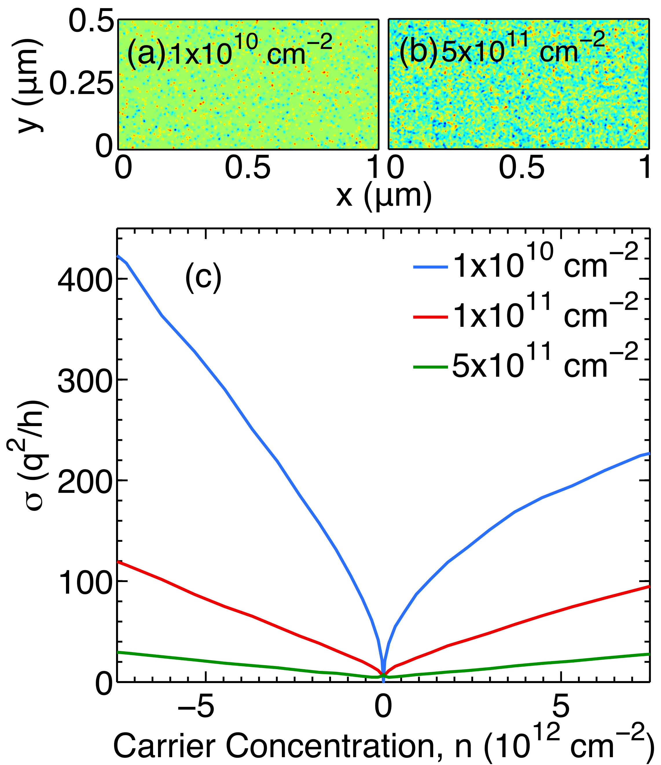
As a final example, we show how our model can interpolate between the ballistic and diffusive limits. We model the transport with impurity scattering by using a sequence of Gaussian potential profiles for the scattering centers [18], that specifies the strength of the impurity potential at atomic site . are the positions of the impurity atoms and is the screening length ( 3nm for long range scatterers). The amplitudes are random numbers following a Gaussian profile [19], is the impurity concentration. With added to (potential landscape shown in Fig. 4a-b), we study the evolution of electron transport in graphene from ballistic to diffusive (for varying . Fig. 4c shows the graphene conductivity at various channel carrier densities for several impurity concentrations. This time we keep the two ends of the graphene device at constant doping to capture the contact induced doping in graphene. This produces electron-hole asymmetry in the ballistic limit due to formation of junction near the contact. At high impurity concentration, the contact resistance becomes less dominant compared to the device resistance and the electron-hole asymmetry washes out, similar to what is seen in experiments [20]. Furthermore at the diffusive limit, becomes proportional to for a sample dominated by long range scatterers and can be fitted with a carrier density () independent mobility. As we lower the impurity concentration towards the ballistic limit, the graphene conductance () becomes proportional to the effective doping , leading to a sub-linear ), where the transmission is determined by the metal-graphene contact. Such an evolution of electron transport in graphene has been verified in experiments [21].
In conclusion, we have shown that for massless Dirac fermions, an additional quadratic term in the Dirac Hamiltonian not only circumvents the Fermion doubling problem in a spatial lattice but also has a huge computational advantage over the atomistic tight binding model. In particular, we have shown that the modified Hamiltonian results in an extremely small matrix on a real space square lattice. As a result, the Hamiltonian is orders of magnitude faster than the tight binding Hamiltonian when used in band structure and quantum transport simulations. We applied this Hamiltonian for micron scaled graphene devices to study magneto-transport and electron transport in ballistic and in diffusive limit. Although only graphene is considered here, it is applicable to any other Dirac materials like topological insulators and can be used to calculate the spin current [22] as well.
Acknowledgements.
This work was supported by the financial grant from the NRI-INDEX center.References
- [1] Q. H. Wang, K. Kalantar-Zadeh, A. Kis, J. N. Coleman, and M. S. Strano, Nature Nanotechnology 7, 699 (2012).
- [2] A. Mellnik et. al., arXiv preprint arXiv:1402.1124 (2014).
- [3] S. Z. Butler et. al., ACS nano 7, 2898 (2013).
- [4] S. Datta, Electronic Transport in Mesoscopic Systems (Cambridge University Press, 1997).
- [5] L. Susskind, Phys. Rev. D 16, 3031 (1977).
- [6] R. Stacey, Phys. Rev. D 26, 468 (1982).
- [7] S. Hong, V. Diep, S. Datta, and Y. P. Chen, Phys. Rev. B 86, 085131 (2012).
- [8] P. R. Wallace, Physical Review 71, 622 (1947).
- [9] T. Taychatanapat, K. Watanabe, T. Taniguchi, and P. Jarillo-Herrero, Nat Phys 9, 225 (2013).
- [10] M.-H. Liu, P. Rickhaus, P. Makk, E. Tóvári, R. Maurand, F. Tkatschenko, M. Weiss, C. Schönenberger, and K. Richter, Phys. Rev. Lett. 114, 036601 (2015).
- [11] K. Alam and R. K. Lake, Journal of applied physics 98, 064307 (2005).
- [12] R. N. Sajjad, C. A. Polanco, and A. W. Ghosh, Journal of Computational Electronics 12, 232 (2013).
- [13] R. N. Sajjad, S. Sutar, J. Lee, and A. W. Ghosh, Physical Review B 86, 155412 (2012).
- [14] M. I. Katsnelson, K. S. Novoselov, and A. K. Geim, Nat Phys 2, 620 (2006).
- [15] V. Tsoi, J. Bass, and P. Wyder, Reviews of Modern Physics 71, 1641 (1999).
- [16] M. Büttiker, IBM Journal of Research and Development 32, 317 (1988).
- [17] M. Galperin, S. Toledo, and A. Nitzan, The Journal of Chemical Physics 117, 10817 (2002).
- [18] J. W. Kłos and I. V. Zozoulenko, Phys. Rev. B 82, 081414 (2010).
- [19] Y. Sui, T. Low, M. Lundstrom, and J. Appenzeller, Nano letters 11, 1319 (2011).
- [20] M. J. Hollander, N. Shukla, N. Agrawal, H. Madan, J. A. Robinson, and S. Datta, in Device Research Conference (DRC), 2013 71th Annual (IEEE, 2013) pp. 151–52.
- [21] J.-H. Chen, C. Jang, S. Adam, M. S. Fuhrer, E. D. Williams, and M. Ishigami, Nat Phys 4, 377 (2008).
- [22] K. M. Habib, R. N. Sajjad, and A. W. Ghosh, Physical review letters 114, 176801 (2015).