Homes Scaling in Ionic Liquid Gated La2CuO4+x Thin Films
Abstract
Finding more efficient ways of exploring the doping phase diagrams of high temperature superconductors as well as probing the fundamental properties of these materials are essential ingredients for driving the discovery of new materials. We use a doping technique involving gating with ionic liquids to systematically and continuously tune the of superconducting La2CuO4+x thin films. We probe both the transport properties and the penetration depth of these samples and find that Homes scaling is obeyed, consistent with these materials being in the dirty limit. This result is independent of the precise mechanism for the gating process as all of the parameters of the scaling relationship are determined by direct measurements on the films.
pacs
74.72.-h, 74.78.-w, 74.62.-cThe study of high-temperature superconductivity is a field dating back to the discovery of LaBa2Cu3O7-x[1]. Since that time, there has been a steady drive to increase the transition temperature of these materials with the ultimate goal of finding a room temperature superconductor which could unlock many practical technologies. At a basic level this push for higher transition temperatures is a material search. Ionic liquids offer the exciting possibility of increasing the efficiency of this search, allowing one to explore a whole range of doping for a material system in a single sample, where previously a whole series of sample growths would be required. We demonstrate the use of ionic liquids in an electric double layer transistor configuration to continuously tune the transition temperature of superconducting La2CuO4+x (LCO) thin films. This allows us to precisely monitor how the change in the carrier concentration affects the transition temperature, resistance and superconducting penetration depth of the material. We highlight these details and demonstrate through the verification of Homes scaling[2] that that this approach is nevertheless a powerful alternative to chemical doping for systematically studying the properties of high-temperature superconductors. This is true despite the fact that the doping in this material may not be a purely electrostatic effect.
These films were grown by ozone-assisted molecular beam epitaxy [3]. We use Cu and La Knudsen effusion cells to produce stable rates for these two materials. The rate for each source is measured prior to the film growth using a quartz crystal microbalance. We alternately deposit one half of a unit cell of La then Cu by opening shutters for each source. The film presented here is 3 unit cells thick. The substrate temperature is 700 as measured by a Williamson Pro 92-38 pyrometer and under an ozone pressure of 3x10⁻⁵ torr during growth. We monitor the growth of the films using RHEED and see strong 2D film streaks epitaxially locked to the a and b axes of the substrate’s lattice. We use oriented SrLaAlO4 substrates supplied by MTI corp. The of the initial sample before the application of ionic liquid and gate voltage is well-defined and is greater than 40K, which is a sign of high quality and implies that the excess oxygen is near its maximal value of x=0.12.
Tuning the properties of high materials using a conventional FET configuration is a well established technique for systematically adjusting the carrier concentration of superconducting materials[4, 5, 6]. The use of ionic liquids to tune the properties of thin films has grown rapidly in the past several years due to the possibility of producing large changes in the carrier concentration of a material. Some of the first efforts in this regard were by Iwasa’s group [7]. In terms of studying high temperature superconductors, this technique has been applied to La2-xSrxCuO4[8], YBa2Cu3O7-x[9, 10], LCO[11] and Pr2-xCexCuO4 [12]. In all of these studies the focus was on the superconductor-insulator transition. The work presented here is an extension of that done on LCO with the technique of penetration depth measurements added in parallel with standard transport measurements. This combination allows us to determine the evolution of the relationships between various superconducting and normal state properties with applied gate voltage and temperature.
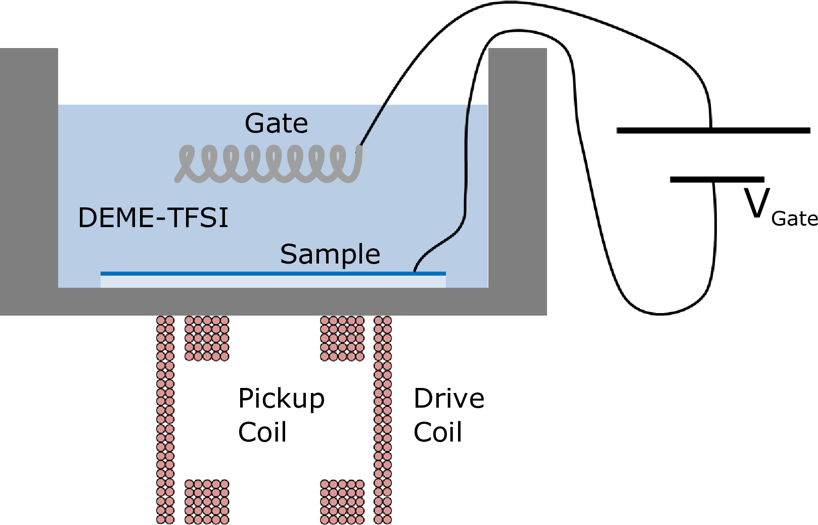
We used a two-coil mutual inductance technique for tracking the penetration depth [13, 14, 15, 16, 17]. The experimental setup is shown in Fig. 1. Both the drive and pickup coils are located on the back side of the sample. The holder is constructed out of Delrin. We use an SRS SR830 lock-in amplifier to both produce the drive signal and in conjunction with an SRS SR560 amplifier to measure the output from the pickup coil. The AC drive signal has a frequency of 50 kHz and an amplitude of 1 mA. We use a numerical procedure for determining the penetration depth of the sample from the measured real and imaginary components of the voltage read by the pickup coil. We model the film with a complex impedance, , where R and are the sheet resistance and the kinetic inductance of the film, respectively. In the case of a thin film with thickness d and , the kinetic inductance is directly related to the London penetration depth as , where is the permeability of free space and is the London penetration depth.
We used the ionic liquid DEME-TFSI to tune the properties of our superconducting samples. The ionic liquid is initially applied to the surface of the sample at room temperature but all further gating is done at 245 K. Figure 2 shows how the resistance, carrier concentration, and mobility evolve with the applied gate voltage at a temperature of 180K. All three quantities were determined using a 4-wire resistance technique in a Van der Pauw configuration. Each measurement step involves warming the sample and ionic liquid to 245 K, which is above the melting point of the liquid. The gate voltage is then changed at this elevated temperature and allowed to relax for 20 min. We apply a positive voltage to the gate, which corresponds to removing holes or reducing the number of charge carriers in the sample. As the gate voltage is increased we see both an increase in the resistance of the film and a decrease in the carrier concentration. While the mobility does begin to decrease at higher gate voltages we see that the primary effect of the applied voltage is to reduce the number of free holes in the material. We note that the gating procedure is not purely electrostatic as the changes upon gating are irreversible. The evidence for this conclusion comes from removing the applied gate voltage and observing that the resistance does not return to the zero-voltage state. In fact, we must apply a negative gate voltage in order to return the resistance to its initial state. There is evidence in many other material systems doped with ionic liquids showing that the gating process is often a mixture of electrochemical and electrostatic effects [18, 19, 20, 21]. Particular to LCO, there is evidence that the interstitial oxygens are mobile down to 200 K[22] and it would not be surprising to think that the ionic liquid gating procedure removing holes actually removed some oxygen. Now, while there are advantages to a purely electrostatic process, namely reversibility and no introduction of disorder, an in-situ electrochemical doping method, which we believe may be involved in the process presented here, is still a powerful and useful tool.


Due to imprecise knowledge of the distance between the coils and the sample, we cannot determine the absolute size of the penetration depth. Instead, to set the scale, we use 2700 Å based on literature values for La2-xSrxCuO4[23, 24, 25] a compound with a similar transition temperature, to calibrate the unknown spacing between the sample and the coils. We then measure changes in the penetration depth from that starting point as we adjust the doping of the sample using the gate electrode in the ionic liquid. The real and imaginary components of the voltage in the pickup coil are shown in Fig. 3. The real component has a peak centered at the superconducting transition and the width of the peak is, in part, a measure of the homogeneity of the sample at that doping. We see that with increasing applied gate voltage the peak moves to lower temperatures and broadens. We interpret this as a change in the doping of the material, removing holes, but not necessarily in a fully homogeneous way. We will use the center of this peak as our definition of for the purposes of checking the Homes scaling relation [2]. The imaginary component of the voltage, while not explicitly equal to it, represents the kinetic inductance of the sample which is directly related to both the penetrations depth and superconducting electron density. We see the imaginary component move to lower temperatures and go to zero with increasing gate voltage. Data on the resistance of the sample can be obtained in parallel with the two-coil signal. We see that as we increase the gate voltage and remove holes the normal state resistance increases and steadily decreases. We can translate the combination of real and imaginary components of the pickup coil signal into the penetration depth of the sample.
The first thing to check is the temperature dependence of the penetration depth. Depending on the pairing state of the superconductor we expect to have a specific temperature dependence. For an s-wave pairing state with a full gap we expect an exponential dependence for . For a d-wave pairing state, where there are nodes in the gap, we expect a linear dependence for . In the case of strong scattering this linear dependence shifts to [26]. We have seen (not shown) that this sample exhibits a quadratic temperature dependence, which implies scattering is playing a significant role. The ultra thin nature of this sample means that the upper and lower surface roughness make up a large fraction of the thickness of the entire film. We used both X-ray reflectivity (XRR) and atomic force microscopy (AFM) to characterize the film roughness. From XRR our estimates of the substrate-sample interface roughness and the sample surface roughness are 3 Å and 8 Å, respectively. Using AFM we measure the sample surface roughness to be 3 Å. All of these quantities are significant compared to the c-axis lattice parameter, which is 13.3 Å. Considering that the entire film thickness is 3 unit cells and the roughness of both of the top and bottom surface are significant fractions of a unit cell it is reasonable to expect this film to be in the strong scattering limit.
The next check we can make with this data set is to see if the Homes scaling relationship is obeyed[2, 27]. Figure 5 demonstrates that does in fact provide a good description of our data. We use the conductivity at 180 K and define using the peak value of the real component of the two-coil signal. Both of these are clearly defined values even when the transition becomes broad at higher gate voltages. The scaling relationship also holds when the conductivity just at the onset of superconductivity is employed. Following the work of Zuev et al.[28] we can use the relationship
| (1) |
to define , which is the Berezinskii-Kosterlitz-Thouless-transition temperature. Here is the flux quntum. If we use the entire film thickness of 40 Å as the value of we find good agreement between this definition of and the value of we determine from the peak of the real component of the two coil signal.
There are a number of different proposals for the interpretation of the relationship [29, 30, 31, 32]. The simplest argument comes from the fact that the film is in the strong scattering limit () to begin with. For our films we use a simple Drude model to estimate the scattering rate. Taking the values of and from Fig. 2 and the relationship we can calculate to be 1.3 eV, which is much larger than the superconducting gap in these types of materials [33]. It is important to note that while the Homes data set is a compilation of many samples measured over the course of many years, the data shown here is from a single sample continuously doped to cover a range of values in a systematic and efficient manner. This points to the power of using ionic liquids in an electric double layer transistor configuration to systematically study the fundamental properties of superconducting samples.


The initial motivation for exploring whether there is a fundamental relationship between and was derived from the empirical relationship proposed by Uemura et al. [34]. The data presented here does not follow the relationship proposed by Uemura of . This is actually readily seen by a more careful examination of Fig. 4. We see that the quantity , which is proportional to the superconducting electron density, increases linearly with the number of free carriers in the normal state. Simply, the number of superconducting electrons in the superconducting state is proportional to the number of free holes in the normal state. This means that we could simply switch the x-axis of Fig. 4 from doping (carrier concentration) to without effecting the shape of the curve. This means the relationship between and will just be a remapping of the superconducting dome and therefore not a linear function as seen by Uemura in other, chemically doped high- materials. There is precedent for a sub-linear relationship for , where a value of follows from an argument about critical scaling where there is a quantum critical point (QCP) at the edge of the dome[28, 25]. While we do see a sub-linear relationship (), it is not a pure single power law over the range of dopings examined here, much of which is likely far from the QCP point.
In summary, we have used the ionic liquid DEME-TFSI to systematically tune the transition temperature of under-doped LCO thin films, and have displayed and analyzed data from a 3-unit cell thick film. This has allowed us to carefully track how the resistance, Hall Effect, and penetration depth are interrelated. Our results are in good agreement with the Homes scaling relation consistent with the fact that this film is in the strong scattering limit. In addition, this unique setup allows us to explicitly show that the super-electron density, as measured by is linearly proportional to the free carriers in the normal state. As a result of this linear dependence we see that any fundamental relationship between and will just be a remapping of the superconducting dome. These results are independent of the precise mechanism associated with the doping process, which may in part be electrochemical, rather than purely electrostatic. This suggests that ionic liquid gating may be a powerful way to explore the phase diagram of other materials, and should be considered to be an effective complement to conventional chemical doping.
The authors would like to thank Rafael Fernandes and Peter Orth for useful discussions. This work was primarily supported by the National Science Foundation through the University of Minnnesota MRSEC under Award Number DMR-1420013 and partially supported by the National Science Foundation under Award Number DMR-1209578. Part of this work was carried out at the University of Minnesota Characterization Facility, a member of the NSF-funded Materials Research Facilities Network via the MRSEC program, and the Nanofabrication Center which receives partial support from the NSF through the NNIN program.
References
- [1] J. G. Bednorz and K. A. Müller, Zeitschrift für Physik B Condensed Matter 64, 189 (1986).
- [2] C. C. Homes, S. V. Dordevic, M. Strongin, D. A. Bonn, R. Liang, W. N. Hardy, S. Komiya, Y. Ando, G. Yu, N. Kaneko, X. Zhao, M. Greven, D. N. Basov, and T. Timusk, Nature 430, 539 (2004).
- [3] D. D. Berkley, B. R. Johnson, N. Anand, K. M. Beauchamp, L. E. Conroy, A. M. Goldman, J. Maps, K. Mauersberger, M. L. Mecartney, J. Morton, M. Tuominen, and Y.-J. Zhang, Applied Physics Letters 53, 1973 (1988).
- [4] D. Matthey, N. Reyren, J.-M. M. Triscone, and T. Schneider, Physical Review Letters 98, 057002 (2007).
- [5] M. Salluzzo, A. Gambardella, G. M. De Luca, R. Di Capua, Z. Ristic, and R. Vaglio, Physical Review B 78, 054524 (2008).
- [6] A. Rüfenacht, J.-P. P. Locquet, J. Fompeyrine, D. Caimi, and P. Martinoli, Physical Review Letters 96, 227002 (2006).
- [7] K. Ueno, S. Nakamura, H. Shimotani, A. Ohtomo, N. Kimura, T. Nojima, H. Aoki, Y. Iwasa, and M. Kawasaki, Nature materials 7, 855 (2008).
- [8] A. T. Bollinger, G. Dubuis, J. Yoon, D. Pavuna, J. Misewich, and I. Božović, Nature 472, 458 (2011).
- [9] X. Leng, J. Garcia-Barriocanal, S. Bose, Y. Lee, and A. M. Goldman, Physical Review Letters 107, 027001 (2011).
- [10] X. Leng, J. Garcia-Barriocanal, B. Yang, Y. Lee, J. Kinney, and A. M. Goldman, Physical Review Letters 108, 067004 (2012).
- [11] J. Garcia-Barriocanal, A. Kobrinskii, X. Leng, J. Kinney, B. Yang, S. Snyder, and A. Goldman, Physical Review B 87, 024509 (2013).
- [12] S. W. Zeng, Z. Huang, W. M. Lv, N. N. Bao, K. Gopinadhan, L. K. Jian, T. S. Herng, Z. Q. Liu, Y. L. Zhao, C. J. Li, H. J. Harsan Ma, P. Yang, J. Ding, T. Venkatesan, and Ariando, Physical Review B 92, 020503 (2015).
- [13] A. Hebard and A. Fiory, Physical Review Letters 44, 291 (1980).
- [14] B. Jeanneret, J. L. Gavilano, G. A. Racine, C. Leemann, and P. Martinoli, Applied Physics Letters 55, 2336 (1989).
- [15] Z.-H. Lin, G. C. Spalding, A. M. Goldman, B. F. Bayman, and O. T. Valls, Europhysics Letters (EPL) 32, 573 (1995).
- [16] S. J. Turneaure, E. R. Ulm, and T. R. Lemberger, Journal of Applied Physics 79, 4221 (1996).
- [17] S. J. Turneaure, A. a. Pesetski, and T. R. Lemberger, Journal of Applied Physics 83, 4334 (1998).
- [18] J. Jeong, N. Aetukuri, T. Graf, T. D. Schladt, M. G. Samant, and S. S. P. Parkin, Science (New York, N.Y.) 339, 1402 (2013).
- [19] J. Jeong, N. B. Aetukuri, D. Passarello, S. D. Conradson, M. G. Samant, and S. S. P. Parkin, Proceedings of the National Academy of Sciences 112, 1013 (2015).
- [20] A. C. Lang, J. D. Sloppy, H. Ghassemi, R. C. Devlin, R. J. Sichel-Tissot, J.-C. Idrobo, S. J. May, and M. L. Taheri, ACS Applied Materials & Interfaces 6, 17018 (2014).
- [21] T. A. Petach, M. Lee, R. C. Davis, A. Mehta, and D. Goldhaber-Gordon, Physical Review B 90, 081108(R) (2014).
- [22] M. Fratini, N. Poccia, A. Ricci, G. Campi, M. Burghammer, G. Aeppli, and A. Bianconi, Nature 466, 841 (2010).
- [23] T. Startseva, T. Timusk, A. V. Puchkov, D. N. Basov, H. A. Mook, M. Okuya, T. Kimura, and K. Kishio, Physical Review B 59, 8 (1998).
- [24] G. Aeppli, E. J. Ansaldo, J. H. Brewer, R. J. Cava, R. F. Kiefl, S. R. Kreitzman, G. M. Luke, and D. R. Noakes, Physical Review B 35, 7129 (1987).
- [25] T. R. Lemberger, I. Hetel, A. Tsukada, M. Naito, and M. Randeria, Physical Review B 83, 140507 (2011).
- [26] M. Prohammer and J. P. Carbotte, Physical Review B 43, 5370 (1991).
- [27] C. C. Homes, S. V. Dordevic, T. Valla, and M. Strongin, Physical Review B 72, 134517 (2005).
- [28] Y. Zuev, M. Seog Kim, and T. R. Lemberger, Physical Review Letters 95, 137002 (2005).
- [29] Y. Imry, M. Strongin, and C. C. Homes, Physical Review Letters 109, 067003 (2012).
- [30] V. G. Kogan, Physical Review B 87, 220507 (2013).
- [31] B. J. Taylor and M. B. Maple, Physical Review B 76, 184512 (2007).
- [32] D. N. Basov and A. V. Chubukov, Nature Physics 7, 272 (2011).
- [33] M. Hashimoto, I. M. Vishik, R.-H. He, T. P. Devereaux, and Z.-X. Shen, Nature Physics 10, 483 (2014).
- [34] Y. Uemura, G. Luke, B. Sternlieb, J. Brewer, J. Carolan, W. Hardy, R. Kadono, J. Kempton, R. Kiefl, S. Kreitzman, P. Mulhern, T. Riseman, D. Williams, B. Yang, S. Uchida, H. Takagi, J. Gopalakrishnan, A. Sleight, M. Subramanian, C. Chien, M. Cieplak, G. Xiao, V. Lee, B. Statt, C. Stronach, W. Kossler, and X. Yu, Physical Review Letters 62, 2317 (1989).