Modulated Helical Metals at Magnetic Domain Walls of Pyrochlore Iridium Oxides
Abstract
Spontaneous symmetry breakings, metal-insulator transitions, and transport properties of magnetic-domain-wall states in pyrochlore iridium oxides are studied by employing a symmetry adapted effective hamiltonian with a slab perpendicular to the (111) direction of the pyrochlore lattice. Emergent metallic domain wall, which has unconventional topological nature with a controllable and mobile metallic layer, is shown to host Fermi surfaces with modulated helical spin textures resembling Rashba metals. The helical nature of the domain-wall Fermi surfaces is experimentally detectable by anomalous Hall conductivity, circular dichroism, and optical Hall conductivity under external magnetic fields. Possible applications of the domain-wall metals to spin-current generation and “half-metallic” conduction are also discussed.
I Introduction
Emergent quantum phases of pyrochlore iridium oxides Ir2O7 (R: rare-earth elements) have attracted broad interest [1, 2, 3, 4, 5]. Previous theoretical studies have predicted Weyl semimetals in non-collinear magnetic phases of Y2Ir2O7 [4], and non-Fermi-liquid ground states [6, 7, 8, 9] or strong topological insulators as spontaneously symmetry breaking phases [10, 11, 12, 13, 14] in a paramagnetic pyrochlore iridium oxide Pr2Ir2O7.
The non-collinear magnetic phase called the all-inall-out (AIAO) phase, which was theoretically predicted for Y2Ir2O7 [4] and experimetally confirmed for Nd2Ir2O7 [15] and Eu2Ir2O7 [16], shows other possible intriguing transport properties [17, 18]. For example, thin films of the pyrochlore iridium oxides with the AIAO orders have been proposed to exhibit anomalous Hall effects [19]. The authors have predicted that magnetic domain walls in the AIAO phase host metallic domain-wall states characterized by a zero-dimensional class A Chern number [20].
Magnetic domain walls have been an ingredient of spintronics. [21] In both of old-fashioned magnetic bubble memories and cutting-edge magnetoresistive random access memories, magnetic domains themselves have conveyed information. In contrast, while the domains in the AIAO orders of the pyrochlore iridium oxides themselves remain functionless magnetic insulators, the magnetic domain walls in the AIAO phases have been predicted to offer tunable, controllable and mobile two-dimensional metallic layers [20].
In the present paper, we clarify the functions of the predicted topological domain-wall metals of the pyrochlore iridium oxides in more details. First, spontaneous symmetry breakings and metal-to-insulator transitions at the magnetic domain walls are examined. A single (111) magnetic domain wall in a simple tight binding model for the pyrchlore iridium oxide with spin-orbit couplings is studied by employing a slab geometry perpendicular to the (111) direction and an unrestricted Hartree-Fock approximation. Next, the transport properties of the (111) domain wall are studied by using the Kubo formula. Anomalous and optical Hall conductivities characterize the domain-wall metals.
We show that the domain-wall metals are characterized by modulated helical two-dimensional Fermi surfaces. Resembling Rashba-split Fermi surfaces [22, 23, 24] observed, for example, in surface states of noble metals [25], inverted semiconductor heterostructures [26], and, recently, in a bulk semiconductor BiTeI [27], spin/total-angular-momentum polarization tangential to Fermi surfaces is realized in the modulated helical Fermi surfaces. Differently from intensively studied ideal helical Fermi surfaces of topological insulator surfaces [28, 29, 30], which are described by a Dirac hamiltonian , the spin/total angular moment of electrons are affected by trigonal warpings and have their components perpendicular to the two-dimensional plane.
We also show that there are two categories of domain wall metals, namely, helical metals with and without degeneracy: Degenerate helical metal is characterized by the two-fold degeneracy of the Fermi surface states at every momenta and the helical metal emerges by a spontaneous symmetry breaking of this degeneracy leading to the emergence of a magnetic moment at the domain wall and the splitting of the two-fold degenerate Fermi surface, which emerges as a first-order transition and is evidenced by sudden changes in the anomalous Hall conductivities of the domain-wall metals and the jump in the density of states at the Fermi level. Splittings of the modulated helical Fermi surfaces eventually lead to a metal-to-insulator transition when the ratio of the intra-atomic Coulomb repulsions and the kinetic energy is further increased by applying negative chemical or physical pressures. The absolute value of the anomalous Hall conductivity itself, however, is extremely sensitive to boundary conditions.
We also propose that the optical Hall conductivity offers an experimental hallmark of the degenerate helical domain-wall metals. In contrast to the optical Hall conductivities due to the formation of Landau levels, the imaginary part of the optical Hall conductivity of the degenerate helical metals show a continuum of optical Hall responses with a finite width proportional to Zeeman energy and, hence, proportional to external magnetic fields.
The organization of the present paper is the following. In this paper, we focus on magnetic domain walls in a Hubbard-type effective hamiltonian of electrons in =1/2-manifold of iridium atoms that constitute a pyrochlore lattice. The effective hamiltonian is introduced in Sec. II. With a slab geometry, electronic and transport properties of a single magnetic domain wall of Ir2O7 are studied by employing the unrestricted Hartree-Fock approximation and the Kubo formula, which are also described in Sec. II. The quantum phase transitions of the domain-wall metals are examined in Sec. III. Section IV and V are devoted to detailing the electronic and transport properties of the domain-wall metals. The weak topological nature proposed in Ref. 20 and possible application of the domain-wall metals are discussed in Sec. VI. Section VII is devoted to a summary of the present paper.
II Model and Method
II.1 Simple effective hamiltonian for electrons in =1/2-manifold
As a simple effective hamiltonian of pyrochlore iridium oxides, Ir2O7, we study the following effective Hubbard-type hamiltonian of electrons in =1/2-manifold of iridium atoms [3, 31, 14, 20] on a pyrochlore lattice (see the upper panel of Fig.1),
| (1) | |||||
where a fermionic operator () creates (annihilates) an electron with -spin at -th site. Here, is a vector consisting of Pauli matrices, is a vector from -th site to -th site, and is a vector from the center of the tetrahedron including -th and -th sites to the center of the bond connecting -th and -th sites (see the lower panel of Fig.1 that illustrates the directions of , , and ). In the above hamiltonian, the spin-orbit couplings are decoded as spin-dependent complex hoppings proportional to .
The previous studies have shown that, for , , and , the experimentally observed AIAO order is accounted for by the strong coupling expansion of Eq.(1) at half filling: The second order terms proportional to lead to the direct Dzyaloshinskii-Moriya (DM) interactions that are known to stabilize AIAO orders [32, 33, 34]. The DM interactions determine not only the mutual angles of the neighboring atoms’ magnetic moments but also the directions of these magnetic moments. In the strong coupling limit, the magnetic moments of the effective hamiltonian effectively feel Ising-like anisotropy through the exchange coupling.
Due to the effective Ising-like anisotropy, quantum and thermal fluctuations are suppressed and the mean-field treatments are basically justified deeply inside the AIAO orders. Thanks to the suppression, the unrestricted Hartree-Fock approximation becomes reasonable, which we employ in this paper, as introduced below.
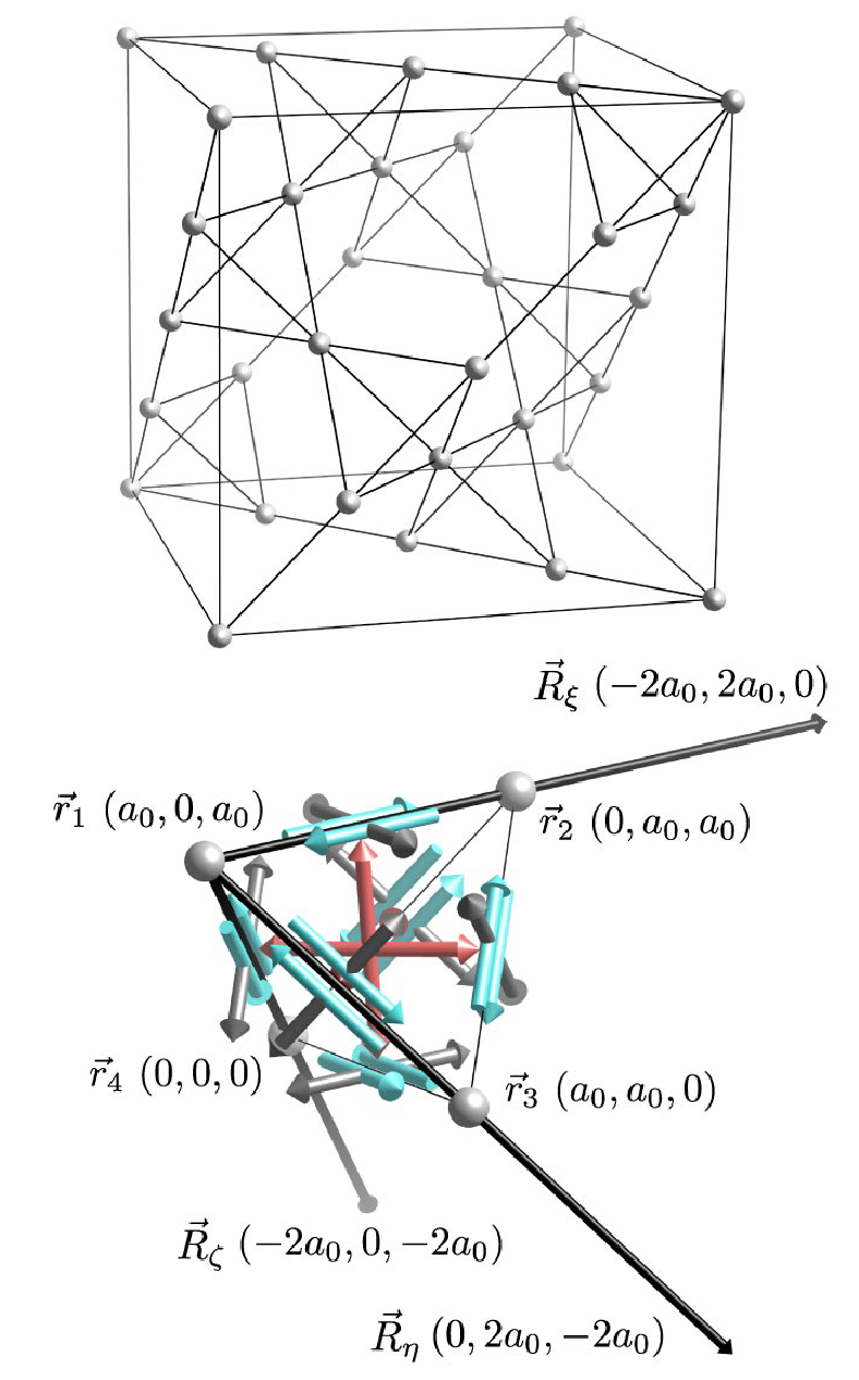
II.2 Slab geometry
To study magnetic domain walls of the pyrochlore iridium oxides Ir2O7, we introduce a slab with surfaces perpendicular to the (111) direction. The slab consists of regularly stacked Kagom and triangular layers. Here, we assume the translational symmetry along the Kagom and triangular layers perpendicular to the (111) direction for simplicity. Then, the slab is described as a two dimensional lattice with a unit cell that contains iridium atoms at
| (2) |
where is the site index inside a single tetrahedron, is the layer index, is defined with the distance between nearest neighboring iridium atoms (see also Fig.1) as
and is a lattice vector of bulk pyroclore lattices, which runs along the direction from to . The two dimensional lattice is defined by the lattice vectors and . Then, the top (bottom) surface of the slab is the Kagom (triangular) layer (see Fig.1).
We will show transport properties of the (111) magnetic domain walls later. To define the transport coefficients of the domain-wall states, here, we introduce an additional Cartesian coordinate with the axes , , and are parallel to , , and , respectively.
II.3 Unrestricted Hartree-Fock approximation
Here, we employ the unrestricted Hartree-Fock approximation, to describe the AIAO phases and magnetic domain walls by using the effective hamiltonian Eq.(1).
We decouple the Hubbard interaction terms in by introducing mean fields as,
| (6) | |||||
where the mean fields are defined as
| (7) | |||||
| (8) | |||||
| (9) | |||||
| (10) |
We do not introduce any restrictions on these self-consistent mean fields and .
II.4 Kubo formula
By employing the unrestricted Hartree-Fock approximation, the hamiltonian is reduced to the following general one-body hamiltonian,
| (11) |
where lowercase Roman letters () specify the site and spin indices of electrons, and represents two dimensional lattice momenta perpendicular to the (111) direction. In general, the one-body hamiltonian is diagonalized by introducing an unitary matrix as,
| (12) |
where lowercase Greek letters such as label eigenstates of and is the corresponding eigenvalue of .
We calculate the transport properties of by using the Kubo formula. In the present paper, we focus on charge conductivities defiend below. By using the charge current operators
| (13) |
is given from the Kubo formula [35, 36] as
| (14) |
where the Drude part is given as
| (15) |
and the area of the surface of the slab with unit cells is given as , is the inverse temperature, and is the Fermi distribution function. In this paper, we focus on zero temperature properties by taking sufficiently large.
III Domain-wall Phase Diagram
By employing the unrestricted Hartree-Fock approximation, we calculate physical properties of (111) magnetic domain walls of the effective hamiltonian Eq.(1) with a typical value of , , and a slab geometry with 40 layers (). Starting with an initial condition where all-out (all-in) magnetic moments for the -th tetrahedron for (), we obtain domain-wall solutions as local minima of the free energy.
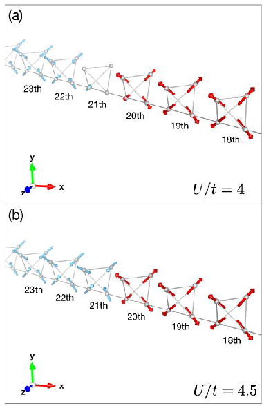
As examples of the domain-wall solutions, we illustrate the magnetic moments in Fig.2 at and . At , the domain-wall solution is symmetric under an inversion around one of the Kagom-plane sites taken together with the time reversal operation , as is shown in an example of Fig.2(a), where the 21st layer is the symmetric plane, if effects of surfaces of the slab with a finite thickness are neglected. On the other hand, this -symmetry is spontaneously broken at , which is evident in evolution of the magnetization at the Kagom-plane sites of the 21st layer. Later, the magnetization at the 21st Kagom plane is denoted as the domain-wall magnetization in comparison with the bulk magnetization practically defined as the magnetization at the 10th or 30th layer.
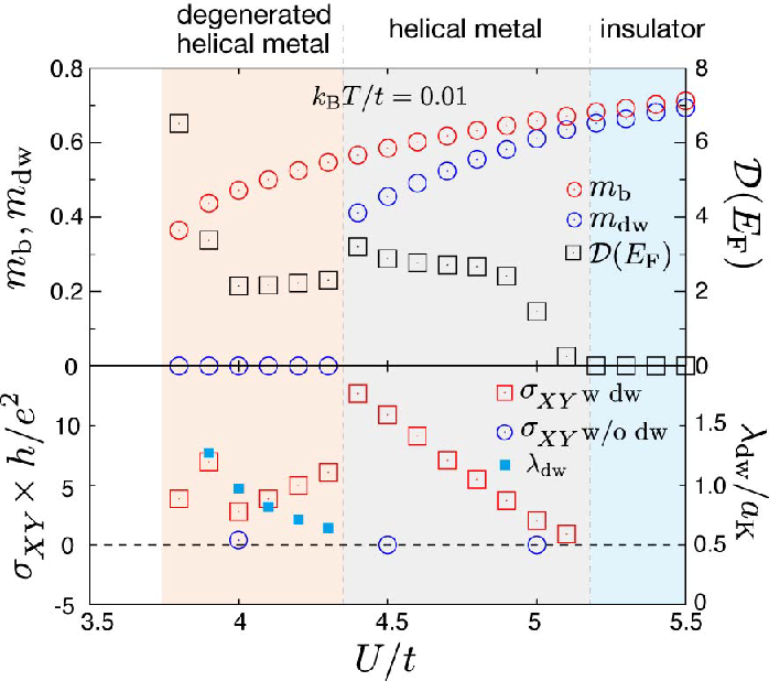
There are actually three phases for the domain-wall states, a degenerate helical metal, a helical metal, and an insulator. The phase transition between the degenerate helical and helical metals is of first order accompanied by the spontaneous symmetry breaking of the -symmetry in the helical-metal phase, The metal-to-insulator transitions at the domain walls are determined by the distinction between zero and nonzero densities of states at the Fermi level , , which is given as
| (16) |
The -dependences of , , and are summarized in the upper panel of Fig. 3.
In the lower panel of Fig. 3, we summarize anomalous Hall conductivities of the two-dimensional domain-wall metals and domain-wall thickness defined through fitting the sublattice magnetization with , where is a distance from the 21st Kagom layer measured along the (111) direction. The anomalous Hall conductivities for a slab with a single domain wall and without any domain walls are shown in the lower panel of Fig.3. In the -dependence of with a single domain wall, the first order phase transition between the degenerate helical metals and the helical metals is evident as a jump in . The domain-wall thickness can be fitted only in the degenerate helical metals with the vanishing magnetization , while the width of the domain wall is practically zero in the helical metal and insulator phases. For , the domain-wall structures are not characterized by an assumption .
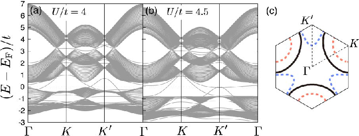
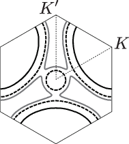
We next show the band structures of the degenerate helical metals and the helical metals in Fig.4. First of all, as naturally expected, there are no significant differences in the overall bulk band dispersion for and as shown in Fig.4(a) and (b), except for the bulk charge gaps, and the bands associated with the domain-wall and surface. Ingap bands with band bottoms at the point are surface bands of the slab. The broken inversion symmetry (or the differences between the and points) of the slab in the AIAO phase is detectable in the domain-wall and surface states. In contrast to the bulk band dispersion, the spontaneous -symmetry breakings at the domain wall is evident in the domain-wall Fermi surfaces shown in Fig.4(c). Here, the -symmetry breaking is evidenced from the split Fermi surfaces centered at the and pionts, while these two Fermi surfaces are degenerated in the degenerate helical metals.
In the degenerate helical metals, the Fermi surfaces consist of degenerated hole pockets centered at the point. On the other hand, in the helical metals, the Fermi surfaces consist of a hole pocket centered at the point and an electron pocket centered at the point. The impact of the broken -symmetry is significant in the electron pocket centered at the point. In the evolution from the degenerated hole pocket centered at the point to the electron pocket centered at the point with increasing , there should be changes in topology of the Fermi surface, as illustrated in Fig.5. Starting with the hole pockets centered at the point obtained in the degenerate helical metals, by increasing the hole density for the band that forms one of the hole pockets, a hole pocket centered at the point is also created. For further increase in the hole density, the newly-created hole pocket around the point and the original hole pocket around the point touch each other. Then, a closed electron-like Fermi surface enclosing the point appears through a Lifshitz transition[37]. Due to the changes in the Fermi surface topology, namely the Lifshitz transition, the -symmetry breakings become of first order [38].
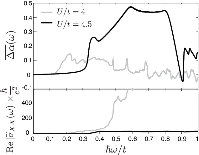
Before going into distinct natures of degenerate helical and helical metals, which will be discussed in the following sections, we show that the helical natures of these metallic states are evident in absorption of cicularly polarized light: Circular dichroism appears in absorption of cicularly polarized light incident along the (111) direction on the domain walls, in both of degenerate-helical- and helical-metal phases. If we choose eV by comparing the band width of the present hamiltonian with LDA results for Y2Ir2O7 [4], we predict experimentally detectable circular dichroism in mid-wavelength or far infrared region.
In two-dimensional metals, the plasma frequency at small momentum is proportional to . The simple Drude model for optical properties of single-band two-dimensional metals [39], therefore, predicts optical transparency. Even for the three dimensional systems, if the thickness of the metallic layers is negligible, the intraband optical response becomes vanishing. Consequently, the optical absorption of electromagnetic waves at the magnetic domain walls is expected to be governed by and proportional to the interband components of optical conductivities [40]. Here, we examine the circular dichroism through non-Drude part of optical conductivities for the circularly polarized light . To obtain , we replace with and set in Eq.(14), where .
As an index to measure the circular dichroism, we choose a relative difference between and , defined as
| (17) |
It shows substantial amplitudes of around the optical absorption edge, as we see in Fig.6 (upper panel) in comparison with interband components of (lower panel).
IV Degenerate Helical Metals
In this section, we further clarify the nature of the degenerate helical metals. First, we examine the spin polarization on the degenerated Fermi surfaces. Next, we propose that the existence of the degenerate helical metals can be evidenced in experiments by their characteristic frequency and magnetic-field dependences of the optical Hall conductivities.
IV.1 Spin polarization on Fermi surfaces
In this subsection, we show the nature of the spin alignments on the Fermi surface of the domain wall states. First, we note that the degenracy of the eigenstate of is determined by the symmetry for the spin on the Fermi surface, instead of the SU(2) symmetry seen in Fermi surfaces of usual paramagnetic metals.
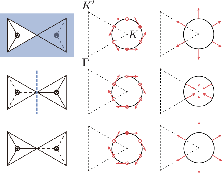
This is intuitively understood from the simultaneously satisfied symmetry and the symmetry derived from a set of succesive two mirror operations, both of which are preserved around the domain wall as is easily seen from the magnetic structure of the AIAO domain wall as detailed below by using the illustrations in Fig.7.
In the top panels of Fig.7, we decompose the spin into the out-of-plane (namely, along (111) direction) and the in-plane components by referring to the domain-wall plane, where the in-plane component is further decomposed into the component tangential to the Fermi surface (more precisely the Fermi line) and that perpendicular to the Fermi line in the two-dimensional Brillouin zone.
Let us first examine the degeneracy derived from the symmetry: We first show that the symmetry itself does not sufficiently restrict the direction of the spin on the Fermi surface. The operation simply requires that, by this operation, all the spin components are transformed to the opposite directions. The constraint is that the degenerate two states must have this spin inversion property.
However, the domain wall of the AIAO phase preserves another symmetry determined by the successive two mirror operations illustrated step by step in the left three panels of Fig. 7 from the top to the bottom. By this operation, the out-of-plane and tangential components of the spin are transformed to the opposite direction at least at the points where the Fermi surface (Fermi line) crosses the symmetry lines denoted by the -, -, and - lines. This inversion is the same as the operation (see the bottom middle panel of Fig. 7). However, in contrast to the operation, the component perpendicular to the Fermi surface within the domain-wall plane is unchanged under this operation as is seen in the bottom right panel of Fig.7. Therefore, the two symmetries are compatible only when the in-plane component perpendicular to the Fermi surface vanishes. This imposes a constraint that the in-plane component of the spin has only the tangential component at least in the illustrated symmetry points in the Brillouin zone.
Since the spin direction is inverted by the and the two-mirror-plane operations, the spin degeneracy follows the symmetry at each point of the Fermi surface. At the different points on the Fermi surface, the continuity of the spin direction is necessary along the Fermi surface to lower the energy. The spin-orbit interaction indeed preserves the two-fold degeneracy of clock-wise and anti-clock wise direction of the helicity shown in Fig.7, and the total symmetry emerges.
In other words, a generalization of Kramers degeneracy originating from the and two-mirror symmetries of the domain-wall states, instead of the time-reversal symmetry, guarantees the two-fold degeneracy of the eigenvalues of the one-body hamiltonian at . The invariance of under the operation of and the two succesive mirror operations requires that they map an eigenstate onto another eigenstate with the same eigenvalues. By noting that every single-particle eigenstate is a linear combination of orbitals and states are not invariant under the operation of , the eigenstates of are generically mapped onto another eigenstate different from the original states under the operation of .
By employing a realization of a operation, , we can write down the generalized Kramers degeneracy explicitly as,
| (18) |
and
| (19) |
where is a U(1) gauge of the wave function. Then, we formulate an assumption that the real-space wave functions of the domain-wall states are asymmetric around the inversion center of . The assumption is simply formulated as
| (20) |
The exclusion of the spin polarization perpendicular to the Fermi surface (Fermi line) clearly excludes a possibility that the domain-wall metals are simple paramagnetic metals. It is a natural consequence since, due to the strong spin-orbit couplings, the original SU(2) symmetry of the electrons’ spin is absent in the present system.
IV.2 An experimental hallmark of degenerate helical metals
The tangential spin polarization introduces opposite helicities for the two degenerated Fermi lines. The helicity inspires us to examine optical responses to incident light with circular polarization. Indeed, by calculating the optical Hall responses, we found that the low frequency behaviors of the optical Hall conductivities under external magnetic fields are different from those of paramagnetic metals.
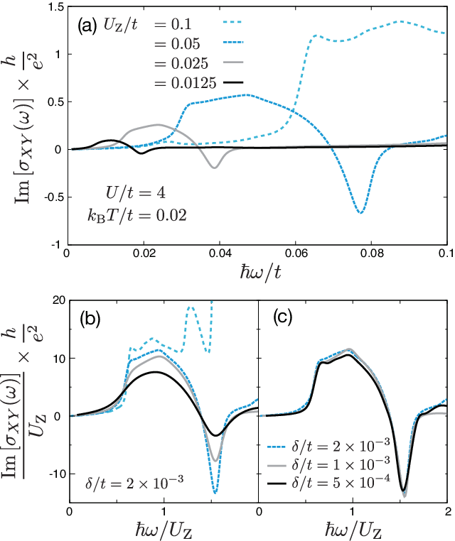
The calculated imaginary part of the optical Hall conductivities are shown in Fig.8 for . In Fig.8(a), we show the low frequency behaviors of under external magnetic fields parallel to the (111) direction. The effect of the magnetic fields is taken into account only through the Zeeman term, because, as we discuss later the effect from coupling through the electronic orbital motion is one order of magnitude smaller than the Zeeman effect, if we assume the electron effective mass in the order of with being the bare electronic mass, as is anticipated from the bandwidth of the LDA calculation[4, 41]. By changing the Zeeman term,
| (21) |
where is the Zeeman energy, the absorption continuum in the optical Hall conductivity shifts its location and width in frequency. Here, the Zeeman energy for Ir2O7 is estimated as
| (22) |
where () is a total magnetic moment (-factor) of an electron in -manifold, is the Bohr magneton, is an exchange coupling between an iridium atom and the 6 neighboring atoms, and is the magnetic moment of the atoms under external magnetic fields . We note that the simplified isotropic exchange coupling is employed, instead of the exchange couplings based on the symmetries of the wave functions of ions [42, 43]. By rescaling the imaginary part of and with the Zeeman energy , in Fig.8(b), we show that the width of the continuum is proportional to the Zeeman energy . Due to the finite line width introduced in Fig.8(a) and (b), , the detailed structures of the continua are smeared. To clarify the intrinsic structures of the continua, we change for each value of the Zeeman energy with keeping the ratio of the Zeeman energy and , as shown in Fig.8(c). For three different values for the Zeeman energy , the low frequency parts of are nearly collapsed into a single curve. The collapse indicates that the amplitudes of are also scaled with the Zeeman energy .
In usual metals, the imaginary part of the optical Hall conductivity arises due to the formation of the Landau levels. When the Landau levels induce the absorption in the optical Hall responses, the absorption spectra consist of sharp peak structures, instead of forming continua. In addition, under stronger external magnetic fields, the peak width is expected to remain unchanged or to become narrower. It is in sharp contrast with the present results.
Aside from the absorption peak shapes, the energy scale of the absorption spectra in the degenerate helical metals is distinct from that of usual paramagnetic metals. While the energy scale of the absorption continuum is governed by the Zeeman energy , optical transitions between the Landau levels are governed by the cyclotron frequency,
| (23) |
where is the effective mass of the domain-wall states and is the electron mass. In the present domain-wall states, we roughly estimate . Therefore, we expect that there are two distinct energy scales in optical Hall spectra, namely, the Zeeman energy and the cyclotron mass , which is roughly one order of magnitude smaller than . The expected separation of these two energy scales enables us to distinguish helical metals and ordinary paramagnetic metals.
For experimental observation, we roughly examine the energy scales of the frequency and the required magnetic fields. Here, by comparing the band width with pyrochlore iridium oxides and that of the effective hamiltonian, we estimate the energy scale as eV. Therefore, the relevant frequency range for the experimental observation revealed in Fig. 8(a) is up to 10 meV and the amplitude of external magnetic fields is up to T. The requirement for the external magnetic fields is seemingly demanding. However, in the pyrochlore iridium oxide with Nd, for example, the Zeeman fields originating from the magnetic moment of Nd atoms, , assist the external magnetic fields in enhancing the Zeeman splitting of the degenerated helical Fermi lines. Thus, we expect that external magnetic fields up to several T are enough for detecting the characteristic optical Hall responses discussed above in Nd2Ir2O7.
V Helical Metals
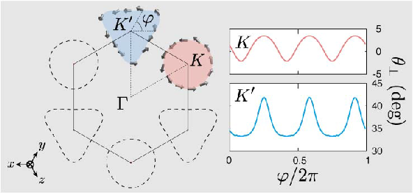
The spontaneously broken -symmetry induces split Fermi lines with spin polarization tangential to the Fermi lines with additional components parallel to the (111) direction. The explicit patterns of the spin polarization on the Fermi surfaces are given in Fig.9 for . As we mentioned in Fig.4, a hole pocket around the point and the electron pocket around the point emerge.
Here, to illustrate the spin polarization quantitatively, we introduce spin-resolved spectral weights. For example, the -component of the spin-resolved spectral weight is given by
where is a subsystem consisting of 19th, 20th, 21st, and 22nd layers including a single domain wall.
VI Discussion
VI.1 Weak topological nature
One might suspect that the emergence of insulating domain-wall states is inconsistent with the existence of the 1D hidden weak Chern number proposed in Ref.20. The hidden topological nature is based on symmetry of the eigenstates of the mean-field hamiltonian with a single AIAO magnetic domain wall: The eigenstates at the point are invariant or constituting two-dimensional irreducible representation under rotational symmetry around the (111) axis. The eigenvalues of the rotation classify these eigenstates at the point into three categories. Then, the number of the eigenstates in each categories gives us zero-dimensional Chern number. When the (111) domain walls are shifted by a unit layer along the (111) direction, the zero-dimensional Chern number is required to change. The changes in the Chern number require the existence of the ingap domain-wall states. In addition to the hidden Chern number, the symmetry of the AIAO domain walls in the degenerated helical metal phases guarantee the existence of the metallic domain-wall states. However, in the helical metal phase and beyond (see Fig3. for the phase diagram), the symmetry is broken and the topological protection is not guaranteed any more.
Even in the insulator phase, the insulating nature is fragile: if the domain walls are deformed and translated by a single layer with keeping rotational symmetry around the (111) axis, the changes in the zero dimensional Chern number require that the two domain-wall bands touch each other at the point, at least, once during the deformation. In other words, the mutual touching of these domain-wall bands changes the zero dimensional Chern number. This asserts that the insulating phase may have gapless metallic conduction to some extent with “bad insulating” nature when the domain walls are not strictly flat, for example.
VI.2 Memory effects in Hall measurements
Insertion of magnetic domain walls affects Hall conductivity, as evident in comparison between the Hall conductivity of a single domain slab and a slab with two domains that is separated by a single domain wall (Fig.3). Therefore, hysteresis due to insertion and removal of magnetic domain walls in Ir2O7, which is observed in magnetoresistivity [44, 45, 46], inevitably accompanies hysteresis in Hall conductivity.
VI.3 Spin current generation by charge current injection
In the helical-metal phase of the domain wall, there are a hole pocket centered at the point and an electron pocket centered at the point with modulated helical spin polarizaton. These two helical Fermi pockets stimulate interest in possible application to spintronics devices.
As same as the Rashba metals, spin polarization of electronic and hole carriers generated by charge current injection are anti-parallel if the Fermi velocity of these carriers are along the same direction, leading to the cancellation of the spin current for the contribution from the same Fermi velocity. However, due to lack of the -symmetry at the domain walls, the Fermi velocities of the hole carriers around the point and electron carriers around the point are, in general, different. Consequently, the difference in the Fermi velocities of two type of carriers generates spin currents under the external charge current injection. In the present simple tight-binding hamiltonian, the difference is significant, as seen in the band dispersion of the helical metals in Fig.4(b).
VI.4 “Half-metals” from lightly-doped domain-wall insulators
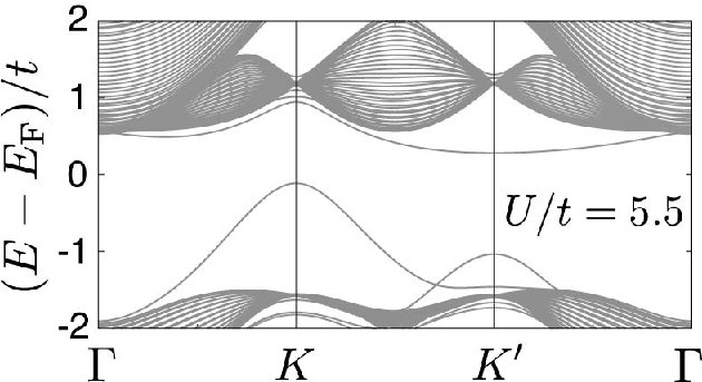
Finally, we discuss about a possible functionality of the domain-wall insulators in Ir2O7. As briefly explained below, lightly doped domain-wall insulators are expected to have a property equivalent to half metals.
In the insulating phases for (see the phase diagram shown in Fig.3), the top (bottom) of the hole (electron) band is located at the () point. In Fig.10, the slab band dispersion is shown for as an example of the insulating domain-wall states. At the both symmetric points in the Brillouin zone of the domain-wall states, the rotational symmetry around the (111) direction guarantees the full spin polarizations of the Bloch state along the (111) direction, at the two points: The invariance of the and under the rotation around the (111) axis prohibits the spin polarization within the (111) plane that breaks the invariance under the rotation. Therefore, if electronic or hole carriers are doped slightly into the domain walls, the doped carriers in the domain-wall insulators become completely spin polarized in the (111) direction, which is equivalent to electronic or hole half metals, respectively.
VII Summary
Quantum phase transitions, electronic and transport properties of domain-wall states of all-inall-out magnetic orders in pyrochlore lattice iridium oxides Ir2O7 (: rare-earth elements) are studied by using a symmetry adapted Hubbard-type hamiltonian of =1/2-manifold in the present paper. There exist three quantum phases at the magnetic domain walls: Metallic phases with degenerated helical Fermi surfaces, metals with helical electronic and hole Fermi pockets, and insulators appear at the domain walls depending on the ratio of the intra-atomic Coulomb repulsion to the nearest-neighbor hopping matrix . Gapless charge excitations in the degenerated helical metals are guaranteed by degeneracy due to -symmetry of the self-consistent domain-wall solutions combined with the existence of a weak one-dimensional Chern number, which is defined at the point of the domain-wall Brillouin zone. Experimental hallmarks of the degenerated helical metals are also examined. Spin polarization on the Fermi surfaces in the degenerated helical and helical metals is detailed by employing the double group symmetry of the domain walls and by showing direct numerical results. Possible applications of these domain-wall states such as spin current generation in the helical metals and half-metallic-like properties of lightly doped domain-wall insulators are also discussed.
Acknowledgements.
The authors thank Kentaro Ueda, Taka-hisa Arima, and Yoshinori Tokura for fruitful discussion. We acknowledge the financial supports by a Grant-in-Aid for Scientific Research (Grants No. 22104010 and No. 22340090) from MEXT, Japan. Y. Y acknowledge the financial supports by a Grant-in-Aid for Young Scientists (B) (Grant No. 15K17702) from MEXT, Japan. This work was also supported by the Strategic Programs for Innovative Research (SPIRE), MEXT conducted by the RIKEN Advanced Institute for Computational Science (AICS) (Grants No. hp130007 and hp140215) and Computational Materials Science Initiative (CMSI), Japan. The lattice structure and magnetic moments were visualized using VESTA 3 [47].References
- [1] D. Yanagishima and Y. Maeno, Journal of the Physical Society of Japan 70, 2880 (2001).
- [2] K. Matsuhira, M. Wakeshima, Y. Hinatsu, and S. Takagi, Journal of the Physical Society of Japan 80, 094701 (2011).
- [3] D. Pesin and L. Balents, Nature Physics 6, 376 (2010).
- [4] X. Wan, A. M. Turner, A. Vishwanath, and S. Y. Savrasov, Phys. Rev. B 83, 205101 (2011).
- [5] W. Witczak-Krempa, G. Chen, Y. B. Kim, and L. Balents, Annual Review of Condensed Matter Physics 5, 57 (2014).
- [6] A. A. Abrikosov and S. D. Beneslavskii, Sov. Phys. JETP 32, 699 (1971).
- [7] E.-G. Moon, C. Xu, Y. B. Kim, and L. Balents, Phys. Rev. Lett. 111, 206401 (2013).
- [8] I. F. Herbut and L. Janssen, Phys. Rev. Lett. 113, 106401 (2014).
- [9] L. Savary, E.-G. Moon, and L. Balents, Phys. Rev. X 4, 041027 (2014).
- [10] S. Raghu, X.-L. Qi, C. Honerkamp, and S.-C. Zhang, Phys. Rev. Lett. 100, 156401 (2008).
- [11] K. Sun, H. Yao, E. Fradkin, and S. A. Kivelson, Phys. Rev. Lett. 103, 046811 (2009).
- [12] Y. Zhang, Y. Ran, and A. Vishwanath, Phys. Rev. B 79, 245331 (2009).
- [13] J. Wen, A. Rüegg, C.-C. J. Wang, and G. A. Fiete, Phys. Rev. B 82, 075125 (2010).
- [14] M. Kurita, Y. Yamaji, and M. Imada, Journal of the Physical Society of Japan 80 (2011).
- [15] K. Tomiyasu, K. Matsuhira, K. Iwasa, M. Watahiki, S. Takagi, M. Wakeshima, Y. Hinatsu, M. Yokoyama, K. Ohoyama, and K. Yamada, Journal of the Physical Society of Japan 81, 034709 (2012).
- [16] H. Sagayama, D. Uematsu, T. Arima, K. Sugimoto, J. J. Ishikawa, E. O’Farrell, and S. Nakatsuji, Phys. Rev. B 87, 100403 (2013).
- [17] K.-Y. Yang, Y.-M. Lu, and Y. Ran, Phys. Rev. B 84, 075129 (2011).
- [18] V. Aji, Phys. Rev. B 85, 241101 (2012).
- [19] B.-J. Yang and N. Nagaosa, Phys. Rev. Lett. 112, 246402 (2014).
- [20] Y. Yamaji and M. Imada, Phys. Rev. X 4, 021035 (2014).
- [21] S. Parkin, Spin Dependent Transport in Magnetic Nanostructures, edited by S. Maekawa and T. Shinjo (CRC Press, Boca Raton, Florida, 2002) p. 237.
- [22] E. I. Rashba, Sov. Phys. Solid State 2, 1109 (1960).
- [23] R. C. Casella, Phys. Rev. Lett. 5, 371 (1960).
- [24] Y. A. Bychkov and E. I. Rashba, J. Phys. C 17, 6039 (1984).
- [25] S. LaShell, B. A. McDougall, and E. Jensen, Phys. Rev. Lett. 77, 3419 (1996).
- [26] J. Nitta, T. Akazaki, H. Takayanagi, and T. Enoki, Phys. Rev. Lett. 78, 1335 (1997).
- [27] K. Ishizaka, M. Bahramy, H. Murakawa, M. Sakano, T. Shimojima, T. Sonobe, K. Koizumi, S. Shin, H. Miyahara, A. Kimura, K. Miyamoto, T. Okuda, H. Namatame, M. Taniguchi, R. Arita, N. Nagaosa, K. Kobayashi, Y. Murakami, R. Kumai, Y. Kaneko, Y. Onose, and Y. Tokura, Nature materials 10, 521 (2011).
- [28] Y. Xia, D. Qian, D. Hsieh, L. Wray, A. Pal, H. Lin, A. Bansil, D. Grauer, Y. Hor, R. Cava, et al., Nature Physics 5, 398 (2009).
- [29] D. Hsieh, Y. Xia, D. Qian, L. Wray, J. Dil, F. Meier, J. Osterwalder, L. Patthey, J. Checkelsky, N. Ong, et al., Nature 460, 1101 (2009).
- [30] L. Fu, Phys. Rev. Lett. 103, 266801 (2009).
- [31] B.-J. Yang and Y. B. Kim, Phys. Rev. B 82, 085111 (2010).
- [32] B. Canals, M. Elhajal, and C. Lacroix, Phys. Rev. B 78, 214431 (2008).
- [33] G.-W. Chern, arXiv:1008.3038 .
- [34] W. Witczak-Krempa and Y. B. Kim, Phys. Rev. B 85, 045124 (2012).
- [35] H. Nakano, Prog. Theor. Phys. 15, 77 (1956).
- [36] R. Kubo, J Phys. Soc. Jpn. 12, 570 (1957).
- [37] I. M. Lifshitz, JETP 11, 1130 (1960).
- [38] Y. Yamaji, T. Misawa, and M. Imada, J. Phys. Soc. Jpn. 75, 094719 (2006).
- [39] T. N. Theis, Surface Science 98, 515 (1980).
- [40] S. J. Miyake, J. Phys. Soc. Jpn. 20, 412 (1965).
- [41] F. Ishii, Y. P. Mizuta, T. Kato, T. Ozaki, H. Weng, and S. Onoda, Journal of the Physical Society of Japan 84, 073703 (2015).
- [42] G. Chen and M. Hermele, Phys. Rev. B 86, 235129 (2012).
- [43] J. G. Rau and H.-Y. Kee, Phys. Rev. B 89, 075128 (2014).
- [44] K. Matsuhira, M. Tokunaga, M. Wakeshima, Y. Hinatsu, and S. Takagi, J. Phys. Soc. Jpn. 82, 023706 (2013).
- [45] S. M. Disseler, S. R. Giblin, C. Dhital, K. C. Lukas, S. D. Wilson, and M. J. Graf, Phys. Rev. B 87, 060403 (2013).
- [46] K. Ueda, J. Fujioka, Y. Takahashi, T. Suzuki, S. Ishiwata, Y. Taguchi, M. Kawasaki, and Y. Tokura, Phys. Rev. B 89, 075127 (2014).
- [47] K. Momma and F. Izumi, J. Appl. Cryst. 44, 1272 (2011).