GOLLUM: a next-generation simulation tool for electron, thermal and spin transport
Abstract
We have developed an efficient simulation tool ’GOLLUM’ for the computation of electrical, spin and thermal transport characteristics of complex nanostructures. The new multi-scale, multi-terminal tool addresses a number of new challenges and functionalities that have emerged in nanoscale-scale transport over the past few years. To illustrate the flexibility and functionality of GOLLUM, we present a range of demonstrator calculations encompassing charge, spin and thermal transport, corrections to density functional theory such as LDA+U and spectral adjustments, transport in the presence of non-collinear magnetism, the quantum-Hall effect, Kondo and Coulomb blockade effects, finite-voltage transport, multi-terminal transport, quantum pumps, superconducting nanostructures, environmental effects and pulling curves and conductance histograms for mechanically-controlled-break-junction experiments.
I Introduction
The development of multi-functional codes capable of predicting quantum transport properties of complex systems is an increasingly active field of research[1, 2, 3, 4, 5]. This is driven in part by the top-down scaling of the active elements within CMOS devices, for which quantum effects are becoming important. It is also driven by the bottom-up demands of communities working on single-molecule electronics and low-dimensional systems, where structures and molecules of increasing size and complexity are of interest. In particular, multi-functional codes are needed to describe the fundamental properties of quasi-two-dimensional materials such as graphene, silicene, germanene and their integration into workable devices. The need to understand the interplay between all of the above structures and their surrounding environments creates further demands for such codes. At a more fundamental level, over the past forty years, a ’standard model’ of electron transport has been developed, based on computing the scattering matrix of quantum systems connected to external sources and there is a need for a universal code which describes the many realizations of such systems under a common umbrella.
A key task of any quantum transport code is to start from the Hamiltonian describing a system and calculate the quantum-mechanical scattering matrix , from which a wide range of measurable quantities can be predicted. Unfortunately for most nanoscale systems of interest, the full many-body atomistic Hamiltonian is too complex to allow this task to be completed and therefore one usually resorts to a description based on a mean-field Hamiltonian. The system of interest is then composed of a scattering region, connected to external crystalline leads, which are in turn connected to external reservoirs. The problem of computing the scattering matrix for such a system described by an arbitrary mean-field Hamiltonian is solved in reference [6]. The main question therefore is how to obtain the correct mean-field Hamiltonian. The simplest mean-field approach to describing quantum transport through nanostructures is to build a tight-binding Hamiltonian, which reproduces key electronic properties near the Fermi energy. This approach has been available for more than half a century and is still popular today when describing generic properties of materials such as graphene[7].
Tight binding parameters can be obtained by fitting to known band structures and then varied spatially to describe external fields and other perturbations. However such an approach does not easily capture the effects of interfaces between different materials or edge terminations of finite-size systems, whose properties are distinct from those of bulk materials. Nor does it easily describe finite-voltage effects. To capture these additional features of inhomogeneous systems, a more material-specific approach is needed. This problem was solved in part by the non-equilibrium Green’s function technique[8, 9, 12, 13, 15, 16, 17, 10, 11, 14, 18, 19, 20, 21, 22, 23, 24], that combines with density functional theory (DFT)[25, 26] to obtain the self-consistent mean-field Hamiltonian of the system subject to a finite bias voltage and from it, the lesser Green’s functions providing the non-equilibrium electronic density and current. This approach is utilized within the SMEAGOL code[8, 9], which was the first to describe spin-dependent and finite-voltage transport properties of systems with inhomogeneous magnetic moments and in the presence of spin-orbit scattering.
It is almost 10 years since the release of SMEAGOL and during this period, we have developed a new code with increased speed, versatility and functionality, which is particularly suited to the modeling of larger-scale nanostructures, interacting with their environments. This new code is called GOLLUM and will be freely available from http://www.physics.lancs.ac.uk/gollum within the coming weeks. Our previous experience in the development of SMEAGOL[9, 10] allowed us to understand that non-equilibrium transport codes are quite difficult to handle, in part because of their complex input data structures, which can create a steep learning curve, and also because they carry very heavy computational demands. As a consequence, we have devised the new code GOLLUM to be more user friendly, with simple and easy to understand input and output structures, and having no accuracy parameters to tune. We present now a short summary of the features and functionalities of the two programs to better appreciate its differences.
SMEAGOL is a NEGF program that computes the charge and spin transport properties of two-terminal junctions subject to a finite voltage bias. SMEAGOL cannot read a user-defined tight-binding Hamiltonian. Instead, it reads the mean-field Hamiltonian from the program SIESTA[27] and is tightly bound to the old versions of it. SMEAGOL can read from SIESTA Hamiltonians carrying non-collinear spin arrangements as well as the spin-orbit interaction. SIESTA and SMEAGOL have indeed been used successfully to simulate the magnetic anisotropies of atomic clusters[28, 29, 30] and the spin transport functionalities of several atomic chains and molecular junctions subjected to strong spin-orbit interaction[31, 32]. However, SMEAGOL does not profit from other recent density functionals. Examples are the van der Waals family of functionals or those based on the LDA+U approach.
GOLLUM is a program that computes the charge and spin, and the electronic contribution to the thermal transport properties of multi-terminal junctions. In contrast to NEGF codes, GOLLUM is based on equilibrium transport theory, which means that it has a simpler structure, it is faster and consumes less memory. The program has been designed for user-friendliness and takes a considerable leap towards the realization of ab initio multi-scale simulations of conventional and more sophisticated transport functionalities.
The simpler interface of GOLLUM allows it to read model tight-binding Hamiltonians. Furthermore, GOLLUM has been designed to interface easily with any DFT code that uses a localized basis set. It currently reads information from all the latest public flavors of the codes SIESTA[27] and FIREBALL[33]. These include functionals that handle the spin-orbit or the van der Waals interactions, or that include strong correlations in the spirit of the LDA+U approach. Plans to generate interfaces to other codes are underway. Two- and three-dimensional topological materials display fascinating spin transport properties. GOLLUM can simulate junctions made of these materials either using parametrized tight-binding Hamiltonians[34, 35], or DFT[36].
DFT does not handle correctly strong electronic correlation effects, that are inherent many nano-scale electrical junctions. As a consequence, a number of NEGF programs like SMEAGOL underestimate such effects. GOLLUM includes several tools to handle strong correlations. These include the above-mentioned interface to the versions of SIESTA containing the LDA+U functional. A second tool uses a phenomenological but effective approach called the scissors correction scheme. A third tool maps the DFT Hamiltonian into an Anderson-like Hamiltonian that is handled with an impurity solver in the spirit of dynamical mean field theory.
The lighter computational demands required by GOLLUM make it possible to construct conductance statistics relevant to break-junction and STM measurements of single-molecule conductances, therefore making closer contact with experiments. GOLLUM also incorporates an interface with some classical molecular dynamics programs, which enables it to handle interactions with the environment.
GOLLUM makes use of the concept of virtual leads, that allows it to integrate easily a wide range of phenomena by the use of tight-binding Hamiltonians. These include spintronics, superconductivity, Kondo physics and topological phases. In contrast with SMEAGOL, which only computes the magnitudes of transmission coefficients of two-terminal junctions, GOLLUM has access to the full scattering matrix of a multi-terminal junction, enabling it to compute scattering amplitudes, phases and Wigner delay times and thereby describe the properties of quantum pumps.
Even though GOLLUM is based on equilibrium transport theory, our experience with the use of the NEGF code SMEAGOL has enabled us to incorporate non-equilibrium physics into the mean-field Hamiltonian. GOLLUM has therefore the ability to compute non-equilibrium current-voltage curves.
In this article, our aim is to describe the structure of the code and then present a set of demonstrator calculations. The latter will illustrate the additional functionality and versatility of GOLLUM and at the same time constitute a set of new results for the transport properties of selected structures. All of the functionalities that will be discussed below are available either in the current public version of the code, or in the current development version, that will be made public in the autumn of 2014.
The layout of this article is as follows. In Section II, we describe the theoretical approach behind the program and outline the theoretical and practical details of the current implementation. The section starts with a detailed description of the generic two-probe and multi-probe junction setups available within GOLLUM and introduces the terminology that will be used throughout the article. This is followed by subsections describing the determination of the surface Green’s function of each current-carrying lead and the full scattering matrix. We then introduce a convenient method that allows us to describe finite-voltage non-equilibrium effects. A subsection explaining the concept of virtual leads enables us to describe hybrid structures containing non-collinear magnetism or superconductivity within the scattering region. Two additional subsections explain two facilities included in GOLLUM that enable us to describe electronic correlation effects beyond DFT, including Coulomb blockade and Kondo physics. We then show how to include a gauge field in the GOLLUM Hamiltonian. A final subsection explains the multi-scale methodology used to describe large-scale junctions and environmental effects, using a combination of classical molecular dynamics for the environment and quantum transport for the central scattering region.
In section III, we present the details and results of the simulations of a series of sixteen different demonstrator systems. The purpose of each demonstrator is to present one or more of the functionalities of GOLLUM. We start with a few model junctions, described by tight-binding Hamiltonians, which show basic capabilities and demonstrate how easily and flexibly the program can analyze non-trivial physical effects. These include two and four-terminal normal-metal junctions, a two-dimensional system showing the quantum Hall effect, and two hybrid structures, the first containing two superconducting islands sandwiched by two normal metal electrodes, and the second containing a non-collinear spin structure. There follow a series of DFT-based calculations, that describe spin-active junctions; graphene junctions, where the use of van der Waals functionals is crucial and junctions enclosing metallo-organic molecules, where a treatment of strong-correlations beyond DFT is mandatory. These are handled using three different approaches. In the first, the properties of metalloporphyrin junctions are described using the LDA+U methodology; in the second, the LDA spectrum of an OPE derivative is adjusted to improve the agreement with experimental data; in the third, we describe Coulomb blockade and Kondo features of model or simple gold junctions. The next demonstrator shows how GOLLUM can compute the thermoelectric transport properties of a junction.This is followed by a discussion of the transport properties of a carbon-nanotube-based four-probe junction. The next three examples require the use of multi-scale techniques, where we use a three-step methodology described later in the article. The first demonstrator describes how liquid environmental effects modify the transport properties of a single-molecule junction. The second example demonstrates that single strands of DNA can be trans-located though graphene nanopores, where the strands effectively gate the nanopore structure yielding a highly sensitive DNA sensor based on field-effect-transistor concepts. A final demonstrator shows how GOLLUM can compute full sequences of pulling and pushing cycles in single-molecule junctions resembling the opening and closing cycles of Mechanically Controllable Break Junction (MCBJ) experiments, enabling the construction of theoretical conductance histograms. The final demonstrator shows how GOLLUM has access to the phase of the full scattering matrix, and describes non-trivial quantum pumping effects related to the phase evolution of the scattered wave function. A concluding section summarizes the features delivered by the program and an appendix illustrates our method to decimate Hamiltonians and overlap matrices.
II Theoretical approach
II.1 Description of the transport methodology
II.1.1 The generic setup and construction of the Hamiltonian
GOLLUM describes open systems comprising an extended scattering region (colored dark blue in Figs. 1 and 2) connected to external crystalline leads (colored light blue in Figs. 1 and 2). Depending on the problem of interest and the language used to describe the system, the material (M) of interest forming the central part of the scattering region could comprise a single molecule, a quantum dot, a mesoscopic cavity, a carbon nanotube, a two-dimensional mono- or multi-layered material, a magneto-resistive element or a region containing one or more superconductors.
Figure 1 shows an example of a 4-lead system whose central scattering region (generically labelled M throughout the paper) is a molecule. It is important to note that in an accurate ab initio description of such a structure, the properties of the leads closest to the molecule (or more generally the central scattering material) will be modified by the presence of the central scattering region (M) and by the fact that the leads terminate. In what follows, we refer to those affected portions of the leads closest to the central scatterer as ’branches’ and include them as part of the ’extended scatterer’ (denoted EM throughout this article). Consequently within GOLLUM, a typical structure consists of an extended scatterer (EM), formed from both the central scatterer (M) and the branches. The extended scattering region is connected to crystalline current-carrying leads of constant cross-section, shown in light blue in the Figs. 1 and 2. For an accurate description of a given system, the branches are chosen to be long enough such that they join smoothly with the (light blue) crystalline leads. Crucially, the properties of this interface region between the central scatterer M and the leads are determined by their mutual interaction and are not properties of either M or the electrodes alone.


Fig. 2 shows a two-terminal device in more detail and introduces further terminology to be used throughout the paper. The regions in light blue are called electrodes or leads and are described by perfect periodic Hamiltonians subject to chosen chemical potentials. Each lead is formed by a semi-infinite series of identical layers of constant cross section, which we refer to as principal layers (PLs). Fig. 2 shows only two PLs per lead (colored white), although an infinite number is implied. Furthermore in the figure, the leads are identical and therefore the lead index has been dropped. These PLs are described mathematically by intra-layer Hamiltonians . PLs must be chosen so that they are coupled only to their nearest neighbors by the Hamiltonians , which means that in the presence of long-range couplings, a PL may contain more than one longitudinal unit cell of the lead. Then, if each PL contains orbitals, then and are square matrices. The extended scatterer (EM) in dark blue is composed of a central scattering region (M) and branches. Each branch contain several PLs. These PLs have an identical atomic arrangement as the PLs in the leads. However, their Hamiltonians differ from and due to the presence of the central scattering region. PL numbering at each branch starts at the PL beside the central scattering region. The outermost PL at each branch of the EM region is called the terminating principal layer (TPL) and must be described by Hamiltonians and which are close enough to and , to match smoothly with the corresponding lead Hamiltonian. For this reason, GOLLUM requires that the EM contain at the very least one PL. The central scatterer (M) itself is described by an intra-scatterer Hamiltonian and coupling matrices to the closest PLs of the branches. In the example in Fig. 2, the central scattering region M comprises a molecule and the atoms forming the electrode surfaces. The surfaces in GOLLUM include all atoms belonging to the electrodes whose atomic arrangements cannot be cast exactly as a PL, due to surface reconstructions, etc. For simplicity, Fig. 2 shows the case of a symmetric system, although no such symmetries are imposed by GOLLUM. All Hamiltonians are spin- dependent, but again for notational simplicity, the spin index will not be written explicitly here.
This means that the Hamiltonian for a given lead can be written as the semi-infinite matrix:
| (1) |
When using a non-orthogonal basis set, overlap matrices must be defined with the same structure as the Hamiltonian matrices: and . It is convenient to introduce the notation
| (2) |
For notational simplicity, from now we will consider the case where all leads are equal so that the super-index can be omitted, although GOLLUM imposes no such restrictions. The program can assume either open or periodic boundary conditions in the plane perpendicular to the transport direction. In this last case, unit cells are chosen in the plane perpendicular to the transport direction and the Hamiltonians and overlap matrices acquire a specific dependence on the transverse k-vector, ,
| (3) |
where and label the orbitals in the unit cell (ie PL) at the origin of , while denote orbitals equivalent to , but placed in adjacent unit cells located at transverse positions . For , and must belong to the same PL , while for , must belong to the PL . Finally are vectors in the two-dimensional Bravais lattice, joining the unit cell taken as origin with its neighboring unit cells.
To illustrate how an EM is connected to leads, we now consider the 4-lead example of Fig.1, where we assume that the TPL is the third PL in each branch. To describe such a multi-terminal setup, the Hamiltonian matrix of the EM is arranged in a non-conventional way. The first matrix block corresponds to the central scattering region , the second matrix block corresponds to the PLs in the EM branch connecting to lead 1, the third matrix block to the PLs in the EM branch connecting to lead 2, and so on.
| (4) |
Finally, the EM described by and the leads described by are coupled via matrices to yield a four-terminal junction described by the infinite matrix:
| (5) |
where, couple and for example,
| (6) |
This arrangement of the Hamiltonian enables the straightforward generalization of the approach to an arbitrary number of leads.
The transport properties of the junction are encapsulated in its scattering matrix , which can be obtained by computing the Green’s function of the whole junction
| (7) |
by solving the infinite system of equations
| (8) |
This equation can be simplified by replacing the semi-infinite lead Greens functions by their surface Green’s functions , whose dimensions are . The remaining system of equations takes the form
| (9) |
where the coupling Hamiltonians are now
and the surface Green’s functions of the isolated leads can be obtained as described in Section II.A.3 below. The equation for the full Green’s function can be written in a more compact form as
The scattering matrix can be computed using the Green’s functions matrix elements connecting the different leads, which can be obtained by inverting only the upper matrix box in Eq. (9)
| (17) |
In contrast, access to the local electronic and current densities at the EM region is obtained from
| (18) |
The above expressions for the Hamiltonians are very general. Any appropriate tight-binding Hamiltonian could be introduced by hand to allow computation of the transport properties of a parametrized model. Alternatively, any DFT code using localized basis sets can provide them. In this case the DFT program produces the Hamiltonians and Fermi energy of the EM region , and , and of each lead , and in separate runs. GOLLUM has an interface to the latest versions of the DFT program SIESTA (SIESTA 3.1, SIESTA VDW and SIESTA LDA+U) and of FIREBALL and more interfaces will be developed in the future. Spin degrees of freedom in spin-active systems are handled as follows: if the spins are all collinear, then we compute separate Hamiltonians and perform separate transport calculations for the spin-up and -down degrees of freedom. However, if the junction has non-collinear spins or is subject to spin-orbit interactions[28, 29], then the spin-up and down-degrees of freedom are regarded as two distinct sets of orbitals in the Hamiltonian, whose distinct labels allow the computation of spin-currents or magneto-resistive behaviors.

II.1.2 Generating the lead surface Green functions
Each of the lead Green’s functions is determined following the procedures described in Refs. [6, 9, 37] with some minor modifications. To do so, we start by associating to each semi-infinite lead a periodic infinite system, whose unit cell contains a single PL, as sketched in Fig. (3). and can then be created for this infinite system by hand as model Hamiltonians, or can be generated by a DFT program in a dedicated simulation. Notice that we will drop the super-index until the end of the section for simplicity.
By expanding the Bloch eigenstates of the infinite system in a localized basis set
| (19) |
where , are indices for its unit cells and the orbitals within them, and is a dimensionless, longitudinal Bloch wave-vector, the following secular equation can be deduced
| (20) |
where the column vector contains the wave-function coefficients . The above equation is usually solved by choosing a wave vector and solving for the eigen-energies and the corresponding eigenvectors. However, in the present transport problem, we do the opposite: we choose the energy and solve for the allowed wave vectors and corresponding eigenstates. For a given energy , the above equation has solutions with either real or complex wave vectors , . To obtain the latter, the equation can be recast as
| (21) |
where and are the identity and zero matrices,
| (22) |
and is a N-component column vector. GOLLUM solves equation (21) as it is superior in numerical terms to equation (20). We compute the group velocities of the states corresponding to real wave vectors as
| (23) | |||||
Note that has units of energy and therefore the real, fully-dimensioned group velocity is , where is the spacing between neighboring PLs in a given lead.
We now divide the wave vectors obtained from Eq. (21) into two sets, each containing N values.The first set denoted {} are real (complex) wave vectors that have () and therefore propagate propagate (decay) to the right of the figure. They are consequently called positive open (closed) channels. The second set denoted {} are real (complex) wave-vectors that have () propagate (decay) to the left of the figure. They are called negative open (closed) channels.
We introduce the dual vectors , , which satisfy and . These can be found by inverting the matrices
| (24) |
The above eigenvectors can be used to construct the following transfer matrices
These transfer matrices allow us to build the coupling matrix , the self-energies , and the surface Green’s functions :
| (25) |
The procedure described above to compute the lead Green’s functions can fail, because of the singular behavior of the Hamiltonians matrices , which lead to numerical inaccuracies in the solution of Eq. (21), and is usually manifested in the program producing a number of positive and negative channels different from . Notice that if the number of positive and negative channels is different from , then the dual vectors cannot be found by inverting and . There exist several schemes to regularize , based on decimating out the offending degrees of freedom. These procedures are explained in detail in Refs. [9, 37]. GOLLUM uses a suitable adaptation of these methods, which is described in the appendix.


II.1.3 Generating the Hamiltonian of the extended scattering region
As noted above, can be provided as a model Hamiltonian, or generated by a DFT or other material-specific program. One of the strengths of GOLLUM is an ability to treat interfaces with high accuracy. In a tight-binding description, tight-binding parameters of a particular material are often chosen by fitting to a band structure. However this does not solve the problem of choosing parameters to describe the interface between two materials. Often this problem is finessed by choosing interface parameters to be a combination of pure-material parameters such as an arithmetic or geometric mean, but there is no fundamental justification for such approximations.
Therefore we describe here methods to generate using a DFT program, where the inclusion of branches as part of the extended scatterer occurs naturally. Fig. (4) shows an example of a junction where the electrodes are identical. The system is composed of super cells formed from a central scatterer and PLs. There are periodic boundary conditions in the longitudinal direction, such that the TPL of one branch of a super-cell is linked smoothly to the TPL of a neighboring super-cell. Running a DFT program for such a super-cell then automatically generates . Provided the super cells contain sufficient PLs, the Hamiltonians and associated with the TPLs will be almost identical to those generated from a calculation involving an infinite periodic lead. ie. if the Hamiltonians and associated with the PLs are generated from a calculation involving an infinite periodic lead, then provided the super cells contain sufficient PLs, these will be almost identical to and respectively. In this case then there will be minimal scattering caused by the junction between the TPL and the lead. Clearly there is a trade-off between accuracy and CPU time, because inserting more PLs increases the size and cost of the calculation. In practice, the number of PLs retained in such a super-cell is increased in stages until the results do not change significantly as the number of PLs is increased further.
There exist situations where the electrodes are dissimilar, either chemically, or because of their different crystalline structure, or because their magnetic moments are not aligned. In these cases, there cannot be a smooth matching between TPLs of neighboring super cells in Fig. 4. To address this situation, we use a setup similar to that displayed in Fig. (5), where additional PLs are appended to the branches in the EM region. These additional PLs are terminated by artificial surfaces and surrounded by vacuum. The TPLs are then chosen to be one of the PLs near the middle of each branch and should be surrounded by enough PLs both towards its artificial surface and towards the central scattering region. Then the PLs placed between the TPL and the artificial surface are discarded. These sacrificial PLs ensure that the chosen TPL is unaffected by the presence of the artificial vacuum boundary. Clearly, calculations of this sort are more expensive in numerical terms than those performed with super cells generated as in Fig. (4), because they contain many more atoms.
II.1.4 Hamiltonian assembly
In an ab initio calculation of the transport properties of a junction, the DFT program produces the Hamiltonians and Fermi energy of the EM region , and , and of each lead , and in separate runs. Notice that the Hartree potential is defined up to a constant, which is usually different for the EM and for each lead. This usually means that the energy origin of the EM and of the corresponding lead PLs, as well as their Fermi energies do not agree with each other, so Eq. (2) must be rewritten as follows:
| (26) |
where we have referred the energy of each lead to its own Fermi energy. To fix the Hamiltonian mismatch we define a realignment variable for each lead as follows:
| (27) |
where indicates a relevant orbital or group of orbitals. Then, the Hamiltonian of each lead is realigned with that of the EM
| (28) | |||||
It turns out that the renormalized and bare Fermi energies of each lead do not match perfectly with each other if the number of PLs in the EM region is not sufficiently large. This is the case when for efficiency reasons, it is desirable to artificially minimize the size of the EM. Sometimes it is advisable to choose the Fermi energy of one of the leads as the reference energy. In this case, a second overall shift can be performed using either or the quantity .
II.1.5 Scattering matrix and transmission in multi-terminal devices
We note that the most general scattering state in a given lead at a given energy can be written as a linear combination of open and closed channels as follows
| (29) |
where and denote here open positive and negative channels and and are their normalized kets. Here, the contribution of all the closed channels in lead is described by the ket . Consequently, the number of electrons per unit time flowing between two adjacent PLs within the lead is
| (30) |
We pick in this section the convention that positive direction in the lead means flow towards the EM region and vice versa. So positive (negative) open channels are also called incoming (outgoing) channels of lead . With this notation. the wave-function coefficients of the incoming open channels of a given lead are determined by the properties of the reservoir connected to the lead.
The wave function coefficients of the open outgoing channels of lead are obtained from the amplitudes of all incoming channels by
| (31) |
where () is an outgoing (incoming) dimensionless wave-vector of lead £ (). It is therefore convenient to assemble the wave-functions of the outgoing and incoming open channels of a given lead in the column vectors , , and all the scattering matrix elements connecting leads and into the matrix block . Notice that the dimensions of are . Then the above equation can be written more compactly as
| (32) |
By normalizing the Bloch eigenvectors , and their duals to unit flux,
| (33) |
the matrix elements of the scattering matrix block connecting leads and can be written as.
| (34) |
Here is the off-diagonal block of the surface Green’s function defined in Eqs. (11) and (12), that connects leads and and is the matrix defined in Eq. (20).
With the above notation, if the incoming channel of lead is occupied with probability (ie if in Eq. (30), with probability ) then the number of electrons per unit time, entering the scattering region from reservoir along channel with energy between and is
| (35) |
and the number per unit time, per unit energy leaving the scatterer and entering reservoir along channel with energy between and is
| (36) |
In many cases, the incoming and outgoing channels of each lead can be grouped into channels possessing particular attributes (ie quantum numbers) labeled etc. This occurs when all incoming channels of a particular type in lead possess the same occupation probability . For example, all quasi-particles of type in reservoir may possess a common chemical potential and may take the form , where is the Fermi function. In this case, if the incoming and outgoing channels of type belonging to lead possess wave-vectors , , then the number of quasi-particles per unit time of type leaving reservoir with energy between and is
| (37) |
where
| (38) |
and is the number of open incoming channels of type , energy in lead . Note that in the above summation, runs over all outgoing wave-vectors of energy and type of lead and runs over all incoming wave-vectors of energy and type in lead .
If and are different leads, then is often called the transmission amplitude and denoted , while if they are the same lead, then is called the reflection amplitude . Similarly, for , it is common to define the transmission coefficient as
| (39) |
and for , we define the reflection coefficient as
| (40) |
so that
| (41) | |||||
Note that unitarity of the scattering matrix requires
| (42) |
Hence the sum of the elements of each row and column of the matrix is zero:
| (43) |
or equivalently,
| (44) |
and
| (45) |
From Eqs. (41) and (44), if is independent of and then for all and , as expected. For this reason, in the above equations, can be replaced by , where is an arbitrary function of energy, which in practice is usually chosen to be a Fermi function, evaluated at a convenient reference temperature and chemical potential.
When comparing theory with experiment, we are usually interested in computing the flux of some quantity from a particular reservoir. From Eq. (37), if the amount of carried by quasi-particles of type is , then the flux of from reservoir is
| (46) |
In the simplest case of a normal conductor, choosing , independent of , the above equation yields the electrical current from lead . Within GOLLUM may represent spin and in the presence of superconductivity may represent hole () or particle () degrees of freedom. In the latter case, the charge carried by particles is -e, whereas the charge carried by holes is +e.
II.2 Incorporation of non-equilibrium effects in the transmission coefficients
GOLLUM starts from a mean-field Hamiltonian provided either by the user or by an outside material-specific DFT code. It then computes the scattering matrix and its related transport properties. When finite voltages are applied to the electrodes, they change the distribution of incoming and outgoing electrons and therefore the underlying Hamiltonian. For example, a finite voltage in a two-terminal device may introduce an electrostatic potential, which should be included in the Hamiltonian. A key feature of many NEGF codes including SMEAGOL is that such effects can be treated self-consistently, albeit at the cost of a greatly increased computing overhead. To avoid this overhead, GOLLUM assumes that the user is able to provide a modified Hamiltonian at finite voltages.
Based on our experience on the development and usage of NEGF programs and as demonstrated in in section III.J below, we have found that in many cases, the following intuitive modification of the initial zero-voltage Hamiltonian yields reasonable-accurate voltage-dependent transmission coefficients connecting leads and . The scheme enables the simulation of non-trivial curves which compare favorably to those obtained using NEGF techniques and enables the modeling of generic non-equilibrium transport phenomena such as negative differential resistance (NDR) and current rectification in close agreement with NEGF codes[38].
Consider the case where each lead has a different voltage . Then the finite-voltage Hamiltonian takes the form
| (47) |
We find that needs only be computed at zero voltage in most cases; the effect of a finite bias can be accounted for by a suitable re-alignment of the energies of the orbitals in the EM region with the shifted energy levels of the electrodes. Mathematically, we apply a simple shift to the Hamiltonian matrix elements at each orbital in the EM region
| (48) |
where these local shifts depend on the junction electrostatics, which in many cases are known. For example, in the case of a highly-transparent junction, the shifts can be modeled by a linear voltage ramp connecting the matrix elements of the orbitals at the TPLs of the EM region. In contrast, when the central scattering region Hamiltonian is connected to the PL Hamiltonians in each branch of the EM region by weaker links , the voltage drop and therefore the resistance is concentrated at these spots. In this case, we take for all orbitals in branch , starting at the TPL and up to the linker atoms, and for all the orbitals inside the M region itself. This scheme performs specially well for systems where the states around the Fermi level (HOMO or LUMO) are localized at or close to the contact atoms. It enables us to mimic accurately junctions displaying non-trivial negative differential resistance, as well as rectification effects for asymmetric molecules[38].
II.3 Virtual leads versus physical leads.
What is the difference between a lead and a channel? From a mathematical viewpoint, channels connect an extended scattering region to a reservoir and the role of lead is simply to label those channels , which connect to a particular reservoir . Conceptually, this means that from the point of view of solving a scattering problem at energy , a single lead with incoming channels can be regarded as virtual leads, each with a single channel. GOLLUM takes advantage of this equivalence by regarding the above groups of channels with wave-vectors as virtual leads and treating them on the same footing as physical leads. From this viewpoint, Eq. (37) and (41) yield the number of quasi-particles per unit time ”from virtual lead ” entering the scattering region with energy between and .
This viewpoint is particularly useful when the Hamiltonians , describing the PLs of the physical lead are block diagonal with respect to the quantum numbers associated with . For example, this occurs when the leads possess a uniform magnetization, in which case the lead Hamiltonian is block diagonal with respect to the local magnetization axis of the lead and represents the spin degree of freedom . This occurs also when the leads are normal metals, but the scattering region contains one or more superconductors, in which case the lead Hamiltonian is block diagonal with respect to particle and hole degrees of freedom and represents either particles or holes . More generally, in the presence of both magnetism and superconductivity, or combinations of singlet and triplet superconductivity, would represent combinations of spin and particles and holes degrees of freedom.
In all of these cases, , are block diagonal and it is convenient to identify virtual leads with each block, because GOLLUM will compute the channels belonging to each block in separate calculations and therefore guarantees that all such channels can be separately identified. This is advantageous, because if all channels of , were calculated simultaneously, then in the case of degeneracies, arbitrary superpositions of channels with different quantum numbers could result and therefore it would be necessary to implement a separate unitary transformation to sort channels into the chosen quantum numbers. By treating each block as a virtual lead, this problem is avoided. Examples of this approach are presented below, when describing the scattering properties of magnetic or normal-superconducting-normal systems.
II.4 Charge, spin and and thermal currents
In the presence of non-collinear magnetic moments, provided the lead Hamiltonians are block diagonal in spin indices (in general relative to lead-dependent magnetization axes) choosing and in Eq. (46) yields for the total electrical current
| (49) |
Note that in general it is necessary to retain the subscripts associated with or , because the leads may possess different magnetic axes.
Similarly the thermal energy from reservoir per unit time is
| (50) |
For the special case of a normal multi-terminal junction having collinear magnetic moments, for all and since there is no spin-flip scattering, . In this case, the total Hamiltonian of the whole system is block diagonal in spin indices and the scattering matrix can be obtained from separate calculations for each spin. We assume that initially the junction is in thermodynamic equilibrium, so that all reservoirs possess the same chemical potential . Subsequently. we apply to each reservoir a different voltage , so that its chemical potential is . Then from equation (37), the charge per unit time per spin entering the scatterer from each lead can be written as
| (51) |
and the thermal energy per spin per unit time is
| (52) |
where and is the deviation in Fermi distribution of lead from the reference distribution .
In the limit of small potential differences or small differences in reservoir temperatures, the deviations in the distributions from the reference distribution can be approximated by differentials and therefore to evaluate currents, in the presence of collinear magnetism, GOLLUM provides the following spin-dependent integrals
| (53) |
In the presence of two leads labeled , the spin-dependent low-voltage electrical conductance , the thermopower (Seebeck coefficient) , the Peltier coefficient and the thermal conductance can be obtained as
| (54) |
so that the equivalent spin-summed magnitudes are
| (55) |
Note that the thermal conductance is guaranteed to be positive, because the expectation value of the square of a variable is greater than or equal to the square of the expectation value. For a two-terminal system, the above expressions allow us to obtain the electronic contribution to the thermoelectric figure of merit[39]:
| (56) |
II.5 Additional functionalities
II.5.1 Spectral adjustment
A phenomenological scheme that improves the agreement between theoretical simulations and experiments in, for example, single-molecule electronics consists of shifting the occupied and unoccupied levels of the M region downwards and upwards respectively to increase the energy gap[40, 41, 42, 43, 44] of the M region. The procedure is conveniently called spectral adjustment in nanoscale transport (SAINT). At the request of a user, GOLLUM modifies the Hamiltonian operator of the M region as follows:
| (57) |
where are energy shifts and (, ) denote the occupied and unoccupied states, respectively. By using the definition of the density matrix operator of the M region
| (58) |
The above Hamiltonian can be rewritten as
| (59) |
The equation can also be written in matrix form as
| (60) |
To find the density matrix, we first solve the generalized eigenvalue problem:
| (61) | |||||
| (62) | |||||
| (63) | |||||
| (64) |
where is the identity matrix, and we have arranged the eigen-energies into a diagonal matrix . Then
| (65) |
In the simplest case, for a single-molecule junction, the shifts are chosen to align the highest occupied and lowest unoccupied molecular orbitals (ie the HOMO and LUMO) with (minus) the ionization potential (IP) and electron affinity (EA) of the isolated molecule
| (66) |
However the Coulomb interactions in the isolated molecule are screened if the molecule is placed in close proximity to the metallic electrodes. Currently, GOLLUM takes this effect by using a simple image charge model[40], where the molecule is replaced by a point charge located at the middle point of the molecule and where the image planes are placed 1 Å above the electrodes’ surfaces. Then the shifts are corrected by screening effects as follows:
| (67) |
where is the distance between the image plane and the point image charge.
II.5.2 Coulomb blockade and Kondo physics
Many nanoscale-scale junctions are expected to show Coulomb blockade behavior, and in specific situations also Kondo features [45]. These features can be demonstrated by gating the junction, and should appear as Coulomb and Kondo diamond lines in contour density plots of the low-voltage conductance as a function of bias and gate voltages. These strong correlation effects are completely missing in conventional DFT. Accurate parametrizations of the ground-state energy density functional of the single-channel Anderson model exist that allow a correct description of those phenomena[46, 47]. However, most nanojunctions are better modeled in terms of a multi-channel Anderson model as we have chosen to do in GOLLUM. This model is described by the Hamiltonian
| (68) |
where the Hamiltonian at the central scattering region is given by
| (69) |
Here the -sum runs over the correlated degrees of freedom and includes the spin index, denote the on-site energies and is the electronic Coulomb repulsion, that is assumed to be the same for all degrees of freedom.
We map the central scattering region Hamiltonian in Eq. (4) into to extract the self-energies of the correlated degrees of freedom, in the spirit of Dynamical Mean Field Theory[48]. Following Ref. (49), our correlated degrees of freedom are a subset of the eigenstates of , that we will call here molecular orbitals. This contrast with the approach followed in Ref. (48) where the correlated degrees of freedom where taken to be atomic orbitals of transition metal atoms. For a four-lead device, the details of our implementation are as follows. We take the EM Hamiltonian
| (70) |
where has dimensions and therefore describes molecular orbitals. We first solve the generalized eigenvalue problem at the M region as in Eqs. (54-57) in the previous section to find the rotation matrix that diagonalizes :
| (71) |
where is the identity matrix. We then perform the direct product to enlarge the size of the matrix to the dimensions of the EM Hamiltonian matrix. We then rotate the EM Hamiltonian and compute the Green’s function of the EM region
| (72) | |||||
| (73) |
We now choose which molecular orbitals with associated on-site energies are the correlated degrees of freedom, and use the projectors to find their projected Green’s functions and occupancies
| (74) | |||||
| (75) |
where is the EM Fermi level. We then shift the on-site energy of the correlated orbitals by the conventional double counting term[50, 51]
| (76) | |||||
| (77) |
As a consequence, we have to recompute again the Green’s functions
| (78) | |||||
| (79) |
This is cast in the form
| (80) |
which allows us to extract the hybridization function .
The initial ingredients in the solution of the multichannel Anderson model are the set . They allow us to extract the self-energies using a impurity solver. These are added again to the on-site energies
| (81) |
leading to a new EM Hamiltonian and associated Green’s function . From here we compute a new hybridization function
| (82) |
with which new self-energies are determined. The cycle is repeated until self-consistency in and is achieved. The resulting is inserted back into Eq. (12) and the surface Green-function matrix is computed to extract the transport properties of the correlated junction.
We have decided to include in GOLLUM a finite- impurity solver. This way, we can subtract the double-counting terms and place the molecular orbitals at their correct bare energy positions by using Eq. (76). There exist a variety of finite- impurity solvers based on perturbation expansions on the Coulomb interaction , on the hybridization function , on interpolative approaches, on Monte-Carlo algorithms (see Ref. (48) for a detailed account of some of these solvers), or on Numerical Renormalization Group techniques[52] (NRG). NRG techniques have superior accuracy, but they bring high computational demands. Slave-boson-based expansions on like the OCA[53, 54] are rather accurate and less expensive numerically.
The impurity solver used in GOLLUM is based on the Interpolative Perturbation Theory approach[55, 56], where the second-order in expression for the electron self-energy is interpolated to match the atomic self-energy, and adjusted to satisfy consistency equations for the high-energy moments together with Luttinger’s theorem. This approach is computationally very simple, but has been proven to provide reasonable results for the multi-channel finite- Anderson model[57, 56]. Its main shortcoming is that it overestimates the Kondo Temperature, as we discuss in Section (III.9). Specifically, the impurity solver that we have implemented to handle the multi-channel Hamiltonian (69) is described in Ref. (55), although we have corrected errors in some of the equations in that reference. We note that this impurity solver handles spin-degenerate correlated degrees of freedom, so that must be an even number. In other words, these channels must come as Kramers pairs. We stress that other impurity solvers can be implemented straightforwardly, due to the modular nature of GOLLUM.
II.5.3 Inclusion of a Gauge field
To compute transport properties in the presence of a magnetic field GOLLUM allows the user to introduce a Peierls substitution by changing the phase factors of the coupling elements[58] between atomic orbitals. For example in the case of a nearest-neighbor tight-binding Hamiltonian, the inter- site matrix element between site i and site j is replaced with the modified element,
| (83) |
where and are the positions of site i and j and is the vector potential. The gauge is chosen such that the principal layers of the leads remain translational invariant after the substitution. As an example, below we demonstrate how GOLLUM describes the quantum Hall effect in a disordered square lattice, with a perpendicular uniform magnetic field.
II.5.4 Superconducting systems

Figure 6(a) shows a two-probe normal-superconductor-normal (N-S-N) device with left and right normal reservoirs connected to a scattering region containing one or more superconductors. If the complete Hamiltonian describing a normal system of the type shown in Fig. 2 is , then in the presence of superconductivity within the extended scattering region, the new system is described by the Bogoliubov-de Gennes Hamiltonian
| (84) |
where the elements of the matrix are non-zero only in the region occupied by a superconductor, as indicated in Figure 6(b). Physically, describes particle degrees of freedom, describes hole degrees of freedom and is the superconducting order parameter.
The multi-channel scattering theory for such a normal-superconducting-normal (N-S-N) structure was first derived by Lambert in Ref. [59], where the following current-voltage relation was presented:
| (85) |
where () is the current from the left (right) reservoir, () is the difference between the chemical potential of the left (right) reservoir and the chemical potential of the superconducting condensate and the voltage difference between the left and right reservoirs is . This expression is the low-voltage limit of more general current-voltage relations discussed in [59, 60]. The generalization to multi-probe structures is described in Refs. 61, 62, to thermoelectric properties of superconducting nanostructures in Refs. [63, 64] and to ferromagnetic-superconducting structures in Refs. [65, 66, 67]. In this equation,
| (86) |
where () is the number of open channels in the left (right) lead, () are normal (Andreev) reflection and transmission coefficients for quasi-particles emitted from the right lead, () are normal (Andreev) reflection and transmission coefficients from the left lead and all quantities are evaluated at the Fermi energy . As a consequence of unitarity of the scattering matrix, these satisfy and .
The current-voltage relation of Equ. (85) is fundamentally different from that encountered for normal systems, because unitarity of the s-matrix does not imply that the sum of each row or column of the matrix is zero. Consequently, the currents do not automatically depend solely of the applied voltage difference (or more generally on the differences between incoming quasi-article distributions). In practice such a dependence arises only after the chemical potential of the superconductor adjusts itself self-consistently to ensure that the current from the left reservoir is equal to the current entering the right reservoir. Insisting that , then yields
| (87) |
and therefore the two-probe conductance takes the form of
| (88) |
The above equation demonstrates why a superconductor possesses zero resistivity, because if the superconductor is disordered, then as the length of the superconductor increases, all transmission coefficients will vanish. In this limit, the above equation reduces to . In contrast with a normal scatterer, this shows that in the presence of Andreev scattering, as tends to infinity, the resistance ( = 1/conductance) remains finite and therefore the resistivity (ie resistance per unit length) vanishes.
In the notation of Eqs. (37) and (41), the above current-voltage relations and their finite-temperature, finite voltage generalizations can be obtained from Eq. (46) by writing or to yield
| (89) |
Since and , this becomes
| (90) |
Since, in the low-bias limit, , where is the Fermi distribution with chemical potential , this simplifies to
| (91) |
where
| (92) |
The total current is obtained by multiplying Eq. (90) by a factor of 2 to account for spin. On the other hand, in the limit of zero temperature, Hence in this limit, the current-voltage relation (90) reduces to Eq. (85).

II.6 Multiscale tools
Simulation of the transport properties of a nanoscale-scale junction involves three distinct tasks. First, model geometries must be generated. Secondly, the Hamiltonian for each geometry must be constructed. Thirdly, the s-matrix can be calculated and transport properties of the junction calculated. GOLLUM separates these three tasks into three different processes. An overview of the work-flow of a generic GOLLUM calculation is shown in Figure 7. The three consecutive stages of the work process are denoted by the three dotted rectangular boxes. The initial step consists usually of modeling the atomistic arrangement of the junction. An initial structure is usually guessed, followed by geometry optimization or molecular dynamics simulations to obtain a more realistic atomic arrangement. This task can be performed by either ab-initio or classical molecular-dynamics methods. For systems containing a few hundred atoms, a quantum-mechanical DFT-based simulation is usually the method of choice. However, experiments are often performed under ambient conditions or in a liquid environment. In these cases that the microscopic model should include the atomic structure of the environment, as we show below in section III.GOLLUM addresses this task by using classical molecular dynamics to model the environment and in the spirit of the Born-Oppenheimer approximation, feeding snapshots of the associated electrostatic field into the the DFT-based mean-field Hamiltonian.
A similar approach is used to model the evolution of mechanically-controlled break junctions upon stretching, where the atomistic arrangement of the junction evolves slowly in time. In this case, if the same experiment is repeated a number of times, the junction geometry will be slightly different each time. Therefore, a proper statistical analysis of the junction geometries is mandatory and calculations of the associated distribution of transmission coefficients is required. The task of generating junction geometries is also better suited for classical molecular dynamics situations. GOLLUM also facilitates the use of combined DFT and classical molecular dynamics approaches to gain accurate, yet quicker simulation results[68]. A non-comprehensive set of software tools is listed in Figure 7. Once the atomic arrangements are generated, these are fed into the second stage, where the Hamiltonian matrix is generated. This stage is in practice independent of the previous geometry construction and can be run separately, taking only the output geometries of the first stage. The junction Hamiltonian can be generated using a variety of tools, some of which are listed in box II in Figure 7. A popular approach is the use of DFT codes that are able to write the Hamiltonian in a tight-binding language. In this way, model tight-binding Hamiltonians can also be easily generated. Other approaches involve the use of Slater-Booster or semi-empirical methods. In addition, GOLLUM has the ability to modify suitably these Hamiltonian matrices as discussed above. For example, the Hamiltonian matrix can be modified to include scissor corrections, Coulomb-blockade physics, a gate or bias voltage, a magnetic phase factor or a superconducting order parameter. Finally, stage III is the actual quantum transport calculation. This takes the Hamiltonian matrix as an input and calculates the s-matrix and associated physical quantities, such the electrical or spin current, the conductance, or the thermopower.
III Demonstrator calculations
In this section, we present a diversity of calculations, which demonstrate the broad capabilities of GOLLUM. For simplicity, we begin with a set of calculations on model Hamiltonians, which demonstrate that GOLLUM can easily handle tight-binding models for a range of physical systems. We then move on to more material-specific calculations, in which the Hamiltonian is obtained from DFT. These include examples exhibiting Kondo physics, Coulomb blockade and non-linear, finite-voltage effects. Next we present more computationally challenging calculations involving van der Waals interactions, environmental effects and series of geometries associated with break-junction measurements. Finally an example of a quantum pump is presented, which requires access to the phase of scattering amplitudes. We define the conductance quantum , that will be used frequently below.
III.1 Simple one-dimensional tight-binding two and four terminal device


As a first example, we consider a simple one-dimensional tight-binding chain containing a single orbital per PL and a single impurity orbital in the EM region, as shown in fig 8(a). We take the following parameters, that are given in arbitrary units. Within the leads, the site energies are , and the nearest neighbor couplings are . The impurity has a site energy and is coupled to the leads by a hopping element . Results are shown for and . The transmission coefficient for this chain is shown in figure 9.
III.2 The quantum Hall effect
As an example of a quantum transport calculation with a magnetic field, we demonstrate the quantum Hall effect within the simple tight-binding square lattice shown in the inset of Fig. 11. The lattice constant is set to Å. The onsite energies of the perfect lattice are eV, the hopping integrals at zero magnetic field are eV and the Fermi energy is set at zero. The red area in the figure denotes a disordered portion of the lattice. In this disordered area, the onsite energies are randomly varied as , where is a random number distributed with uniform probability in the range , and eV (red, green and blue dashed curves, respectively).
The transport direction is chosen to be the axis (e.g.: from bottom to top) while the axis goes along the horizontal direction. To demonstrate the quantum Hall effect we introduce a homogeneous magnetic field perpendicular to the square lattice, pointing out of the paper, which is expressed in units of Tesla. With this setup the vector potential is chosen so that the lead remains translationally invariant along the direction. This means that we implement a Peierls substitution of the form
| (93) |
where and are the coordinates of the site i. With this modified Hamiltonian the conductance calculated by GOLLUM is shown in Fig. (11). This clearly shows the presence of quantum Hall plateaus, which are resilient to the presence of disorder.

III.3 Superconductivity

As an example of scattering in the presence of superconductivity, we now compute the electrical conductance of the N-S-N structure shown in Fig. (12), which contains two superconducting regions with order parameters and . Such a structure is known as an Andreev interferometer and was first analyzed in Refs. [69, 70], where it was predicted that the electrical conductance is a periodic function of the order-parameter phase difference , with period . At that time, this effect was completely missing from the more traditional quasi-classical description of superconductivity. When the missing terms were restored, good agreement between quasi-classical theory and scattering theory was obtained [71].
In the following calculation, the Hamiltonian of Eq. (84) is simply a nearest neighbor tight-binding Hamiltonian on a square lattice, with diagonal elements and nearest-neighbor couplings with (in arbitrary units). Within the regions occupied by superconductor , (where or ) the top (particle) sites are coupled to the bottom (hole) sites by , with given in units of . For , Figure (13) shows the energy dependence of the Andreev refection coefficient and the normal and Andreev transmission coefficients and respectively. The green line in Figure (13) represents the number of open channels in electron (hole) conducting leads. As expected, the Andreev reflection coefficient is large for small energies and decreases for energies above . Substituting the values of these coefficients at into Eq. (88) and evaluating them for all yields the conductance versus plot shown in Figure 14. As expected, the conductance is an oscillatory function of the order-parameter phase difference with period .


III.4 Non-collinear magnetism

In this section, we compute the electrical conductance of the structure shown in Figure (15), which we again describe using a simple tight-binding model of the form
| (94) |
The Hamiltonian is simply a nearest neighbor Hamiltonian on a square lattice, with diagonal elements and nearest-neighbor couplings with (in arbitrary units) and for simplicity we choose everywhere. The systems consists of two magnetic islands with magnetic moments and , connected to non-magnetic leads. Choosing the Fermi energy to be , and evaluating Eq. (49) at zero temperature, Figure (16) shows the resulting electrical conductance as a function of the angle between the two magnetic moments. As expected, the conductance is an oscillatory function of the magnetic angle .

Having discussed model systems described by simple tight-binding Hamiltonians, we now turn to more material-specific descriptions based on DFT. We will use the program SIESTA in most of the calculations below, and will provide many of the simulation parameters to help people to reproduce our calculations.


III.5 Spin polarized transport and magnetoresistance in nickel chains
GOLLUM can describe voltage-dependent spin-polarized transport in spin-active junctions, made from a variety of metals, including iron [28, 29], platinum or palladium [72]. To demonstrate this, we describe here the voltage-dependent spin-filtering and magneto-resistive behavior of a two-terminal junction where (001) fcc nickel electrodes with parallel (P) or anti-parallel (AP) spin orientations are connected by a nickel atomic chain[73, 9, 74, 75]. Notice that because we may have electrodes with AP spin orientations, we are forced to use EM setups such as those shown in Fig. (5). We sketch in Fig. (17) the Scattering Region used in the present calculation. It comprises a 6-atom-long nickel chain, the electrodes surfaces and the two branches. The electrodes surfaces contain 2/3 atomic layers with 4 atoms each. The left and right branches contain two PLs that have 4 atoms each. The second PL is followed by vacuum. We have checked that the transport results in this example are reasonably converged if we choose PL1 as the TPL, which means that PL2 is sacrificial.
To find the junction Hamiltonian, we use the program SIESTA. We use the Generalized Gradient approximation (GGA) functional[76] and take the theoretical GGA lattice constant of 3.45 Å for the PLs as well as inter-atomic distances of 2.27 Å along the chain. We have employed a single- (SZ) basis set to span the valence states and a mesh cutoff of 400 Ry to define the real-space grid where the density, potential and matrix elements are calculated.

To understand the spin-polarized transport properties of the junction, we will analise below the spin-dependent transmission coefficients , together with the spin-dependent charge currents. These are computed using the approximate expression
| (95) |
The above approximation is quantitatively accurate for small enough bias voltages ( V) and also shows the expected qualitative behavior at larger voltages. We have found that the transmission coefficients and currents depend sensitively on the number of transverse -points taken along the plane perpendicular to the transport direction. As we will show below, we need to use at least 16 -points to achieve convergence. In other words, a -point calculation provides a poor estimate of the transport properties of these junctions.
We plot as a function of the energy referred to the Fermi energy of the Scattering Region for P and AP spin orientations in Fig. (18). The upper panel of the figure shows that the transmission coefficients for the P configuration are strongly spin-polarized. This polarization remains at the Fermi level, which suggests that these junctions could act as spin filters. The bottom panel of the figure shows the transmission coefficients for the AP configuration. The fact that these are different from those of the P spin orientation hints that these junctions could show significant GMR ratios. To quantify these statements, we compute the charge current of the junction in the P and AP configurations and and plot them in Fig. (19). The figure shows that indeed these junctions show magnetorresistive properties. The figure also demonstrates that the currents depend on the number of -points. To further give quantitative estimates of the spin activity of the junctions, we define the spin polarization in the P arrangement and the GMR ratio as
| (96) | |||||
| (97) |
Where are the spin-dependent currents for the P orientation. We show in Fig. (20) these two magnitudes as a functions of the bias voltage applied to the junction. We indeed find large spin signals for these devices. Furthermore, the figure demonstrates that at least 16 -points are needed to achieve converged results.


III.6 Simulation of a graphene-based junction using a van der Waals Density Functional
GOLLUM can profit from the improved chemical accuracy delivered by the most advanced density functionals. As an example, we discuss here the transport properties of the junction shown in Fig. (21), where a single phthalocyanine trimer molecule bridges two graphene electrodes separated by a physical gap of length 17.265 Å. These graphene sheets are armchair-terminated and passivated by hydrogen atoms. Periodic boundary conditions are applied in the two directions across the graphene plane. The phthalocyanine units are linked by butadiyne chains. The planar anchors couple to the graphene via interaction of the -clouds and therefore an accurate description of the chemical bonding and transport properties can only be achieved by the use of a van der Waals density functional. We use here the implementation of Dion et al. in the SIESTA program [77, 78]. We have computed the Hamiltonian and overlap matrix elements using a double-zeta basis set for all the elements in the simulation, together with a grid fineness of 200 Rydberg. By minimizing the energy, we find that the molecule sits at a height of 3.4 Å above the sheets.
We have studied the impact of the length of the electrode gap on the transport properties of the junction by attaching additional armchair layers to the edges of both sheets; these layers are made of two carbon rows, and have a width of 2.502 Å. The transmission coefficients for several gap widths are shown in Fig. (22). We find several Breit-Wigner resonances associated with molecular levels of the trimer. Remarkably, these do not shift in energy as the gap width varies[79]. However, deep dips appear for several gap widths. These are associated with interference among the different paths whereby electrons can propagate between the molecule and the electrodes.

We have also studied the change in the transmission curves as the molecule is displaced laterally and longitudinally across the physical gap. We show representative examples of the transmission curves for longitudinal displacements in Fig. (23). The figures show that the energy positions of the molecular Breit-Wigner resonances remain almost constant. We have found the same behavior for other graphene-based junctions: the energy position of the Breit-Wigner resonances for a given graphene-based junction does not depend on the molecule position relative to the physical gap, provided that the bonding mechanism is by physisorption. This universality arises because physisorption carries no charge transfer between the molecule and the sheets. Furthermore the electrodes are made from the same material and therefore there is no dipole moment associated with the contacts. Finally, the hybridization between molecular orbitals and the electrode states is weaker than for the bonds present in most noble-metal/single-atom contacts, and does not have a large impact on the nature of the molecular orbitals.

III.7 LDA+U description of gold porphyrin junctions
As an example of a GOLLUM calculation using a LDA+U density functional[80, 81], we describe in this section a case where strong electronic correlations may affect the transport properties of a nanoscale-scale junction. We discuss the junction shown in Fig. (24). Here gold (001) electrodes bridge either a porphyrin (P) or a metallo-porphyrin molecule (CuP or CoP). Electron flow through any of these three porphyrin molecules is carried by molecular orbitals that hybridize strongly with the gold s-orbitals. This gives rise to broad Breit-Wigner resonances in the transmission coefficients that are identical for the three molecules. However, for the CuP and CoP junctions, additional electron paths are created whereby electrons hop into and off the localized d-orbitals of the transition metal atom. The interference between direct and d-orbital-mediated paths creates sharp Fano resonances that can however be masked by the much wider Breit-Wigner resonances[82]. We see below how including strong correlations in the d-orbitals of the Co and Cu atoms in terms of a LDA+U approach produces strong shifts in the energy dependence of those resonances.

We have computed the Hamiltonian using the SIESTA code, where we have picked a single zeta basis for the gold atoms at the electrodes, a double-zeta-polarized basis set for all the atoms in the molecule and a GGA functional. We have included a correction term for the d-orbitals of the Cu and Co atoms in a mean-field fashion, in the spirit of the LDA+U approach[80, 81]. We present here our results for values of equal to 0, 2.5 and 4.5 eV.

We find that the transmission coefficients of the three molecules display the same wide Breit-Wigner resonances, that correspond to molecular orbitals hybridizing strongly with the electrodes. These are shown in Figs. (25) and (26) for CuP and CoP respectively. In addition, the three molecules show a sharp Breit-Wigner resonance that is marked by a red ellipse in the figures. This resonance corresponds to a molecular orbital encompassing C and N atoms that is weakly bonded to the electrodes. Interestingly, this sharp Breit-Wigner resonance shifts in energy if we change the value of the Coulomb interaction for the CuP and CoP junctions. To understand this phenomenon, we have looked at the density of states of the junction projected onto each atomic orbital, and the local density of states integrated in a narrow energy window around the red resonance. We have found that the N- and C-based molecular orbital hybridizes with the dxy orbital of the copper or cobalt atoms and is therefore affected by the -term. We have found additional sharp peaks appearing in for the CuP and CoP junction that do not show up for the simple porphyrin junction. These are marked by green, blue and gold circles in Figs. (25) and (26). These seem to be sharp Breit-Wigner resonances also. However, we have demonstrated[82] that they are actually Fano resonances, where the Fano dip is masked by the transmission of the neighboring wide Breit-Wigner resonances. By plotting the density of states of the junction projected in each orbital, we indeed find that they correspond to the copper dxz or dyz orbitals. Because these Fano resonances are associated with atomic d-orbitals strongly localized in the transition metal atom, we expect that adding a -term will have a strong impact on their energy position. Fig. (25) shows how these resonances indeed shift in energy as is increased. Note that one of the Fano resonances coming from the dxz copper orbital is strongly pinned to the Fermi energy, while other resonances rapidly move down in energy.

III.8 Fixing the transport properties of OPE molecular junctions via the SAINT method
We analyze in this section the transport properties of a series (111) gold junctions that are bridged by OPE derivatives. The backbone of these molecules has a varying number of rings ranging from one to three. The molecules may be oriented fully perpendicular to the electrodes surfaces, or making a tilting angle, as we show in Fig. (27) It is well established by now [85, 83] that gold junctions that contain conjugated thiol-terminated molecules like OPEs have a larger conductance when the molecule is tilted. This is due to the increased overlap of the states of the sulfur atoms when the angle between the molecule and the normal to the surface increases. We show in this section that a plain DFT-based calculation predicts that the largest conductance occurs when the molecule is oriented perpendicular to the electrodes. This deficiency is remedied by the use of the SAINT method. This method is an efficient semi-empirical correction that allows us to obtain quantitative agreement between DFT calculations and experiments[40, 41, 42, 43, 83], as we have already stressed in Section II.

The Hamiltonian of the junction has been obtained with the code SIESTA and a Local Density approximation (LDA) functional[84]. We have picked a single-zeta basis for the gold atoms of the electrodes, and a double-zeta-polarized basis for the atoms in the molecule. The PLs of the electrodes contain three atomic layers, each having atoms. We have chosen junction geometries where the molecular derivatives are oriented either perpendicularly to the gold surfaces or making a 45 degrees angle, as shown in Fig. (27). Due to this tilting angle, we had to use a non-periodic Scattering Region, as in Fig. (5). The scattering regions consisted therefore of the molecule, the two surfaces containing two atomic layers each and 3 PLs on each branch followed by vacuum. We chose PL2 as the TPL, so all Hamiltonian matrix elements of PL3 were chopped off.

We have computed the transmission curves for the referred OPE derivatives using conventional DFT, and have found for all of them that the conductance (computed from ) is larger if the molecule is oriented perpendicular to the electrodes. The upper panel in Fig. (28) demonstrates this behavior for an OPE containing three rings. The figure shows that the higher conductance is originated by the position of the HOMO level of the molecule, that is placed only slightly below the Fermi energy of the Scattering Region. In contrast, the HOMO level of the tilted molecule is shifted farther away from . This situation demands for the use of the SAINT correction scheme, that will reposition the molecular orbital levels at their correct energies. We show in the bottom panel of the figure that this is indeed the case, and that by the use of the SAINT scheme, the correct experimental trend is recovered, where tilted molecules show larger conductances. We have verified that the same change happens for OPE molecules containing one and two rings. Finally, we plot in Fig. (29) for the three molecules (containing one, two and three rings) for perpendicular and tilted orientations. (30) we show the transmission of the OPE derivatives with a number of rings between 1 and 3 and two tilting angles, 0 and 45 degrees. The figures show that all those junctions where the derivative is oriented perpendicularly to the gold surface (defined here to be 0 degrees) show a larger transmission at the Fermi level than the tilted cases in contrast with our expectations discussed above [86].

| of Rings-tilt angle | ||
|---|---|---|
| 1-0∘ | -1.7 | 1.8 |
| 1-45∘ | -1.5 | 1.6 |
| 2-0∘ | -1.3 | 1.3 |
| 2-45∘ | -1.2 | 1.2 |
| 3-0∘ | -1.2 | 1.3 |
| 3-45∘ | -1.1 | 1.2 |
The physical mechanism whereby the conductance of the tilted configuration is higher, is due to the higher hybridization between the molecular orbitals and the electrodes in the tilted configuration. This increases the width of the transmission resonances and therefore decreases the effect of opening the gap with the SAINT correction. On the other hand, the image charge correction is also larger in the tilted configuration, since the molecule is closer to the surfaces, and therefore the reduction in the opening of the gap is also larger, which means the final gap ends up smaller in the tilted configuration. The conductance of each case is summarized in Fig. (30). Notice that the SAINT correction scheme changes qualitatively the physical picture in this junction.
Our procedure for the SAINT correction scheme is as follows. We first calculate the ionization potential (IP) and electron affinity (EA) of the molecules in the gas phase. These gas phase corrections open the DFT HOMO-LUMO gap. However, these bare shifts need to be corrected because of image charge effects. The final values for the correction shifts are summarized in table (1). Notice that the corrections are very similar in magnitude and have opposite signs[40].
III.9 Kondo and Coulomb blockade effects

As noted above, GOLLUM has a simple and flexible input data structure so that model Hamiltonians can be utilized easily. As a simple example of a simulation exhibiting Kondo and Coulomb blockade behavior, we show here results obtained from GOLLUM for a tight-binding single-level Anderson model coupled to two semi-infinite chains, that corresponds to taking in Eq. (69). Due to the coupling to the two leads, the correlated level acquires a finite bandwidth
| (98) |
where is the density of states in the leads. For vanishing the model is in the so-called atomic limit which is characterized by sharp peaks in the -level density of states at and . This limit corresponds to the Coulomb blockade regime in an actual junction where the conductance is strongly suppressed except at the charge degeneracy points. However, when the coupling to the leads increases ( becomes larger than the temperature , but is still smaller than ), virtual processes allow the charge and spin in the molecule to fluctuate and a resonance close to the Fermi energy appears due to the Kondo effect. This simple model therefore captures relevant physics of molecular junctions such as the appearance of the Coulomb blockade effect, and the crossover from the Coulomb blockade to the Kondo regime as the temperature is lowered below the Kondo temperature
| (99) |
where the last expression holds in the so-called symmetric limit .

The interpolative impurity solver implemented in GOLLUM provides a good quantitative description of the above phenomena in the weak coupling regime and is also qualitatively correct in the intermediate and strong coupling regimes. It however overestimates the width of the Kondo resonance. We show in Fig. 31 (a) the zero-voltage transmission curve computed with GOLLUM, and using the single-level Anderson Hamiltonian (69) in the symmetric limit. We take the following parameters: eV, and so that and , placing the junction in the strong correlation regime. These parameters yield a Kondo temperature . The figure shows that the interpolative solution provides a transmission curve featuring the lower and upper Hubbard bands placed at their correct position and having the right width, together with a sharp Kondo resonance at low temperatures which progressively smoothens and eventually disappears as the temperature is raised. However, the interpolative solution provides a Kondo temperature , e.g.: two orders of magnitude larger than the exact one.
We now show the results obtained from GOLLUM for a similar junction, shown in Fig. (32), where a hydrogen atom bridges two gold (001) electrodes. In this case, the input Hamiltonian is generated by the DFT code SIESTA and the leads are repeated periodically in the plane perpendicular to the transport direction, using PL unit cells in AB stacking and atoms in each atomic layer. We have used a single-zeta basis set and a generalized gradient approximation functional. We have adjusted the distance between the hydrogen atom and the leads to reproduce a coupling similar to that set for the above Anderson model which is achieved with Å. The generated transmission curve is shown in Fig. 31 (b) for the same three temperatures used for the Anderson Hamiltonian. We find that the shape of the transmission curves remains qualitatively the same. However, both the lower and upper Hubbard bands and the Kondo resonance are now sharper at their tips.
Using GOLLUM, we subsequently apply a gate voltage to the gold-hydrogen-gold junction and compute the low-voltage conductance as a function of to compare the results using plain DFT versus DFT in combination with the interpolative method. The results are shown in Fig. (33). We have not included the double-counting term to make the comparison between both approaches more explicit. The figure nicely shows how the interpolative method splits the single DFT peak into two Coulomb blockade peaks and also a Kondo peak. The figure also shows how the Kondo peak disappears at temperatures above leaving only the Coulomb blockage features.
Finally, we subject the gold-hydrogen-gold junction to the combined effect of finite bias and gate voltages. Fig. (34) shows density-contour plots of the low-voltage conductance as a function of and . This figure demonstrates that GOLLUM can nicely reproduce Coulomb blockade diamonds, as well as the Kondo line, that disappears as the temperature is raised above .


III.10 A junction displaying NDR behavior: a comparison between GOLLUM and SMEAGOL.
We demonstrate with two examples how GOLLUM incorporates finite-voltage effects. In the first, we have computed the current-voltage characteristics of a gold (001) junction sandwiching an alkane molecule, that we show in Fig. (35). We have computed the zero-bias Hamiltonian of the junction using the SIESTA code, with a double-zeta-polarized basis for all the atoms, and a GGA functional. The PLs contain two atomic layers, with atoms each. We have applied periodic boundary conditions across the plane perpendicular to the transport direction and have computed at the point.
For every given voltage , we modify the EM Hamiltonian as described in Eq. (48). All the orbitals at the left branch in the EM region in Fig. (35) are shifted by , starting at the TPL and stopping at the linking sulfur atom. Similarly, the orbitals at the right branch in the EM region are shifted by all, starting at the linking sulfur atom and including those at the TPL. The current is then computed from the modified Hamiltonian . The resulting curve is shown as a red dashed line in Fig. (36). For comparison, the black line in the same figure shows the curves obtained with a full NEGF simulation using the code SMEAGOL. Finally, the dot-dashed green line shows the current-voltage curve obtained from GOLLUM by integrating the zero-voltage transmissions obtained from . The figure demonstrates that our proposed method reproduces rather accurately the features found in the full NEGF calculation, including the NDR feature at volt, while the plain equilibrium calculation fails to reproduce the gross features of the current-voltage characteristics. It underestimates the low-voltage conductance by a factor of two.
As a second example, we have calculated the current-voltage characteristics of a (111) gold junction sandwiching a porphyrin molecule. The junction geometry is similar to that shown in Fig. (24). The sulfur atoms attach to the electrodes at a hollow site. The porphyrin molecule does not have in the present case a metallic atom at the center, but has two saturating hydrogen atoms instead. We have performed two series of calculations. In the first, the geometry and physical gap distance has been relaxed and the calculations have been done at the most stable configuration. In the second, we have pulled the electrodes and sulfur atoms away. To do so, we have increased the sulfur-molecule distance by 0.3 Å. The current-voltage curves are shown in Fig. (37). These characteristics do not show non-trivial features. We note again that the plain calculation using zero-voltage transmissions fails to reproduce the NEGF curve, underestimating the conductance by a factor close to 2. In contrast, our prescription provides characteristics that reproduce accurately the NEGF results.
To understand the difference between the dot-dashed green lines and the finite-voltage results of Figs. (36) and (37), we have analyzed the evolution of the transmission coefficients as the voltage bias is ramped. We have found running NEGF simulations that the main non-equilibrium effect that affects the current for the two junctions above is an energy shift of the molecular HOMO resonance, that moves up as the voltage is increased. Our prescription not only captures the effect, but also follows accurately the evolution of the resonance shifts dictated by the NEGF calculation, at least at low voltages. By shifting the HOMO resonance upwards in energy, a larger weight of the resonance enters into the energy integration window used to compute the current integral, hence increasing the current. In contrast, this effect can not be captured at all if one uses the plain transmission coefficients.

III.11 Temperature dependence of the thermoelectric properties of a C60 molecular junction.
In this section, we show how GOLLUM can compute the thermoelectric properties of complex junctions formed by trapping a C60 molecule between gold electrodes. In a previous paper [87] we have demonstrated both experimentally and theoretically that -based nanojunctions show promisingly-high values for the thermopower and figure of merit. However the temperature dependence of these values and the fluctuations caused by the exact geometrical details have not been thoroughly investigated, partly due to the computationally-expensive nature of the calculations. Here we show that the fast and efficient implementation of GOLLUM allows us to undertake a more complete exploration of the transport properties of these C60-based junctions.
The systems of interest consist of two (111) gold leads that can be tilted an angle relative to each other. Each lead is terminated using either a flat surface or a pyramid, as shown in Fig. (38). We have performed DFT calculations using the code SIESTA, with a double-zeta-polarized basis set, and the LDA functional[84]. We have relaxed the molecular geometries using a force tolerance of 0.02 eV/Å and have found the equilibrium distance between the leads and the C60 molecule to be of about 0.22 nm, depending on the exact orientation of the molecule. This result is in good agreement with other previously reported distances [88]. We have kept this distance fixed in all subsequent transport calculations. However, we have taken for completeness five possible orientations of the molecule relative to the electrodes. These are: (a) a C-C bond between a hexagon and a pentagon facing the Au surface; (b) a hexagon facing the Au surface; (c) a pentagon facing the Au surface; (d) a bond between two hexagons facing the Au surface; and (e) a single atom facing the Au surface. We have also tilted one of the electrodes in steps of 15 degrees between 0 and 60 degrees to see the interference effects caused by the exact position of the tip on the surface of the fullerene, recalculating the thermoelectric properties at each step. The starting position (for ) for the C60 against the electrodes is such that one of its pentagons is facing the Au surfaces.


The results of our calculations are shown in Figure (39). By taking horizontal cuts through these surfaces, we can see clear evidence of quantum interference as the angle changes and the tip is repositioned around the fullerene surface. For the conductance , these oscillations are almost temperature independent, whereas in the case of the thermopower , the thermal conductance and the electronic figure of merit ZT, these oscillations are almost negligible at low temperatures and then grow with . Comparing the conductance obtained with flat electrodes against that with pyramid-terminated electrodes, we can clearly see that decreases substantially when using the pyramid-like electrodes, in agreement with Ref. (89). Furthermore in the case of flat electrodes the conductance fluctuates with the angle by about half an order of magnitude, whereas for the pyramid-terminated electrodes we find a larger change of almost one order of magnitude. This again demonstrates that the pyramid-terminated electrode scans the molecular surface like an STM tip, with improved detail, while part of these features are blurred when using a flat electrode. The flat-electrode junctions possess conductances values of about 0.6-1.2 , while junctions with pyramid tips have conductances of order 0.015-0.15 . We overestimate the experimental values for [87, 90, 91, 92], by about one order of magnitude, a known problem associated with the underestimation of the HOMO-LUMO gap inherent to the plain DFT approach. As expected, the thermopower is more sensitive to the angle when using pyramid-terminated junctions compared with the case of flat-surfaced junctions. Interestingly, is quite high especially at the higher temperatures, achieving values of of about to .
III.12 Multi-terminal calculations
Ab-initio force-relaxation simulations show that it is possible to sculpt complex three-dimensional structures of nanoscale-scale dimensions by cutting shapes into a graphene bilayer [93]. We find that the edges of the two graphene sheets coalesce in order to saturate dangling bonds and to maximize the degree of hybridization. For example, by cutting a cross shape in a bilayer graphene sheet, the resulting sculpturene is the three-dimensional crossbar carbon nanotube (CNT) shown in Fig. (40), which is an example of a four-terminal electronic device. This four-terminal device is composed of two armchair and two zigzag CNT electrodes. These become perfectly periodic CNT leads (shown with blue) far enough from the junction. To perform a GOLLUM-based four-terminal calculation, we obtain the mean-field Hamiltonian of this structure using the SIESTA code, with a double-zeta-polarized basis set and a GGA functional[76]. We start with the referred cross-shaped bilayer graphene sheet and after relaxing the inter-atomic forces to tolerances below 0.02 eV/Å, we find the crossbar shaped device shown in Figure (40).

We feed the resulting ab-initio Hamiltonian into GOLLUM, and compute the transmission coefficients between every possible combination of pairs of leads. Notice that the armchair CNT leads are semiconducting, while the zigzag CNTs are metallic. We therefore expect different qualitative behaviors for the transmission properties among the different arms. This is shown in Fig. (41), where the transmission coefficients between the two armchair arms are much smaller than those connecting the zigzag arms . In addition, the figure indicates that the central cross area, where the two arms join together is not transparent, but introduces strong scattering. Similarly, the transmission from lead 1 to lead 3 also shows a reduced transmission at low energies due to the semiconducting behavior of the armchair lead 1, see fig (41). This figure shows that due to the junction symmetry.


III.13 Environmental effects on quantum transport
In the literature, most theoretical analyses of phase-coherent transport properties assume that the junction is immersed in vacuum and therefore ignore the effects of the surrounding environment. In contrast, many experiments are carried out under ambient conditions, which can have a marked effect on transport properties[94]. If surrounding environmental molecules possess a dipole moment, then the scattering region will be subject to a fluctuating electrostatic field. Previous work to investigate the impact of environmental water on the transport properties of a a single-molecule junction[94] also took into account the effect of a solvation shell of water molecules surrounding the junction. GOLLUM describes these effects systematically, by noting that for nanostructures such as single-molecule junctions, the timescale for such fluctuations is typically longer than the time taken for an electron to pass through the device and therefore one can adopt the Born-Oppenheimer approximation and freeze the environment during each electron transit. However, successive electrons experience different environmental snapshots and therefore are subjected to different instantaneous mean field Hamiltonians leading to different instantaneous conductances. The measured (time-averaged) electrical conductance will hence be an ensemble average over these snapshots. To obtain a series of environmental snapshots, GOLLUM uses classical molecular dynamics to describe the environmental molecules and for each snapshot, feeds the resulting geometries into a DFT code to compute the corresponding self-consistent Hamiltonian. The resulting mean field Hamiltonian is then used to compute the scattering matrix and related transport properties.


To illustrate this approach, we compute here the ensemble averaged conductance of the junction shown in Fig. (43), where two pi-stacked monothiol terminated oligophenyleneethynylenes form a bridge between two gold (001) electrodes. The bridging molecule is surrounded by two different solvents: decane and 1,4-dioxane,1,2,4-trichlorobenzene (TCB). An example of a junction surrounded by a shell of TCB molecules is shown in the lower panel of Fig. (43). We have tested here the classical molecular dynamics packages LAMMPS[95] and DLPOLY[96], but GOLLUM is flexible enough to accept coordinates from other classical Molecular Dynamics packages. In what follows, we show results obtained with LAMMPS, where we have used the Dreiding force field to describe the intra- and inter-molecular interactions and have employed the REAXFF forcefield to obtain the initial charges. To create the environment, we place two hundred solvent molecules surrounding the backbone molecule. We perform the simulations using a constant temperature and volume (NVT) ensemble and subsequently a constant temperature and pressure (NPT) thermostat. We equilibrate the junction for 150 ps with 0.1 fs time steps continuously raising the temperature to 290 K. We do not include the gold electrodes in the molecular dynamics simulation, so to simulate the binding of the anchor groups, we hold the positions of the two terminating atoms which connect to the electrodes fixed. We record between 350 and 500 snapshots of the junction, that have been taken every 2ps. For each snapshot, we feed the atomic coordinates into the DFT code SIESTA and generate the DFT Hamiltonian. We then feed the Hamiltonians into the transport code to compute the electrical conductance. Some example transmission curves for 100 snapshots of the junction with a TCB solvent are shown in the right panel in Fig. (43). We note that the the room-temperature dynamics of the atoms at the junction lead to a large spread in the transmission curves, and therefore to many different values of the low-voltage conductance. We therefore assemble conductance histograms to help identify the most probable conductance values. The resulting histograms in the presence of decane and TCB solvents are shown in Fig. (45). The fact that the most probable conductance values are different shows that ambient-conditions or liquid-immersed molecular electronics experiments are affected by the surrounding solvent. Notice that in these simulations we kept fixed the molecule-electrode geometry, so the spread in is due entirely to environmental effects.

III.14 Nanopore-based DNA nucleobase sensing
The fact that the transport properties of nanoscale junctions depends on the surrounding environment leads to a wide range of possible sensing applications. In this section, we demonstrate the versatility of GOLLUM by showing how it can be used to predict the change in conductance of a nanopore, when a single DNA strand is trans-located through it. Deoxyribonucleic acid (DNA) is a molecule that encodes the genetic instructions used in the development and functioning of all known living organisms and many viruses. DNA molecules are double-stranded helices, consisting of two long biopolymers composed of simpler units called nucleotides. Each nucleotide is composed of one of the four nucleobases guanine (G), adenine (A), thymine (T) and cytosine (C), which are attached to a backbone made of alternating sugar and phosphate groups. The two polymer strands are bound together by non-covalent bonds that link base pairs and are easily separated to form two single-stranded DNA molecules (ssDNA) molecules. DNA sequencing aims at identifying the sequence of the DNA bases in a sample of ssDNA.
Many researchers are actively seeking new methods to sequence DNA with improved reliability and scalability and that are economically viable. Biological nanopores made from protein such as a-hemolysin have been shown experimentally to sense the presence of DNA [97, 98], but are also very sensitive to temperature and pH, and can only be used within a limited voltage bias window[99]. As an alternative, solid state devices which can be integrated into existing semiconducting circuitry technology and that are robust to the chemical environment have been proposed as sensors [99, 100, 101, 102].


To demonstrate the versatility of GOLLUM, we examine here the potential for DNA nucleobase sensing of the sculpturene device shown in Fig. (46), which comprises a torus-like nanopore connected to two CNT electrodes[93]. The torus in the figure has an inner pore with a diameter of 1.6 nm, whereas the leads are two (6,6) armchair nanotubes having a diameter of about 5 Å. We have selected for our study six short strands of ssDNA containing three bases, that are shown in Fig. (47). We have first relaxed the coordinates of the nucleotides that are threading the pore, using the DFT code SIESTA with a double-zeta basis set and a LDA functional[84]. Since the pore diameter is slightly larger than the strand width, the strand and its nucleotides can adopt different conformations and orientations inside the pore. We accumulate snapshots of these different conformations and orientations for each of the six ssDNA strands as they trans-locate the pore. For each snapshot, we compute the current-voltage curve and subtract the current for the empty pore . The current averaged over snapshots for each ssDNA strand is plotted in Fig. (48). The sizable height of the curves demonstrate that the conductance of the pore is sensitive to the gating effect produced by the presence of ssDNA strands inside the pore. Furthermore, the different behavior of the curves means that, armed with a proper statistical analysis, the sculpturene device can distinguish different nucleotide sequences, so that this kind of device could be utilized potentially as a discriminating DNA sensor.

III.15 Theoretical simulation of the pulling curves and histograms of break-junction experiments.
A large body of experiments in single-molecule electronics is performed using the mechanically-controlled break junction (MCBJ) technique, in which a metallic strip is pulled slowly until it breaks into two separate pieces. This process enables the formation of electrodes with molecular-scale gaps, which can be bridged by a single molecule. Experimentally, these two electrodes are repeatedly pulled away or pushed towards each other. By applying a small bias voltage and recording the current passing through the junction, the low-voltage conductance can be measured as a function of the distance between the electrodes. When the distance is small enough, a single molecule can bridge the gap between the electrodes and its conductance can be measured. In the literature, most theoretical studies are confined to small numbers of ideal geometries and binding configurations. In this section, our aim is to demonstrate that the versatility of GOLLUM allows us to compute whole ’pulling curves’ of conductance versus electrode separation.
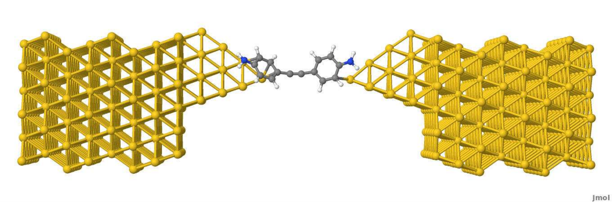
The single-molecule junction that we discuss here is shown in Fig. (49) and consists of gold (111) electrodes. The electrodes in the simulation are terminated by pyramids and bridged by a bipyridine molecule. To simulate a stretching process we have created one hundred geometries of the junction, each with a different distance between the center of the end atoms of the two leads. To optimize the atomic arrangement of each of the hundred geometries, we start from an idealized setup consisting of the two pyramids surrounded by vacuum (e.g.: not attached to the gold leads). We place the molecule slightly shifted to one side to break the symmetry and keep an Au-N bond-length of about 2 Å. We then relax the inter-atomic forces with the SIESTA code using a GGA functional[76] and a double-zeta-polarized basis set until each individual force is smaller than 0.02 eV/Å. We keep fixed the atomic positions of the bottom two layers of the pyramids during this geometry optimization. Fig. (50) shows four of the hundred relaxed configurations achieved.

We then reattach the crystalline gold leads, and impose periodic boundary conditions along the plane perpendicular to the transport direction. We use a SZ basis for the gold atoms of the leads, together with a simplified pseudo-potential, where only the 6s channel is included to speed up the simulations. However, we use a double-zeta-polarized basis set for the atoms at the gold pyramids and in the molecule. SIESTA then creates the Hamiltonian of each of the hundred junctions that we feed into GOLLUM.
Figure (51) shows the low-voltage conductance versus the electrode separation . This ’pulling curve’ shows that during the pulling process the conductance possesses a plateau, in agreement with many experiments using MCBJs. This simulation also reveals that the aromatic rings contact directly the gold surface, therefore increasing the molecule-gold coupling and the molecular conductance.

III.16 Quantum Pumping in Carbon Nanotube Archimedes Screws
So far, all calculated quantities have been obtained from the modulus squared of the scattering matrix elements. To demonstrate that GOLLUM also provides information about transport properties associated with the phases of the scattering matrix, we now examine an example of a quantum pump. Quantum pumps are time-dependent electron scatterers, which are able to transport electrons between two external reservoirs subjected to the same chemical potential. The pump process is adiabatic if the frequency of the pump cycle is smaller than the inverse of the characteristic timescale of the scatterer, the Wigner delay time[103]. Experimental [104, 105] and theoretical [106, 107, 108] studies of adiabatic quantum pumps have examined the conditions for optimal pumping and the effects of noise and dissipation.
Adiabatic pumping can be understood in terms of the parametric derivative of the full scattering matrix at fixed chemical potential [109, 110]. An adiabatically-slowly time-varying scatterer connected by ideal channels to external reservoirs, produces a current
| (100) |
pumped into the th channel, where is the energy shift matrix defined by
| (101) |
with being the full scattering matrix and the Fermi energy. Pumping can occur if the -matrix depends on time through a parameter . Hence currents can be expressed in terms of parametric derivatives
| (102) |
where is the parametric current entering channel .
Since GOLLUM gives us access to the full scattering matrix , it offers the possibility of investigating adiabatic pumping in nanostructures. We demonstrate this capability by calculating the charge pumped in a double-walled carbon nanotube nano-electromechanical device shown in Fig. (52) [111], that mimics the experimental setup of Ref. (112). Since an electron current travelling along the inner tube can cause a chiral outer tube to rotate [113], the quantum pump shown in Fig. (52) represents the inverse effect, in which rotation of the outer tube causes a current to flow along the inner tube. The position and orientation of the inner tube is kept fixed, while the shorter outer tube rotates slowly. The angle describes the real space rotation angle of the outer tube and also plays the role of the pumping parameter in this system.

To reveal the rich behavior of this family of quantum pumps, Fig. (53) shows the parametric current, as a function of the rotational angle for a typical device. Depending on the particular angle, charge may be pumped either from left to right or vice versa. The integral of this parametric emissivity within a full parametric cycle of is the number of electrons pumped per cycle.

In Fig. (54) we show the charge pumped in a (5,5) carbon nanotube with a (14,6) outer nanotube rotating slowly about it. The average pumped charge clearly drops by several orders of magnitude as the Fermi energy is increased from zero. Therefore for a most efficient pumping, the Fermi energy should be close to the Dirac point. Note however, that the pumped charge could again increase if the Fermi level is large enough to open another channel. Beyond this average behavior, there exist numerous sharp peaks in the pumped charge. The location of these peaks correlates with Fabry-Perot resonances in the reflection coefficient. This suggests that the largest pumping occurs at those resonances. In other words, when the transmission is high, pumping is low, and vice versa.

III.17 Transport in disordered systems: ballistic, diffusive and localized behavior
Finally, to demonstrate that GOLLUM can handle the disordered systems, we calculate the ensemble-averaged conductivity of a two-terminal system on a square lattice, with leads attached to a disordered scattering region as shown in Fig. (55). The width of the system is unit cells and the length is varied between to unit cells. The conductivity is defined as , where is the transmission from the left lead to right lead evaluated at the Fermi energy, eV. The tight-binding Hamiltonian of the system has a single orbital per site, with nearest neighbour couplings. eV. The site energies within the leads are eV, while the random site energies within the scattering region are uniformly distributed over the interval eV.

Figure (56) shows the the ensemble-averaged conductivity () and transmission coefficient () for the system shown in Fig. (55). It contains three regions. Within the ballistic regime between and approximately , the conductivity increases linearly with length. In the diffusive region (), the conductivity exhibits ohmic behavior and is almost independent of length. Finally for greater than 100, there is a cross over to the Anderson localized regime.

III.18 Impact of the spin-orbit interaction in the transport properties of nickel chains
We end this article by showing how the spin-orbit interaction induces gaps at certain band crossings in the one-dimensional electronic structure of infinite nickel chains. These gaps may appear or not depending on the orientation of the atomic spins relative to the axis of the chain. They lead to dips in the transmission coefficient of the chain at the gap energies.
We have simulated linear nickel chains using the DFT program SIESTA. The chains have a single atom per unit cell and are oriented along the z-axis. We have used a standard set of pseudopotential parameters, a double-zeta basis set and simple LDA for the exchange-correlation potential.
We have checked that the electronic structure and are the same for any spin orientation if the spin-orbit interaction is set to zero, as is should due rotational invariance. However, if the spin-orbit interaction is switched on, then a finite yet small magnetic anisotropy barrier appears. We have found that if we choose the atomic spins to lie along the chain axis, then there are no spin-orbit gaps close to the Fermi energy. As a consequence, the transmission coefficients with and without the spin-orbit interaction are indistinguishable from each other (as shown in Fig. (57)). In contrast, when the atomic spins are oriented in a plane perpendicular to the chain axis, then several small gaps open around the Fermi energy. These gaps are seen as dips in Fig. (57).
IV Conclusion
We have developed a new quantum transport code, which is fast, easy to use and versatile. This flexibility has been demonstrated by presenting a wide range of example calculations, encompassing charge, spin and thermal transport, corrections to density functional theory such as LDA+U and spectral adjustments, transport in the presence of non-collinear magnetism, the quantum-Hall effect, Kondo and Coulomb blockade effects, finite-voltage transport, multi-terminal transport, quantum pumps, superconducting nanostructures, environmental effects and pulling curves and conductance histograms for mechanically-controlled-break-junction experiments. Further developments are in the pipeline, including the incorporation of phonon transport. GOLLUM will soon be freely available from the following web site http://www.physics.lancs.ac.uk/gollum and the authors of this article are available to help potential users access the code.
The research presented here was funded by the Spanish Ministerio de Economía y Competitividad through the grant FIS2012-34858, by the UK EPSRC and by the European Commission FP7 ITN ”MOLESCO” Project No. 606728 VMGS thanks the Spanish Ministerio de Economía y Competitividad for a Ramón y Cajal fellowship (RYC-2010-06053). LO has been supported by the Hungarian Scientific Research Fund No. K108676. JF wishes to thank useful discussions with N. Lorente and A. Kormanyos.
Appendix A Procedures used to regularize
We have described in section II.A.2 the method employed by GOLLUM to find the surface Green’s function of each lead. However, the solution of Eq. (21) gives with some frequency numerical inaccuracies which render the method useless as it stands. These inaccuracies are caused by the highly non-singular behavior of the Hamiltonian matrix connecting adjacent PLs. We discuss here the adaptation of the method described in Refs. (9, 37) that GOLLUM uses to regularize . Mathematically, we perform an SVD decomposition of this matrix,
| (103) |
where and are unitary matrix and is a diagonal matrix containing the eigenvalues of . Numerical algorithms usually arrange them in descending order. The condition number of is defined as the ratio between the maximum and minimum eigenvalues of . determines how singular is and therefore the propensity to suffer inaccuracies when handling . Small eigenvalues appear whenever is very sparse. Physically, this is originated for example if the PL are very long so that a large fraction of hopping integrals (matrix elements of ) is zero. Our first procedure to regularize consists in adding a real or complex random matrix to . We have found that this is frequently enough to render a regular matrix. If this first procedure fails this is because the orbitals involved do not play a role in the transport properties of the lead and should be decimated out, so that the dimensions of the matrix are reduced.
Notice that reducing the dimensions of has the advantage that the computation of the surface Green’s function is much lighter. However, the procedure must be performed with some care as finally must connect with the corresponding TPL of the EM branch, whose matrices have dimensions . Explicitly, we write the Schroedinger equation of the infinite chain of the corresponding Lead:
| (104) |
where , labels the PL and runs from to and we assume that the chain will be chopped off at the PL and then connected to the TPL of the EM. We first perform the SVD decomposition of described in Eq. (103). We then set to zero all eigenvalues smaller than a given tolerance . We have checked that setting provides unproblematic and . Let us assume that we set to zero eigenvalues of , so that remain non-zero. We now construct the matrices
We transform Eq. (104) for all sites up to site as follows:
| (122) |
while the equation for sites and will be
| (123) |
We now decimate out up to site , arriving to the new set of equations
| (124) |
This set of equations generates the new Hamiltonians of each lead, and connects it with the extended molecule. Overlap matrices must also be decimated as they enter into the expression for the group velocity, Eq. (23). The denominator in this equation looks like
| (125) |
where we have applied the SVD transformation to the overlap matrices
By decimating out the unwanted degrees of freedom , we arrive at the following expressions
| (132) |
References
- [1] J. R. Heath, Molecular Electronics, Annu. Rev. Matter. Res. 39, 1 (2009).
- [2] R. L. McCreery and A. J. Bergren, Adv. Mater. 21, 4303 (2009).
- [3] K. Moth-Poulsen and T. Bjornholm, Nature Nanotech. 4, 551 (2009).
- [4] J. C. Cuevas and E. Scheer, Molecular Electronics: An Introduction to Theory and Experiment (World Scientific, Singapore, 2010)
- [5] S. Datta, Electronic Transport in Mesoscopic Systems, Cambridge University Press, Cambridge, 2007).
- [6] S. Sanvito, C.J. Lambert , J.H. Jefferson and A.M Bratkovsky, Phys. Rev. B 59, 11936 (1999).
- [7] C. W. Groth, M. Wimmer, A. R. Akhmerov, X. Waintal, Kwant: a software package for quantum transport, arXiv:1309.2926.
- [8] A. Reily Rocha, V.M. García-Suárez, S.W. Bailey, C.J. Lambert, J.Ferrer and S. Sanvito, Nature Materials 4, 335 (2005)
- [9] A. R. Rocha, V. M. García-Suárez, S. Bailey, C. Lambert, J. Ferrer and S. Sanvito, Phys. Rev. B 73, 085414 (2006).
- [10] J. Ferrer and V. M. García-Suárez, J. Mat. Chem. 19, 1696 (2009).
- [11] J. Ferrer, A. Martín-Rodero and F. Flores, Phys. Rev. B 38, 10113 (1988).
- [12] J. Taylor, H. Guo, and J. Wang, Phys. Rev. B 63, 245407 (2001).
- [13] Y. Xue, S. Datta and M. A. Ratner, Chem. Phys. 281, 151 (2002).
- [14] P. S. Damle, W. Ghosh and S. Datta, Chem. Phys. 281, 171 (2002).
- [15] M. Brandbyge, J.-L. Mozos, P. Ordejón, J. Taylor, and K. Stokbro, Phys. Rev. B 65, 165401 (2002).
- [16] J. J. Palacios, A. J. Pérez-Jiménez, E. Louis, E. San Fabián, and J. A. Vergés, Phys. Rev. B 66, 035322 (2002).
- [17] A. Pecchia and A. Di Carlo, Rep. Prog. Phys. 67, 1497 (2004).
- [18] A. Calzolari, N. Marzari, I. Souza and M. B Nardelli, Phys. Rev. B 69, 035108 (2004).
- [19] A. Arnold, F. Weigend and F. Evers, J. Chem. Phys. 126, 174101 (2007).
- [20] S. Wohlthat, F. Pauly, J. K. Viljas, J. C. Cuevas, and G. Schön Phys. Rev. B 76, 075413 (2007).
- [21] P. Darancet, A. Ferretti, D. Mayou, and V. Olevano, Phys. Rev. B 75, 075102 (2007).
- [22] D. Wortmann, H. Ishida, and S. Blügel, Phys. Rev. B 66, 075113 (2002)
- [23] J. Enkovaara et al., J. Phys.: Condens. Matt. 22, 253202 (2010).
- [24] K. Xia, M. Zwierzycki, M. Talanana, P. J. Kelly and G. E. W. Bauer, Phys. Rev. B 73, 064420 (2006).
- [25] P. Hohenberg and W. Kohn, Phys. Rev. 136, B864 (1964);
- [26] W. Kohn and L. J. Sham, Phys. Rev. 140, A1133 (1965).
- [27] J. M. Soler, E. Artacho, J.D. Gale, A. García, J. Junquera, P. Ordejón, and D. Sánchez-Portal, J. Phys.: Condens. Matter 14, 2745 (2002)
- [28] V. M. García-Suárez, C. M. Newman, C. J. Lambert, J. M. Pruneda and J. Ferrer, J. Phys.: Condens. Matt. 16, 5453 (2004).
- [29] L. Fernández-Seivane, M. A. Oliveira, S. Sanvito and J. Ferrer, J. Phys: Condens. Matt. 18, 7999 (2006).
- [30] L. Fernandez-Seivane and J. Ferrer, Phys. Rev. Lett. 99, 183401 (2007).
- [31] V. García-Suárez, D. Manrique, C. Lambert and J. Ferrer, Phys. Rev. B 79, 060408 (2009).
- [32] S. Barraza-López, K. Park, V. García-Suárez and J. Ferrer, Phys. Rev. Lett. 102, 246801 (2009).
- [33] J. P. Lewis, P. Jelınek, J. Ortega, A. A. Demkov, D. G. Trabada, B. Haycock, H. Wang, G. Adams, J. K. Tomfohr, E. Abad, H. Wang and D. A. Drabold, Phys. Stat. Solidi B 248, 1989 (2011).
- [34] C. X. Liu, X. L. Qi, H. Zhang, X. Dai, Z. Fang and S. C. Zhang, Phys. Rev. B 82, 045122 (2010).
- [35] S. Mao, A. Yamakage and Y. Kuramoto, Phys. Rev. B 84, 115413 (2011).
- [36] P. Rivero, V. Garcia-Suarez, Y. Yang, L. Bellaiche, K. Park, J. Ferrer and S. Barraza-Lopez, submitted to J. Phys.: Condens. Matter.
- [37] I. Rungger and S. Sanvito, Phys. Rev. B 78, 035407 (2008).
- [38] V. M. García-Suárez and J. Ferrer, Phys. Rev. B 86, 125446 (2012).
- [39] C. M. Finch, V. M. García-Suárez, and C. J. Lambert, Phys. Rev. B 79, 033405 (2009).
- [40] J. B. Neaton, M. S. Hybertsen and S. G. Louie, Phys. ReV. Lett. 97, 216405 (2006).
- [41] S. Y. Quek, M. Kamenetska, M. L. Stegerwald, H. J. Choi, S. G. Louie, M. S. Hybertsen, J. B. Neaton and L. Venkataraman Nat. Nanotechnol. 4, 230 (2009).
- [42] D. J. Mowbray, G. Jones and K. S. Thygesen J. Chem. Phys. 128, 111103 (2008).
- [43] A. Cehovin, H. Mera, J. H. Jensen, K. Stokbro and T. B. Pedersen, Phys. Rev. B 77, 195432 (2008).
- [44] V. M. García-Suárez and C. J. Lambert, New J. Phys. 13, 053026 (2011).
- [45] D. Goldhaber-Gordon, et al. Nature 391, 156 (1998); D. Goldhaber-Gordon et al., Phys. Rev. Lett. 81, 5225 (1998).
- [46] A. M. Uimonen,E. Khosravi, A. Stan, G. Stefanucci, S. Kurth, R. van Leeuwen and E. K. U. Gross, Phys. Rev. B 84, 115103 (2011).
- [47] Z. Liu, J. P. Bergfield, K. Burke and C. A. Stafford, arXiv:1201.131.
- [48] D. Jacob, K. Haule and G. Kotliar, Phys. Rev. B 82, 195115 (2010).
- [49] R. Korytár and N. Lorente, J. Phys.: Condens. Matter 23, 355009 (2011).
- [50] V. I. Anisimov, I. V. Solovyev, M. A. Korotin, M. T. Czyzyk and G. A. Sawatzky, Phys. Rev. B 48, 16929 (1993).
- [51] A. G. Pethukov, I. I. Mazin, L. Chioncel and A. I. Lichtenstein, Phys. Rev. B 67, 153106 (2003).
- [52] R. Bulla, T. A. Costi and T. Pruschke, Rev. Mod. Phys. 80, 395 (2008).
- [53] K. Haule, S. Kirchner, J. Kroha and P. Wolfle, Phys. Rev. B 64, 155111 (2001).
- [54] K. Haule, C.-H. Yee and K. Kim, Phys. Rev. B 81, 195107 (2010).
- [55] A. Levy Yeyati, F. Flores and A. Martín-Rodero, Phys. Rev. Lett. 83, 600 (1999).
- [56] G. Kotliar, S. Y. Savrasov, K. Haule, V. S. Oudovenko, O. Parcollet and C. A. Marianetti, Rev. Mod. Phys. 78, 866 (2006).
- [57] J. Ferrer, A. Martin-Rodero and F. Flores, Phys. Rev. B 36, 6149 (1987).
- [58] D. R. Hofstadter, Phys. Rev. B 14, 2239 (1976).
- [59] Lambert C.J., J. Phys.: Condens. Matter, 3 6579 (1991)
- [60] Hui V.C. and Lambert C.J., J. Phys.: Condens. Matter 2 7303 (1990)
- [61] C. J. Lambert, and R. Raimondi, Journal of Physics: Condensed Matter 10(5), 901 (1998).
- [62] N.K. Allsopp, V.C. Hui, C.J. Lambert and S.J. Robinson, J. Phys.: Condens. Matter 6 10475 (1994)
- [63] N.R. Claughton, and C.J. Lambert, Phys. Rev B 53, 1 (1996)
- [64] T.T. Heikkila, M.P. Stenburg, M.M. Salomaa and C.J. Lambert, Physica B 284, 1862 (2000)
- [65] F. Taddei, S. Sanvito, C.J. Lambert and J.H. Jefferson, Phys. Rev. Lett. 82, 4938 (1999)
- [66] V.F. Falko, A.F. Volkov and C.J. Lambert, Phys. Rev. B 60 15394 (1999)
- [67] E. McCann, V.I. Fal’ko, A.F. Volkov and C.J. Lambert, Phys. Rev. B 62, 6015 (2000)
- [68] P. Makk, D. Visontai, L. Oroszl´any, D. Zs. Manrique, Sz. Csonka, J. Cserti, C. J. Lambert, A. Halbritter, Phys. Rev. Lett. 107 276801 (2011)
- [69] C.J. Lambert, J. Phys.: Condens. Matter 5 707 (1993)
- [70] V.C. Hui and C.J. Lambert, Euro. Phys. Lett, 23 203 (1993)
- [71] A. Volkov, N. Allsopp and C.J. Lambert, J.Phys.: Condens. Matter L45 (1996)
- [72] V. M. García-Suárez, A. R. Rocha, S. W. Bailey, C. J. Lambert, S. Sanvito, J. Ferrer, Phys. Rev. 72, 045437 (2005).
- [73] D. Jacob, J. Fernández-Rossier, and J. J. Palacios, Phys. Rev. B 71, 220403(R) (2004).
- [74] D. Jacob, J. Fernández-Rossier, and J. J. Palacios, Phys. Rev. B 77, 165412 (2008).
- [75] M. Häfner, J. K. Viljas, and J. C. Cuevas, Phys. Rev. B 79, 140410(R) (2009).
- [76] J. P. Perdew, K. Burke, and M. Ernzerhof, Phys. Rev. Lett. 77, 3865 (1996).
- [77] M. Dion, H. Rydberg, E. Schröder, D. C. Langreth, and B. I. Lundqvist, Phys. Rev. Lett. 92, 246401 (2004).
- [78] G. Román-Pérez and J. M. Soler, Phys. Rev. Lett. 103, 096102 (2009).
- [79] V. M. García-Suárez, R. Ferradás, D. Carrascal and J. Ferrer, Phys. Rev. B 87, 235425 (2013).
- [80] V. I. Anisimov, J. Zaanen, O. K. Andersen, Phys. Rev. B 44, 943 (1991).
- [81] S. L. Dudarev, G. A. Botton, S. Y. Savrasov, C. J. Humphreys and A. P. Sutton, Phys. Rev. B 57 1505 (1998).
- [82] R. Ferradás, V. M. García-Suárez and J. Ferrer, J. Physics: Condens. Matt. 25, 325501 (2013).
- [83] V. Kaliginedi, P. Moreno-Garcìa, H. Valkenier, W. Hong, V. M. García-Suàrez, P. Buiter, J. L. H. Otten, J. C. Hummelen, C. J. Lambert and T. Wandlowski, J. Am. Chem. Soc. 134, 5262 (2012).
- [84] J. P. Perdew and A. Zunger, Phys. Rev. B 23, 5075 (1981).
- [85] J. Ferrer and V. M. García-Suárez, Phys. Rev. B 80, 085426 (2009).
- [86] A. M. Bratkovsky and P. E. Kornilovitch, Phys. Rev. B 67, 115307 (2003).
- [87] C. Evangeli, K Gillemot, E. Leary, M. T. Gonzalez, G. Rubio-Bollinger, C. Lambert and N. Agrait, Nano letters 13, 2141 (2013).
- [88] L. Wang and H. Cheng, Phys. Rev. B 69, 165417 (2004).
- [89] X. Zheng, Z. Dai, Z. Zeng, J. Phys. Condens Matter. 21, 145502 (2009).
- [90] T. Bohler, A. Edtbauer, E. Scheer, Phys. Rev. B. 76, 125432 (2007).
- [91] M. Kiguchi, K. Murakoshi, J. Phys. Chem. C 112, 8141 (2008).
- [92] N. Neel, J. Kroger, L. Limot, T. Frederiksen, M. Brandbyge, R. Berndt, Phys. Rev. Lett. 98, 065502 (2007).
- [93] L. Algharagholy, S. W. D. Bailey, T. Pope and C. J. Lambert, Phys. Rev. B 86, 075427 (2012).
- [94] E. Leary, H.Höbenreich, S. J. Higgins, H. van Zalinge, W. Haiss, R.J. Nichols, C. Finch, I. Grace and C.J. Lambert, Phys Rev. Lett. 102, 086801 (2009)
- [95] S. Plimpton, J. Comp. Phys. 117, 1 (1995); http://lammps.sandia.gov.
- [96] I.T. Todorov, W. Smith, K. Trachenko and M.T. Dove, J. Mat. Chem. 16, 1911 (2006).
- [97] J. J. Kasianowicz, et al., Proc. Natl. Acad. Sci. USA 93, 13770 (1996).
- [98] J. Mathé et al., Proceedings of the National Academy of Science 102, 12377 (2005).
- [99] G. F. Schneider, Nano letters 10, 3163 (2010).
- [100] C. A. Merchant, et al., Nano letters 10, 2915 (2010).
- [101] S. Garaj, et al., Nature 467, 190 (2010).
- [102] C. Sathe, et al., ACS nano 5, 8842 (2011).
- [103] E. P. Wigner, Phys. Rev. 98, 145 (1955).
- [104] H. Pothier, P. Lafarge, C. Urbina, D. Esteve and M. H. Devoret, Europhys. Lett. 17, 249 (1992).
- [105] M. Switkes, C. M. Marcus, K. Campman and A. C. Gossard, Science 283, 1905 (1999).
- [106] F. Zhou, B. Spivak and B. Altshuler, Phys. Rev. Lett. 82, 608 (1999).
- [107] J. E. Avron, A. Elgart, G. M. Graf and L. Sadun, Phys. Rev. B 62, R10618 (2000).
- [108] J. E. Avron, A. Elgart, G. M. Graf and L. Sadun, Phys. Rev. Lett. 87, 236601 (2001).
- [109] M. Büttiker, H. Thomas and A Prêtre, Z. Phys. B: Condens. Matter 94, 133 (1994).
- [110] P. W. Brouwer, Phys. Rev. B 58, R10135 (1998).
- [111] L. Oroszlany, V. Zolyomi and C. J. Lambert, ACS Nano 4, 7363 (2010).
- [112] A. M. Fennimore, T. D. Yuzvinsky, Wei-Qiang Han, M. S. Fuhrer, J. Cumings and A. Zettl, Nature 424, 408 (2003).
- [113] S.W.D. Bailey, I. Amanatidis, and C.J. Lambert, Phys. Rev. Lett. 100 256802 (2008)