Influence of interface potential on the effective mass in Ge nanostructures
Abstract
The role of the interface potential on the effective mass of charge carriers is elucidated in this work. We develop a new theoretical formalism using a spatially dependent effective mass that is related to the magnitude of the interface potential. Using this formalism we studied Ge quantum dots (QDs) formed by plasma enhanced chemical vapour deposition (PECVD) and co-sputtering (sputter). These samples allowed us to isolate important consequences arising from differences in the interface potential. We found that for a higher interface potential, as in the case of PECVD QDs, there is a larger reduction in the effective mass, which increases the confinement energy with respect to the sputter sample. We further understood the action of O interface states by comparing our results with Ge QDs grown by molecular beam epitaxy. It is found that the O states can suppress the influence of the interface potential. From our theoretical formalism we determine the length scale over which the interface potential influences the effective mass.
pacs
73.21.La, 78.67.Hc, 68.65.-k, 73.90.+fI Introduction
Si and Ge nanostructures (NSs) remain amongst the most important materials for photovoltaic and electronic applications [1, 2]. Si is extensively used in the microelectronics industry partly due to the importance and stability of its oxide [3]. The Ge oxide states can create complications in NSs. Fabrication of Ge NSs in a SiO2 matrix often results in a high concentration of interface defect states [4, 5, 6], because Ge can easily occupy the Si position within the SiO2 matrix due to its low formation energy. Sub-oxide interface states give rise to a defect photoluminescence (PL) band that can dominate quantum confinement (QC) effects [5]. However, with careful control over the fabrication [7] and characterization [8] conditions, Ge NSs do clearly demonstrate QC effects. Furthermore, because of a larger Bohr radius in Ge compared to Si, Ge has the advantage of greater tunability in the gap energy () due to QC [9]. Moreover, it was recently demonstrated that interface defect states may enhance the efficiency of photovoltaic devices due to preferential hole trapping [9].
The nature of its interfacial structure is arguably the defining parameter of a NS. Fundamentally, the introduction of an interface modifies bulk parameters [5] and introduces new phenomena. Interface states can break valley degeneracy [10]. Dangling bonds, stress, and defect states elicit the degree to which the interface potential confines charge carriers [5]. Hydrogen versus oxygen termination at the interface influences the oscillator strength [11] and creates polarization effects at the interface [12]. Nanostructure sensing devices rely on the charge configuration at the interface, which ‘communicates’ with the environment [13] and determines the conductivity within the NS [14]. Nonetheless, the role of the interface remains largely misunderstood [15]. The exact band energy alignment at the interface remains a topic of intense research [16], as it is difficult to establish the exact chemical environment at the interface [17]. Defect engineering at the interface can have a complicated effect on the QC of the charge carriers [18, 19], which can be difficult to model theoretically [20, 21].
The crystal potential changes across the interface of a NS and thus the carrier effective mass (EM) changes, which is modelled by invoking the Bastard-type boundary conditions [22, 23, 24, 25]. There is experimental [6, 26, 27, 28] and theoretical [29, 30] evidence that the EM should depend on the NS dimension. Understanding how the EM varies in low-dimension remains a challenge as experimental measurements are model dependent [31, 32] and it is difficult to theoretically scale the EM to low dimensions [6, 33]. Density functional theory (DFT) was used to calculate the EM from the density of states [29]. However, it is not clear how to model the interface nor the excited states within DFT [34, 25].
A common pitfall in theoretical modelling is the lack of information regarding the interface atomic potentials, which leads to extensive use of H-terminated surfaces at the expense of the experimental details [5]. Sub-oxide interfaces are typically modelled using OH termination [35, 36]. The local density approximation is used to correct for the local charge environment to obtain agreement with the experimental optical gap [35, 5]. However, there are recent theoretical results using embedding matrices, such as SiC [37]. Ref. 33 embedded Si NSs in a SiO2 matrix by inserting O atoms between Si-Si bonds followed by a randomizing procedure leading to defect and stress free structures. Therefore, relaxed assumptions are required to obtain agreement with experiment and the defect landscape cannot be readily included [38, 39].
Owing to the rich variety of phenomena that the interface can give rise to, understanding the contribution of the individual components can be difficult. Indeed, theoretical studies have suggested[40, 6, 5] , where and is the NS diameter, which has been demonstrated experimentally [41, 42, 5]. In this work, we elucidate the precise role of the interface potential on the EM. An analytic formalism for the EM and interface [30] was developed and applied to study Ge quantum dots (QDs) grown by molecular beam epitaxy (MBE) [43]. The parameters developed during our study on MBE Ge QDs are transferred to the present study on rf-magnetron co-sputtering (sputtering), and plasma enhanced chemical vapour deposition (PECVD) Ge QDs. The PECVD and sputter samples were chosen for this work because they were fabricated under similar experimental conditions, but exhibit a measurable variation in the chemical structure of the interface. Both sputtered and PECVD QDs have the same dimensional dependence as the MBE QDs, which allows us to isolate the role of the interface potential on the EM.
Comparing PECVD and sputter samples, it is found that as the interface potential increases the EM is reduced thus increasing the confinement energy. We determine the length scale at which the EM is modified due to the interface potential. Furthermore, by comparing with MBE Ge QDs we find that O interface states can suppress this mechanism. These results are important for solar cell applications, as we recently demonstrated that defects at the interface can be engineered to enhance the light harvesting capabilities in Ge QDs [9].
II Experiment
In this work, we focus our analysis on experimental results from two fabrication methods for Ge quantum dots (QDs) that produce different interface potentials. Thin films of Ge-rich SiO2 were deposited using either PECVD [8] or sputtering [9]. Thermal annealing was carried out at 800 oC or 600 oC in N2 for PECVD or sputtered samples, respectively, to promote Ge QD nucleation. In Refs. 8, 9, the experimental details of diameter control and determination are discussed along with crystallinity measurements. Both PECVD and sputtered QDs were determined to be in an amorphous state with a bulk gap energy () of 0.8 eV. The average diameter in the sputter samples varies from 2 to 4 nm, while in PECVD samples it varies from 3.5 to 8.4 nm. Optical absorption measurements were performed to assess the variation in with QD diameter. Ge NSs embedded in an oxide matrix typically demonstrate a PL spectrum dominated by a high concentration of sub-oxide related defects at the interface between the Ge NS and the oxide matrix, thus masking the QC related PL band [5]. In Refs. 8 and 9, the absorption spectrum was considered over the PL spectrum, because defects states in the GeO2 interface made it difficult to measure the variation of with QD diameter from the emission spectrum [44], which is more sensitive to mid-gap defects [45]. Finally, it is worth noting that due to NS size distribution and carrier leakage there is some inherent error in associating the NS experimental with the correct experimental , see Ref. 5 for more details.
From the absorption spectra, the oscillator strength, and was found in Refs. 8, 9 for each using the Tauc method. The applicability of the Tauc method to NSs is discussed in detail in Ref. 9. The Tauc method is based on a semi-empirical model for amorphous systems, which assumes parabolic band edges and optical inter-band transitions between quasi localized states (i.e. momentum is not conserved) [46]. Indeed, the method assumes that the dipole-matrix element (proportional to the oscillator strength) is not -dependent. Breaking of momentum (-vector) conservation is a fundamental tenant of quantum confinement in NSs. Furthermore, our NSs are amorphous and thus lack long range order. In addition, the parabolic band edge picture can still be applied in a NS as discussed in the next section. A deviation from linearity happens at low due to Urbach tail regions. For this reason, the estimation of for amorphous materials is usually performed for values of larger than 210-9 cm2 (for our samples) where a clear linear trend in the Tauc plots appears [47]. Furthermore, the was calculated from scanning tunnelling spectroscopy measurements on Ge QDs to be 1.4 eV [48]. This value agrees with our determined via the Tauc method for a similar diameter range. Therefore, we find that the Tauc method works well for amorphous NSs and has been experimentally demonstrated in the literature [47, 27].
III Theory
The analysis of the experimental data is carried out using a variety of theoretical tools. The approach taken in this work considers an interface-related correction to the EMA. The validity of the EMA has been widely debated in the literature [5]. Generally, it is assumed that the parabolic band approximation breaks down at low-dimension and thus the EMA cannot be applied. However, recently it has been shown that a notion of a ‘fuzzy-band-structure’ holds for NSs down to 2 nm [49], and that the method does produce the correct symmetry of a QD [50]. The EMA is a first order approximation of the generalization that considers transitions only at the conduction band minimum (CBM) and valence band maximum (VBM). In a NS, transitions mainly occur near the Brillouin zone center (the -point), due to breaking of the momentum selection rules [6]. This type of transition is referred to as pseudodirect [51, 52]. From a theoretical perspective, pseudodirect behavior allows one to ignore phonon events in the formalism. When a 30-band model is considered, spurious solutions are found, which can be removed computationally [53]. A two-conduction-band approach has also been used [54] to describe conduction band hybridization, and a two-band approximation [6] demonstrates good agreement with experiment [25]. A justification of the EMA is given in detail in Refs. 6, 5. DFT models including interface corrections have been employed in the literature [36, 21], and produce a similar dimensional dependence as the method presented here [35]. However, we opt for the present approach because of the clarity in the physics at the interface. Also, the DFT approaches use a different interface passivation from the actual experiment one.
First, we employ a new theoretical formalism using a spatially dependent effective mass (SPDEM), as detailed in Ref. 30 and formulated in Refs. 55, 56. The important feature here is the introduction of an inverse characteristic length scale: , where is the QD diameter in nanometres. is not tunable, but was derived in Ref. 30 and modifies the dispersion relation of the charge carriers as described in Sec. V. acts as a coupling parameter between the momentum of the charge carriers and the confinement potential. In this formalism, the confinement potential, , was given by:
| (1) |
where is the particle position in the direction, and is defined as the energy difference between the QD and the matrix material at the CBM or the VBM for an electron () or hole (), respectively. Using a point canonical transformation (PCT), we demonstrated that the SPDEM is directly related to the confinement potential. This effect is analogous to the relationship between the crystal potential and the bare electron mass [30]. Therefore, the SPDEM formalism is well adapted to describe the effect of on the effective mass and yields the dispersion relation:
| (2) |
where , and are the bulk electron and hole effective mass, respectively.
The second model used in our analysis is the effective mass approximation (EMA), as detailed in Ref. 6. This model describes electron-hole confinement conditions within an infinite confinement potential context, according to the relation:
| (3) |
We note that EMA presented here is used to describe only the effect of reduced dimension on the electron and hole and includes no additional effects. However, we discovered a physically significant phenomenological correction [43] to both the SPDEM and EMA models, which was applied to obtain agreement between the two theories, given by:
| (4) | |||
| (5) |
where a=0.047 nm-2, b=0.160 nm-1, and c=-0.035 are identical for both renormalized masses, and , and were determined in Ref. 43. The parameters ‘a’, ‘b’, and ‘c’ were determined from PL measurements on MBE Ge QDs [43]. Ref. 57 noted that these QDs experience strong exciton localization and thus there is no Stokes shift between the absorption and emission spectrum. According to the theory of QC, localization in position space breaks the momentum selection rules and thus phonon coupling is not required for indirect gap materials [5]. In Refs. 5, 6 we noted that a measured Stokes shift was a consequence of interfacial phononic modes (e.g. vibrons). Strong breaking of the momentum selection rules (or time-reversibility) denoted as ‘strong confinement’ is included in both the EMA [6] and SPDEM [30] models. We showed previously [6] that amorphous NSs experience strong confinement in the electron and hole states.
In our model, the interface potential influences the effective mass, as noted above and discussed in Sec. V. The parameters in and renormalize the bulk reduced mass, , and will be discussed in Sec. IV. Therefore, we conclude that the parameters ‘a’, ‘b’, and ‘c’ are valid for both absorption and emission spectrum, while the influence of the interface is contained in the parameter ‘e’.
The parameters ‘a’, ‘b’, and ‘c’ are the same for all Ge QD samples and their physical significance is discussed further in Sec. V. Our aim in this work is to understand the influence of the interface on the EM. This influence is contained solely in the parameter ‘e’, which is introduced as correction to the EMA and SPDEM models. This parameter gives us access to the macroscopic features of the interface that would otherwise be inaccessible within the standard EMA. Therefore, when we use Eqs. (4) and (5) with Eqs. (2) and (3), respectively, we obtain perfect agreement in the dispersion relations [43] allowing us to isolate essential differences in the physics between the two models, as described Sec. V. It is important to note that we are presenting a phenomenological analysis and not presenting these models as an alternative to previously existing theoretical models. Our intention is to compare the results of two models across different fabrication methods to extract physically relevant information correlated with the variation in our parameter set.
III.1 Methodology
For the sputter and PECVD Ge QDs, we use Eqs. (4) and (5) in the SPDEM- and EMA- (see Ref. 43) models to determine the relationship between the interface potential and EM. For all QD samples the term in Eqs. (4) and (5) is the same, thus ensuring that all samples have the same dimensional dependence as found in Ref. 43. Therefore, we are left to determine only , , and the parameter .
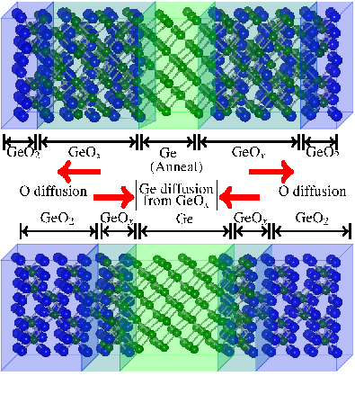
First, we consider and . From x-ray photoemission spectroscopy (XPS) in sputtered Ge QDs, a Ge-Ge signal was measured in the as-deposited film, see Fig. 1. This signal indicated that Ge QDs formed upon initial film deposition. From the XPS results, no Ge-Si nor Si-Si signal are observed indicating that all of the Ge is either within the QD or in an oxide state, and all of the Si is in the SiO2 state [9]. Therefore, sputter thin film deposition, under our given experimental conditions, can be modelled approximately by the random mixture model (RMM) [58, 44]. This model supposes that the film is described by the formation of a mixture of Ge, GeOx, and GeO2 centres [59]. A representation of the RMM is given in Fig. 2. In the top part of Fig. 2, we indicate a region of Ge surrounded by layer of GeOx and a thin layer of GeO2. Upon annealing, the Ge QD diameter and the stoichiometric oxide concentration increase. This is a result of Ge diffusing from the Ge-rich GeOx region into the Ge QD region [60], which is indicated in the bottom part of Fig. 2. Simultaneously, it is possible that O diffuses toward the GeO2 region. This observation implies that the interface between the Ge QD and the matrix material is comprised of a large concentration of GeOx states. As a first approximation, we consider a Ge-GeO interface with a potential of approximately = 0.6 eV and = 1.8 eV [61].

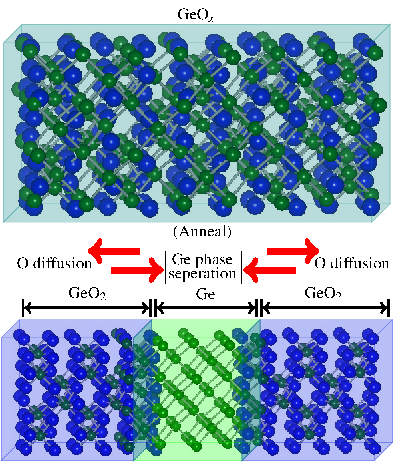
In the case of PECVD QDs, a different behaviour was observed. Here the QDs are more accurately modelled by the random bonding model (RBM), under our given experimental conditions [58], see Fig. 3. In the RBM all of the Ge is assumed to be in one of its oxide states [63]. Raman measurements (see Ref. 8) indicate that upon deposition the film is primarily in a Ge sub-oxide state, i.e. there is no clear observation of a Ge-Ge signal, as represented in the top part of Fig. 3. After annealing, GeOx will phase separate into Ge QDs and GeO2 mediated by Ge diffusion, as represented in the bottom part of Fig. 3. As in the case of sputter QDs, it is possible that O undergoes diffusion as well. This behaviour implies that the interface is mainly composed of GeO2. Though there must still exist a small concentration (as compared to sputtered Ge QDs) of GeOx right at the interface, which will lower the interface potential slightly from the ideal GeO2 value. Therefore, we assume that the interface potential is close to the value of Ge-GeO2, which is = 1.2 eV and = 3.6 eV [64].
The final step is to determine for both the SPDEM and EMA models. We consider a Tauc plot of the experimental absorption cross section, , for PECVD and sputtered Ge QDs from Refs. 8 and 9, respectively. is modelled via the relation:
| (6) |
where is proportional to the the oscillator strength and was determined experimentally, and is the photon energy. is given by either SPDEM- or EMA-, in Eq. (6). and was determined experimentally in Refs. 8 and 9, see Sec. II. In the case of EMA-, we fit Eq. (6) via to the experimental data for each QD and . For SPDEM-, as we noted above, the interface potential was approximated from our discussion of the RMM, or RBM for the sputter, or PECVD samples, respectively. Since these models are only a first approximation we allowed and to vary within 25 of their proposed values, and then we fitted Eq. (6) to the data by varying and for each experimental QD and .
IV Results
The results obtained from fitting SPDEM- to the sputtered and PECVD samples are shown in Figs. 4 and 5, respectively. The deviation from linearity in the experimental data at low is due to Urbach tail regions, i.e. defect states near the band edge, which are common to amorphous structures as in this work [9]. In PECVD samples (Fig. 5) there is a deviation from linearity at high due to a partial crystalline transition in less than 30 of the QDs after annealing at 800 oC [8]. When the fit was constrained to the linear region, a less than 1 difference was found in our final fitting parameters compared to fitting over the entire data set. The fitted value for is listed for each QD in Figs. 4 and 5, and the resultant interface potential (also shown), was found to be notably identical (within 1) for each QD . for each QD are the same within experimental error, therefore, in our formulation of we use the average value, =0.181, and 0.090 for sputter, and PECVD, respectively. Likewise, varies only within experimental error. The results of our analysis are summarized in Table 1. Table 1 also lists the results from the EMA fit and the values for MBE Ge QDs.


| Sputter | |||||
| 2 nm | 2.5 nm | 3 nm | 4 nm | ||
| 0.528 | 0.597 | 0.583 | 0.499 | 0.552 | |
| (nm-1) | 0.173 | 0.195 | 0.191 | 0.163 | 0.181 |
| =0.92 eV =2.80 eV | |||||
| PECVD | |||||
| 3.5 nm | 4.4 nm | 8.4 nm | |||
| 0.203 | 0.268 | 0.288 | 0.253 | ||
| (nm-1) | 0.072 | 0.095 | 0.102 | 0.090 | |
| =1.09 eV =3.28 eV | |||||
| MBE | |||||
| 0.378 | |||||
| (nm-1) | 0.059 | ||||
| =0.20 eV =0.66 eV | |||||
In Fig. 6, we plot the experimental data for PECVD [8] and sputter [9] Ge QDs along with the SPDEM- curve. The interface potential, , and are listed in Fig. 6 for reference. In Sec. III, we mentioned that the SPDEM- and EMA- models agree with each other. The parameters , , and in Eqs. (4) and (5) were found by analysing MBE grown Ge QDs [43]. There is good agreement between the experimental data and our calculation, noting that the error bars in the of the PECVD samples are on the order of 2 nm [8].

The for the PECVD grown samples is higher than the sputter samples. The reason for the difference is understood within our models. From the SPDEM- model, we find a larger interface potential in PECVD samples compared to the sputter samples. The larger interface potential is correlated with a larger reduction in , which increases the confinement energy. MBE Ge QDs were fabricated with an a-Si matrix, which has a lower interface potential than both PECVD and sputter Ge QDs, see Fig. 6. However, the is comparable to the other two samples with a value of in between the PECVD and sputter values. It is difficult to make a full comparison between the sputter and PECVD samples versus the MBE samples, because the MBE samples were fabricated under very different conditions. However, we can consider a few essential differences. In the case of the MBE QDs there are no O-defect states [65, 43], because of the unique fabrication method. O-defect states at the interface increase the spread of the wave-function, thus lowering the confinement energy [12]. Furthermore, O interface states can pin the charge carriers, again lowering the confinement energy [6, 5]. The combination of these phenomena lowers the confinement energy in PECVD and sputter samples, in agreement with theoretical predictions [12], and it becomes comparable to that in MBE samples (see Fig. 6). Therefore, we understand that the O interface states are the source of the difference between the sputter and PECVD samples versus the MBE samples. Nonetheless, we see that for a higher interface energy a larger reduction in the EM is obtained.
V Discussion
A closer examination of the results shown in Table 1 in the context of our models allows us to understand the nature of the confinement mechanism. As mentioned in Sec. III, the SPDEM theory models a modification in the EM due to the interface potential. In Ref. 30, we derive the envelope function within the SPDEM formalism:
| (7) |
where is the Gaussian strength. In Fig. 7, we plot the probability amplitude of Eq. (7) for a 6 nm QD as a function of the interface potential and particle position. As the interface potential increases, the probability amplitude is increasingly localized, which implies increasing de-localization in momentum space. A Fourier transformation of Eq. (7) demonstrated that the SPDEM envelope function exhibits an increased spread in momentum space compared to a Gaussian envelope function [30]. The interface potential alters the SPDEM envelope function because of the introduction of , which modified the EM through the relation [30]:
| (8) |

Therefore, from we can find the length scale at which the EM begins to change, which is 16.95, 11.11, and 5.53 nm in MBE, PECVD, and sputter samples, respectively. At the stated dimensions the SPDEM energy begins to deviate from the experimental data and corrects for this behaviour. In Fig. 8 we plot and from Eqs. (4) and (5), respectively, where the role of can be seen. Below diameters of around 16 and 11 nm the MBE and PECVD curves are less than 1 indicating that increases below these dimensions. The difference between the cross-over dimension depicted in Fig. 8 and the value obtained from is because of experimental error. We note that in Fig. 8 the curve for the sputter sample does not fall below 1. In Ref. 43, we determined that above 6.2 nm the dispersion relation is dominated by the SPDEM- relation. Therefore, the sputter value of 5.53 nm indicates that the SPDEM mechanism is suppressed in these samples. The different behaviour found for the sputter samples is a consequence of their interface quality (Secs. III.1 and IV). The lower interface potential does not create a strong confinement condition for the charge carriers, see Fig. 7. Additionally, the sub-oxide interface states promote de-localization of the wave-function in real space [12].

The values obtained for also agree with the results of Fig. 6. First, we note that the value obtained for the MBE samples of 16 nm is on the order of the Bohr radius for Ge. This result is what we expect in these samples, because of the high quality interface. At 16 nm, the charge carriers in the MBE samples begin to experience the influence of the confinement potential and thus their energy is modified, as predicted by QC. While in the PECVD and sputter samples, the onset of QC is suppressed from the expected Bohr radius value. Therefore, the PECVD and sputter samples experience the effects of QC over a smaller diameter range compared to MBE, and thus their shift is not as great.
The relationship between pure QC effects and a modified EM are understood by comparing the SPDEM- results with respect to the EMA- results. In a previous work on Ge QDs buried in a-Si [43] we found that above 6.2 nm the , due to a modification in the EM, while below 4.6 nm the , due to pure QC effects. These parameters come from the term in Eqs. (4) and (5), and represent a universal dimensional dependence. The parameter represents a correction to these ideal length scales due to additional effects not included in the theory, which in our analysis include the O-interface states. If we consider the ratio , then we obtain 3.05 and 2.81 nm for sputter and PECVD samples, respectively. This length scale signifies when the confinement behaviour changes from the SPDEM to the EMA model and is depicted in Fig. 8 by the vertical line at 2.9 nm. Within experimental error, we thus find that pure QC effects dominate at 2.9 nm, which is suppressed from the ideal case (between 6.2 and 4.6 nm) due to the interface states. On the other hand, the same ratio in MBE samples gives 6.4 nm (see vertical line in Fig. 8), which is in agreement with the ideal value (6.2 nm), because there are no O interface states in this sample. Finally, this is in agreement with previous results obtained in Ref. 43, where the MBE value of 6 nm was found to be the dimension that produces the most efficient luminescence. From our work here we understand this result on the basis that this is the dimension at which the behaviour changes from SPDEM to EMA and thus carriers are strongly confined.
We illustrate collectively all of the phenomena described in this manuscript in Fig. 9. At the top of the figure we recall the dimensional dependence of the SPDEM- and EMA- models. Fig 9 is divided into two parts. In the ‘pink’ region of the figure above 6 nm, the dominant model is SPDEM-, which models a change in in conjunction with a change in the EM. The ‘grey’ region below 4 nm is modelled according to the EMA- where pure QC effects dominate. The ‘pink’ and ‘grey’ regions were determined from the results of Ref. 43 and come from the universal dimensional parameters , and in the term .

From the parameter , we determined the onset of the SPDEM behaviour at 16, 11, and 5 nm in the MBE, PECVD, and sputter samples, respectively. The change in energy due to SPDEM is represented by the solid curved line in Fig. 9 for the three samples (not drawn to scale). The MBE sample’s value is in agreement with the Bohr radius for Ge and indicates when the charge carriers first ‘feel’ the confinement potential. In the case of PECVD and sputter samples this value is suppressed due to the O states at the interface, which cause the wave-function to leak into the matrix and thus lowers the confinement energy, as described above. The PECVD case has a higher value than the sputter case due to the higher confinement potential and thus experience a larger change in , due to an increased reduction in the EM.
The transition point from SPDEM to EMA is on the order of 5 nm according to the transition from the ‘pink’ to the ‘grey’ region in Fig. 9. From the ratio of to we determined this transition for each sample. The change in energy due to EMA is represented by the dashed curved line in Fig. 9 for the three samples (not drawn to scale). In the case of MBE sample, the transition is in agreement with the calculated value at 6 nm, because of the lack of O at the interface. While in PECVD and sputter samples they both change behaviour at around 3 nm. The suppression here again is due to O interface states, as described above.
VI Conclusion
Using a previously developed theoretical formalism as an analytical tool we have been able to understand the relationship between the EM and the interface potential. We found that when the interface potential was large there exists a strong reduction in the EM. This condition was clearly demonstrated when comparing PECVD and sputter samples, where the PECVD case has a larger interface potential. However, if the sample contains O states at the interface, then the confinement energy was reduced due to these states. This result was noted by comparing MBE samples with no O interface states to the PECVD and sputter samples. We determined the length scale where the samples begin to experience a modification in due to a change in the EM, which was 16, 11, and 5 nm for MBE, PECVD, and sputter samples, respectively. The lower values in PECVD and sputter samples compared to MBE samples were understood in terms of the O interface states. We found the length scale where the QC mechanism changes from SPDEM to EMA, which was 6, and 3 nm in MBE and PECVD/sputter samples, respectively. All of these results are summarised graphically in Fig. 9. These results indicate an additional carrier confinement mechanism in NSs, which can be exploited for device fabrication through interface engineering. From this work, we have found a dynamic relationship between the magnitude of the interface potential and the EM with respect to the chemical composition of the interface.
Acknowledgements.
We would like to thank N. L. Rowell from NRC-Ottawa; I. Berbezier, G. Amiard, L. Favre, and A. Ronda from UMR CNRS-Marseille; and M. Faustini, and D. Grosso from UMR-7574 UPMC-CNRS-Paris for their valuable experimental contributions and insights with respect to MBE grown Ge QDs. R.N.C.F. acknowledges funding from CNPq (Brazilian agency). S.C., A.T., and S.M. acknowledge MIUR projects, and ENERGETIC (PON003553391233). E.G.B. and S.M. acknowledge PLASTICs (PON02003553416798).References
- [1] S. K. Ray, S. Maikap, W. Banerjee, and S. Das, J. Phys. D: Appl. Phys. 46, 153001 (2013).
- [2] L. Mangolini, J. Vac. Sci. Technol., B 31, 020801 (2013).
- [3] F. A. Zwanenburg, A. S. Dzurak, A. Morello, M. Y. Simmons, L. C. L. Hollenberg, G. Klimeck, S. Rogge, S. N. Coppersmith, and M. A. Eriksson, Rev. Mod. Phys. 85, 961 (2013).
- [4] K. S. Min, K. V. Shcheglov, C. M. Yang, H. A. Atwater, M. L. Brongersma, and A. Polman, Appl. Phys. Lett. 69, 2033 (1996).
- [5] E. G. Barbagiovanni, D. J. Lockwood, P. J. Simpson, and L. V. Goncharova, Appl. Phys. Rev. 1, 011302 (2014a).
- [6] E. G. Barbagiovanni, D. J. Lockwood, P. J. Simpson, and L. V. Goncharova, J. Appl. Phys. 111, 034307 (2012).
- [7] D. J. Lockwood, N. L. Rowell, E. G. Barbagiovanni, L. V. Goncharova, P. J. Simpson, I. Berbezier, G. Amiard, L. Favre, A. Ronda, M. Faustini, and D. Grosso, ECS Transactions 53, 185 (2013).
- [8] S. Cosentino, E. Sungur Ozen, R. Raciti, A. M. Mio, G. Nicotra, F. Simone, I. Crupi, R. Turan, A. Terrasi, A. Aydinli, and S. Mirabella, J. Appl. Phys. 115, 043103 (2014a).
- [9] S. Cosentino, E. G. Barbagiovanni, M. Miritello, G. Nicotra, I. Crupi, D. Pacifici, S. Mirabella, and A. Terrasi, Sol. Energy Mater. Sol. Cells (2014b), 10.1016/j.solmat.2014.09.012.
- [10] A. Dusko, A. L. Saraiva, and B. Koiller, Phys. Rev. B. 89, 205307 (2014).
- [11] R. Guerra and S. Ossicini, Phys. Rev. B. 81, 245307 (2010).
- [12] R. Guerra, M. Marsili, O. Pulci, and S. Ossicini, Phys. Rev. B. 84, 075342 (2011).
- [13] G. Mattioli, S. B. Dkhil, M. I. Saba, G. Malloci, C. Melis, P. Alippi, F. Filippone, P. Giannozzi, A. K. Thakur, M. Gaceur, O. Margeat, A. K. Diallo, C. Videlot-Ackermann, J. Ackermann, A. A. Bonapasta, and A. Mattoni, Adv. Energy Mater. 1301694 (2014).
- [14] S. Rühle, A. Y. Anderson, H.-N. Barad, B. Kupfer, Y. Bouhadana, E. Rosh-Hodesh, and A. Zaban, J. Phys. Chem. Lett. 3, 3755 (2012).
- [15] K. Dohnalová, T. Gregorkiewicz, and K. Kůsová, J. Phys. Condens. Matter 26, 173201 (2014).
- [16] G. Seguini, C. Castro, S. Schamm-Chardon, G. BenAssayag, P. Pellegrino, and M. Perego, Appl. Phys. Lett. 103, 023103 (2013).
- [17] K. Hirose, H. Nohira, K. Azuma, and T. Hattori, Prog. Surf. Sci. 82, 3 (2007).
- [18] M. Zacharias, D. Hiller, A. Hartel, and S. Gutsch, Phys. Status Solidi (a) 209, 2449 (2012).
- [19] S. Baldovino, a. Molle, and M. Fanciulli, Microelectron. Eng. 88, 388 (2011).
- [20] L. Bagolini, A. Mattoni, G. Fugallo, L. Colombo, E. Poliani, S. Sanguinetti, and E. Grilli, Phys. Rev. Lett. 104, 176803 (2010).
- [21] M. T. Lusk, R. T. Collins, Z. Nourbakhsh, and H. Akbarzadeh, Phys. Rev. B. 89, 075433 (2014).
- [22] G. Bastard, Phys. Rev. B. 24, 5693 (1981).
- [23] L. Chetouani, L. Dekar, and T. F. Hammann, Phys. Rev. A. 52, 82 (1995).
- [24] A. Ganguly, Ş.. Kuru, J. Negro, and L. M. Nieto, Phys. Lett. A 360, 228 (2006).
- [25] A. S. Moskalenko, J. Berakdar, A. A. Prokofiev, and I. N. Yassievich, Phys. Rev. B. 76, 085427 (2007).
- [26] J. M. Shannon and K. J. B. M. Nieuwesteeg, Appl. Phys. Lett. 62, 1815 (1993).
- [27] S. Cosentino, M. Miritello, I. Crupi, G. Nicotra, F. Simone, C. Spinella, A. Terrasi, and S. Mirabella, Nanoscale Res. Lett. 8, 128 (2013a).
- [28] A. Seas and C. Christofides, Semicond. and Semimetals 46, 39 (1997).
- [29] K. Seino and F. Bechstedt, Semicond. Sci. Technol. 26, 014024 (2011).
- [30] E. G. Barbagiovanni and R. N. C. Filho, Physica E 63, 14 (2014).
- [31] D. J. Lockwood, Z. H. Lu, and J. M. Baribeau, Phys. Rev. Lett. 76, 539 (1996).
- [32] B. Röner, G. Isella, and H. von Känel, Appl. Phys. Lett. 82, 754 (2003).
- [33] K. Seino, F. Bechstedt, and P. Kroll, Phys. Rev. B. 86, 075312 (2012).
- [34] E. G. Barbagiovanni, L. V. Goncharova, and P. J. Simpson, Phys. Rev. B. 83, 035112 (2011).
- [35] R. Guerra, F. Cigarini, and S. Ossicini, J. Appl. Phys. 113, 143505 (2013).
- [36] D. König, J. Rudd, M. Green, and G. Conibeer, Phys. Rev. B. 78, 035339 (2008).
- [37] H. C. Weissker, J. Furthmuller, and F. Bechstedt, Phys. Rev. B. 65, 155327 (2002).
- [38] P. Broqvist, J. F. Binder, and A. Pasquarello, Appl. Phys. Lett. 94, 141911 (2009).
- [39] K. Seino, F. Bechstedt, and P. Kroll, Phys. Rev. B. 82, 085320 (2010).
- [40] Y. M. Niquet, G. Allan, C. Delerue, and M. Lannoo, Appl. Phys. Lett. 77, 1182 (2000).
- [41] S. Mirabella, S. Cosentino, M. Failla, M. Miritello, G. Nicotra, F. Simone, C. Spinella, G. Franzò, and A. Terrasi, Appl. Phys. Lett. 102, 193105 (2013).
- [42] D. Kovalev, H. Heckler, M. Ben-Chorin, G. Polisski, M. Schwartzkopff, and F. Koch, Phys. Rev. Lett. 81, 2803 (1998).
- [43] E. G. Barbagiovanni, D. J. Lockwood, N. L. Rowell, R. N. Costa Filho, I. Berbezier, G. Amiard, L. Favre, A. Ronda, M. Faustini, and D. Grosso, J. Appl. Phys. 115, 044311 (2014b).
- [44] S. Cosentino, S. Mirabella, M. Miritello, G. Nicotra, R. Lo Savio, F. Simone, C. Spinella, and A. Terrasi, Nanoscale Res. Lett. 6, 135 (2011).
- [45] M. Zacharias and P. M. Fauchet, Appl. Phys. Lett. 71, 380 (1997).
- [46] J. Tauc, Amorphous and liquid semiconductors, edited by J. Tauc (Plenum Press, London and New York, 1974).
- [47] S. Knief and W. von Niessen, Phys. Rev. B. 59, 12940 (1999).
- [48] Y. Nakamura, K. Watanabe, Y. Fukuzawa, and M. Ichikawa, Appl. Phys. Lett. 87, 133119 (2005).
- [49] P. Hapala, K. Kůsová, I. Pelant, and P. Jelínek, Phys. Rev. B. 87, 195420 (2013).
- [50] S. Tomić and N. Vukmirović, J. Appl. Phys. 110, 053710 (2011).
- [51] B. Averboukh, R. Huber, K. W. Cheah, Y. R. Shen, G. G. Qin, Z. C. Ma, and W. H. Zong, J. Appl. Phys. 92, 3564 (2002).
- [52] D. J. Lockwood, J Mater Sci: Mater Electron 20, 235 (2009).
- [53] N. A. ukaric̀, M. Z. Tadic̀, B. Partoens, and F. M. Peeters, Phys. Rev. B. 88, 205306 (2013).
- [54] F. Michelini and I. Ouerghi, Appl. Phys. Lett. 99, 221912 (2011).
- [55] R. N. Costa Filho, M. P. Almeida, G. A. Farias, and J. S. Andrade Jr., Phys. Rev. A. 84, 050102 (2011).
- [56] R. N. Costa Filho, G. Alencar, B. S. Skagerstam, and J. S. Andrade Jr., Europhys. Lett. 101, 10009 (2013).
- [57] N. L. Rowell, D. J. Lockwood, I. Berbezier, P. D. Szkutnik, and A. Ronda, J. Electrochem. Soc. 156, H913 (2009).
- [58] G. Franzò, M. Miritello, S. Boninelli, R. Lo Savio, M. G. Grimaldi, F. Priolo, F. Iacona, G. Nicotra, C. Spinella, and S. Coffa, J. Appl. Phys. 104, 094306 (2008).
- [59] R. J. Temkin, J. Non-Cryst. Solids 17, 215 (1975).
- [60] S. Cosentino, S. Knebel, S. Mirabella, S. Gibilisco, F. Simone, H. Bracht, G. Wilde, and A. Terrasi, Appl. Phys. A 116, 233 (2013b).
- [61] J. F. Binder, P. Broqvist, and A. Pasquarello, Microelectron. Eng. 88, 391 (2011).
- [62] K. Momma and F. Izumi, J. Appl. Crystallogr. 44, 1272 (2011).
- [63] H. R. Philipp, J. Non-Cryst. Solids 8-10, 627 (1972).
- [64] M. Kobayashi, G. Thareja, M. Ishibashi, Y. Sun, P. Griffin, J. McVittie, P. Pianetta, K. Saraswat, and Y. Nishi, J. Appl. Phys. 106, 104117 (2009).
- [65] A. El Hdiy, K. Gacem, M. Troyon, A. Ronda, F. Bassani, and I. Berbezier, J. Appl. Phys. 104, 063716 (2008).