Anisotropic charged impurity-limited carrier mobility in monolayer phosphorene
Abstract
The room temperature carrier mobility in atomically thin 2D materials is usually far below the intrinsic limit imposed by phonon scattering as a result of scattering by remote charged impurities in its environment. We simulate the charged impurity-limited carrier mobility in bare and encapsulated monolayer phosphorene. We find a significant temperature dependence in the carrier mobilities () that results from the temperature variability of the charge screening and varies with the crystal orientation. The anisotropy in the effective mass leads to an anisotropic carrier mobility, with the mobility in the armchair direction about one order of magnitude larger than in the zigzag direction. In particular, this mobility anisotropy is enhanced at low temperatures and high carrier densities. Under encapsulation with a high- overlayer, the mobility increases by up to an order of magnitude although its temperature dependence and its anisotropy are reduced.
The search for alternatives to graphene for nanoelectronic applications has expanded lately to include transition metal dichalcogenides (TMDs) [1, 2, 3, 4] and other atomically thin two-dimensional (2D) crystals. [5, 6] Phosphorene, an ultrathin form of black phosphorus (BP), has recently garnered considerable interest because of its potentially high carrier mobility ( cm2V-1s-1 in few-layer samples [7]), direct band gap [8] and electrical conductance anisotropy. [9] In contrast, measurements of unprocessed monolayer TMD crystals have yielded room-temperature mobilities typically below cm2V-1s-1 [10] although the mobility in similarly thick multilayer MoS2 has been measured to be around cm2V-1s-1. [11] However, recent experimental studies of the hole mobility in few-layer BP suggest that thinning phosphorene leads to a substantial reduction in the mobility, [12, 8] possibly due to the closer proximity between the charge carriers and remote Coulomb impurities in the substrate. Extrapolating to a single phosphorene layer, the carrier mobility would ultimately be limited by charged impurity scattering even at room temperature, as in monolayer MoS2. [13]
Despite intense theoretical interest in monolayer phosphorene, [14, 15] there has not been a successful demonstration of a working monolayer phosphorene-based field-effect transistor (FET) to date. [8] Nonetheless, the eventual realization of such a device is highly probable in our opinion since monolayer phosphorene has been physically isolated [8]. The atomic thinness of a monolayer 2D crystal also allows for higher on-off current ratios, providing superior electrostatic modulation of the channel carrier density via an external gate. In a FET, this results in small off-currents and large switching ratios which are advantageous for low-power device applications. Thus, it would be advantageous to have a model of charge transport in supported monolayer phosphorene that takes into account its anisotropic character and can be used to interpret electrical transport data from realistic phosphorene-based devices. Furthermore, understanding the effect of the dielectric environment on charge transport provides a basis for design strategies to optimize phosphorene-based device performance.
In this paper, we study the charged impurity-limited electron and hole transport in supported monolayer phosphorene as shown in Fig. 1. We examine the the dependence of the drift mobility on orientation, carrier type (electron vs. hole), temperature and dielectric environment. Given the large anisotropy in effective mass, we study its effect on the mobility anisotropy and how the anisotropy varies with carrier density, temperature and dielectric screening. Hopefully, we provide enough details of our model and results so that meaningful guidance for and comparison with any future mobility measurements can be made should a working monolayer phosphorene-based FET be made. In particular, we focus on the anisotropy of the mobility and its temperature dependence which in monolayer MoS2 FETs has been shown to be caused by the temperature variability of the charge screening [13] and is sometimes attributed to the inelastic phonon scattering of electrons. [16, 17] Given that encapsulation with a high- oxide insulator has been used to enhance carrier mobility in ultrathin 2D crystals, [17] we also model its effects on charge transport.
We state the main assumptions of our charge transport model. As in monolayer graphene and TMD crystals, we suppose that charge transport in the metallic phase [17] in monolayer phosphorene is dominated by charged impurity (CI) scattering at low and room temperature. [13] The calculated intrinsic phonon-limited carrier mobility in monolayer graphene [18] and TMD crystals [19, 20] is usually much higher than what is measured in experiments, [21, 22, 10, 17, 4, 23, 24] suggesting that defect and charged impurity scattering are the key mobility-limiting mechanism even at room temperature. For example, the phonon-limited electron mobility in single-layer MoS2 is estimated [19, 25] to be around 200 to 410 cm2V-1s-1 at room temperature while the measured electron mobility is at least one order of magnitude smaller at around 20 cm2V-1s-1 even in the metallic phase. [10, 17] Furthermore, the measured mobility in single-layer TMD crystals also exhibit [22, 23] a strong carrier density dependence as predicted by charged impurity-limited transport models.[13] Although the electrical transport properties of monolayer phosphorene have not been characterized, independent measurements of the hole mobility [8, 12] have shown that the room-temperature hole mobility in multi-layer BP decreases sharply as the crystal thickness is progressively reduced. This is probably due to the greater proximity of the active carrier channel to remote charged impurities near the BP-substrate interface or from physisorbed species. Thus, carrier scattering by phonons in our calculations of the mobility is ignored, and we believe that the temperature dependence of charge transport under existing experimental conditions, where charged impurity densities are high, is largely captured by carrier scattering by charged impurities with temperature-sensitive polarization charge screening playing a crucial role. [13, 25] The effects of interface impurity traps [26] are also excluded. The charge transport model is developed within the framework of the semi-classical Boltzmann transport theory, an approach that has been successfully applied to understand charge transport in few- and single-layer TMDs. [11, 13, 25]
We also assume that the electron dispersion in monolayer phosphorene is ellipsoidal both in the conduction and valence band at the -point of the Brillouin zone, as in Ref. [27] where the effective masses are extracted from a low-energy effective Hamiltonian. [14] In the conduction band, the electron energy at is where and are the effective masses in the and direction, respectively. is the band gap. Likewise in the valence band, the electron energy is given by where and are the effective masses in the and direction, respectively. Table 1 shows the effective mass values used. We follow the convention used in Ref. [27]: the -direction (-direction) corresponds to the so-called armchair (zigzag) direction where we have light (heavy) electrons and holes.

Methods
Calculation of charged impurity mobility
To avoid the tedium of repeating ourselves, we drop the superscript labels for electrons and holes in the description of our charge transport model. To obtain the desired electron- or hole-dominated quantity, we replace the effective mass in the formula with the electron or hole effective mass. The charge current density is related to the applied electric field via the expression where is the 2D conductivity tensor. The non-zero diagonal elements of are and . In the relaxation time approximation, [28] the formula for is
| (1) |
where is the momentum relaxation time from CI scattering and is the group velocity in the -direction, given by . , , , and are the spin degeneracy (), the Boltzmann constant, the temperature, the electron charge and the equilibrium Fermi-Dirac distribution, respectively. is similarly defined as in Eq. (1). We define the drift mobility in the armchair () and zigzag () direction as and , respectively, where is the carrier density. As shown in Fig. 1, the phosphorene layer is sandwiched between a SiO2 substrate and a top encapsulating layer that can be either Al2O3, HfO2 or nothing in the case of bare phosphorene. The 2D integral in Eq. (1) is evaluated numerically using our own computer code.
The limiting variable that determines the conductance in Eq. (1) is the momentum relaxation time, which corresponds to the mean free time between scattering events and is the inverse of the momentum relaxation rate. Charge carrier momentum loss is caused by elastic scattering with screened charged impurities at the phosphorene-SiO2 interface. We assume that charged impurity is isotropic i.e. its orientation in 2D does not matter even though the effective masses are highly anisotropic. We also assume that the CI concentration is sufficiently dilute such that multiple scattering [29] can be ignored and that the positions of the impurities are uncorrelated. [30, 31]
We write the momentum relaxation rate as [28]
| (2) |
where is the CI density concentration, and is the scattering potential given by [32]
| (3) |
is the Green’s function to the Poisson equation and is equal to where and are the permittivities of the oxide layers under and above the phosphorene. For bare phosphorene, where is the permittivity of vacuum.
The static polarizability in Eq. (3) is isotropic at 0K. [27] To make the problem tractable, we assume that remains isotropic at finite temperatures and for all wavelengths. This allows us to model the static polarizability as that of an isotropic 2D electron gas with an effective mass of , using the expression [33, 13, 25]
| (4) |
where and . is the chemical potential and is determined by .
Results
| Hole | Electron | |
|---|---|---|
| Armchair (-direction) | ||
| Zigzag (-direction) |
Electron and hole mobility in bare unencapsulated phosphorene
We compute the CI-limited drift mobilities and for electrons and holes in bare monolayer phosphorene (Fig. 2), assuming an impurity density of cm-2 which is typical of the SiO2 substrate used in experiments. [34] Note that can be allowed to freely vary and that the CI-limited mobility is inversely proportional to i.e. since the scattering rate is proportional to [see Eq. (2)]. Hence, our mobility results are not fixed but only representative values since the mobility can always be rescaled by varying the impurity density although the temperature dependence does not vary with .
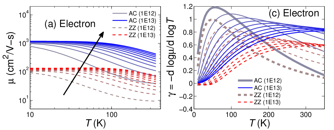

Figure 2(a-b) shows and for electrons and holes in bare phosphorene. As expected, the mobility is about one order of magnitude larger in the armchair direction than in the zigzag direction for both electrons and holes because of the much larger effective masses in the zigzag direction. The electron and hole values are close because . On the other hand, in the zigzag () direction, the electron mobility is higher than the hole mobility because . We also observe that the mobility decreases with temperature for all carrier types and crystal orientations (armchair and zigzag). Like in monolayer MoS2, [13] the mobility drop is carrier density-dependent with the inflection at a lower temperature for lower carrier densities. At any given temperature, the mobility increases monotonically with carrier density, and at room temperature, it varies almost linearly with carrier density. At 300 K, the mobility in cm2V-1s-1 can be fitted to the following empirical formulae
| (5a) | |||||
| (5b) |
where and are the CI impurity and carrier concentration in cm-2, respectively. The first term in Eq. (5a) represents the linear -dependence of the charged impurity-limited carrier mobility that is typical of the 2-dimensional electron gas with parabolic dispersion and weak screening. [35, 22] The second and third terms in Eq. (5a) are corrections taking into account the deviation from the purely linear behavior in lightly and heavily doped samples. Similarly, the mobility in the zigzag direction in Eq. (5a) can be expressed as the sum of a term linearly dependent on and a density-independent term which yields the mobility in undoped phosphorene.
It has been claimed [12, 9] that the phosphorene hole mobility follows a power law i.e. at K because of inelastic phonon scattering. [36] To facilitate the analysis of the temperature dependence, we compute the temperature-dependent exponent by taking numerically the negative logarithmic derivative of the mobility with respect to , i.e. , which at high temperatures ( K) can be interpreted as the power law exponent if the mobility scales as . The results are shown in Fig. 2(c) and (d) for electron and holes, respectively. We observe that is significantly larger for than for for both electrons and holes. At cm-2 and K, () in the armchair (zigzag) direction for both electrons and holes, with being slightly larger for electrons. Thus, is more temperature sensitive than . The relatively large room temperature values of also indicate a significant temperature dependence even in the absence of inelastic phonon scattering. Thus, due caution must be exercised in interpreting the temperature dependence of mobility values from experiments. Electrical characterization of few-layer phosphorene FETs [12] gives which has been construed as a signature of inelastic electron-phonon scattering. However, our result for monolayer phosphorene raises the possibility that CI scattering can play a significant role in the mobility temperature dependence.
Effect of high- oxide encapsulation
Experiments have shown that the use of a high- encapsulating overlayer such as HfO2 can enhance the electron mobility in monolayer MoS2 as well as weakens its temperature dependence. [17] The reason for this mobility enhancement and weaker temperature dependence has been attributed to the dielectric screening of the remote charge impurities by the high- top oxide. [13, 25] We explore the effect of high- oxide encapsulating overlayers such as Al2O3 () and HfO2 () on the CI-limited mobility in phosphorene.
Figure 3 shows and for electrons and holes in Al2O3- and HfO2-covered phosphorene, assuming a CI concentration of cm-2. Comparing Fig. 3(a) and (b) with Fig. 2(a) and (b), the electron and hole mobilities in encapsulated phosphorene are substantially higher because the stronger dielectric screening of the charged impurities by the high- overlayer reduces their effective charge and leads to less CI scattering. The mobility enhancement is even higher for HfO2 [see Fig. 3(c) and (d)] because its dielectric constant is larger () and screens the charged impurities more effectively. This mobility enhancement is especially large at high temperatures and low carrier densities where screening by the polarization charge is weak. For example, from Fig. 2(a) and Fig. 3(a) and (c), we find that = 41, 217 and 461 cm2V-1s-1 at cm-2 and K for electrons in unencapsulated, Al2O3-covered and HfO2-covered phosphorene, respectively i.e. encapsulation enhances the mobility by an order of magnitude. A comparison between Fig. 2(a-b) and Fig. 3 also shows that encapsulation leads a proportionally greater increase in than in .


While the high dielectric environment reduces the effective charge on the charged impurities, it also weakens their polarization charge screening. [13] The latter effect has been used to explain [13] the weaker electron mobility temperature dependence in HfO2-covered monolayer MoS2 relative to bare MoS2. [17] Since the temperature dependence of the mobility in unencapsulated phosphorene is due to the temperature variability of charge screening, we expect the mobility temperature dependence in encapsulated phosphorene to be similarly modified by the high- oxide overlayer.
For a systematic comparison of the temperature dependence, we show the negative logarithmic derivative of the mobility with respect to [i.e. ] as a function of temperature and carrier density for and in Fig. 4. A large magnitude corresponds to a strong mobility temperature dependence while a small magnitude indicates a weak temperature dependence. Comparing Fig. 4(a) with Figs. 4(b) and (c), we find that magnitude of for the phosphorene electrons and holes decreases after encapsulation with Al2O3 or HfO2, over the range of carrier density and temperature values considered. This decrease in the temperature dependence is due to the weakened polarization charge screening.

At low carrier densities ( cm-2), the electron and hole decreases and falls below zero as rises [see Fig. 4(b) and (c)] i.e. the mobility actually increases with temperature for K, which can be most clearly observed for the curves corresponding to cm-2 in Fig. 3(c) and (d). Physically, this is due to the weak polarization charge screening at low carrier densities and high temperatures, which causes the scattering cross section of the charged impurities to be effectively temperature independent. Hence, as the temperature rises, more electron and holes are thermally excited to higher energy states which have a smaller CI scattering cross section and momentum relaxation rate, resulting in a mobility increase. At high carrier densities ( cm-2), the electron and hole is still positive with the range of temperatures considered i.e. the mobility still falls as the temperature increases (see the cm-2 and curves in Fig. 3).
Another consequence of the weaker polarization charge screening is smaller mobility anisotropy. We plot the anisotropy factor for electrons and holes in Fig. 5. In Fig. 5(a), we observe that the anisotropy factor for electrons and holes in unencapsulated phosphorene reaches a maximum of around 10 and 16, respectively, and that it decreases when the carrier density is reduced or when the temperature rises, because a lower carrier density or higher temperature results in weaker charge screening. The dependence of the anisotropy on charge screening can also be seen when we use a high- oxide overlayer. Figure 5(b) shows the anisotropy factor for Al2O3-covered phosphorene. In contrast to the case for unencapsulated phosphorene, the maximum anisotropy at low temperatures is respectively around 7 and 11 for electrons and holes in Al2O3-covered phosphorene, decreasing to around 5 and 6 at room temperature. A similar reduction in the electron and hole anisotropy factor can also be seen in HfO2-covered phosphorene [Fig. 5(c)]. This shows that the anisotropy is significantly dependent on charge screening which varies with temperature, carrier density and dielectric environment. Polarization charge screening enhances more than because the momentum change from CI scattering for carriers moving in the armchair direction is smaller and more heavily screened than in the zigzag direction. Thus, when phosphorene is encapsulated with a high- overlayer, the effect of polarization charge screening is reduced, and the increase in is proportionately larger than the increase in .

Summary
In summary, we have studied the CI-limited mobility ( and ) for electrons and holes in bare and encapsulated monolayer phosphorene. We find that the mobility is highly dependent on the crystal orientation with around an order of magnitude larger than because of the smaller effective electron and hole masses in the armchair direction. The mobility in bare monolayer phosphorene decreases with increasing temperature and decreasing carrier density because of the weaker polarization charge screening of impurities. The same trend can be seen for the mobility anisotropy factor () since the reduced polarization charge screening has a greater negative effect on charge transport in the armchair direction.
We also find that the mobility is more temperature-dependent in the armchair direction than the zigzag direction. When a high- overlayer is used to encapsulate the phosphorene, the carrier mobility is enhanced by up to an order of magnitude because of dielectric screening of the charged impurities. The mobility enhancement from encapsulation is also relatively larger for than for . The dependence of the mobility on carrier density and temperature is reduced by encapsulation because of the weaker polarization charge screening. This also results in smaller mobility anisotropy, which should be detectable in experiments and may be helpful for reducing the orientation dependence in charge transport. Our results suggest that encapsulation is an effective strategy for improving charge transport in monolayer phosphorene.
The authors gratefully acknowledge the financial support from the Agency for Science, Technology and Research (A*STAR), Singapore.
References
- [1] B. Radisavljevic, A. Radenovic, J. Brivio, V. Giacometti, and A. Kis, Nature Nanotechnology 6, 147 (2011).
- [2] Q. Wang, K. Kalantar-Zadeh, A. Kis, J. Coleman, and M. Strano, Nat. Nanotech. 7, 699 (2012).
- [3] H. Qiu, L. Pan, Z. Yao, J. Li, Y. Shi, and X. Wang, Appl. Phys. Lett. 100, 123104 (2012).
- [4] D. Jariwala, V. K. Sangwan, L. J. Lauhon, T. J. Marks, and M. C. Hersam, ACS Nano 8, 1102 (2014).
- [5] H. O. Churchill and P. Jarillo-Herrero, Nat. Nanotech. 9, 330 (2014).
- [6] E. S. Reich, Nature 506, 19 (2014).
- [7] S. P. Koenig, R. A. Doganov, H. Schmidt, A. C. Neto, and B. Oezyilmaz, Appl. Phys. Lett. 104, 103106 (2014).
- [8] H. Liu, A. T. Neal, Z. Zhu, Z. Luo, X. Xu, D. Tománek, and P. D. Ye, ACS Nano 8, 4033 (2014).
- [9] F. Xia, H. Wang, and Y. Jia, Nature Commun. 5, 4458 (2014).
- [10] B. Baugher, H. O. H. Churchill, Y. Yang, and P. Jarillo-Herrero, Nano Lett. 13, 4212 (2013).
- [11] S. Kim, A. Konar, W.-S. Hwang, J. H. Lee, J. Lee, J. Yang, C. Jung, H. Kim, J.-B. Yoo, J.-Y. Choi, Y. W. Jin, S. Y. Lee, D. Jena, W. Choi, and K. Kim, Nat. Commun. 3, 1011 (2012).
- [12] L. Li, Y. Yu, G. J. Ye, Q. Ge, X. Ou, H. Wu, D. Feng, X. H. Chen, and Y. Zhang, Nat. Nanotech. 9, 372 (2014).
- [13] Z.-Y. Ong and M. V. Fischetti, Phys. Rev. B 88, 165316 (2013).
- [14] A. S. Rodin, A. Carvalho, and A. H. Castro Neto, Phys. Rev. Lett. 112, 176801 (2014).
- [15] A. N. Rudenko and M. I. Katsnelson, Phys. Rev. B 89, 201408 (2014).
- [16] D. Jariwala, V. K. Sangwan, D. J. Late, J. E. Johns, V. P. Dravid, T. J. Marks, L. J. Lauhon, and M. C. Hersam, Appl. Phys. Lett. 102, 173107 (2013).
- [17] B. Radisavljevic and A. Kis, Nat. Mater. 12, 815 (2013).
- [18] R. Shishir and D. Ferry, J. Phys.: Condens. Matter 21, 232204 (2009).
- [19] K. Kaasbjerg, K. S. Thygesen, and K. W. Jacobsen, Phys. Rev. B 85, 115317 (2012).
- [20] X. Li, J. T. Mullen, Z. Jin, K. M. Borysenko, M. Buongiorno Nardelli, and K. W. Kim, Phys. Rev. B 87, 115418 (2013).
- [21] Y. Tan, Y. Zhang, K. Bolotin, Y. Zhao, S. Adam, E. Hwang, S. Das Sarma, H. Stormer, and P. Kim, Phys. Rev. Lett. 99, 246803 (2007).
- [22] S. Ghatak, A. N. Pal, and A. Ghosh, ACS Nano 5, 7707 (2011).
- [23] D. Ovchinnikov, A. Allain, Y.-S. Huang, D. Dumcenco, and A. Kis, ACS Nano 8, 8174 (2014).
- [24] Z. Yu, Y. Pan, Y. Shen, Z. Wang, Z.-Y. Ong, T. Xu, R. Xin, L. Pan, B. Wang, L. Sun, et al., Nat. Commun. (In press).
- [25] N. Ma and D. Jena, Phys. Rev. X 4, 011043 (2014).
- [26] W. Zhu, T. Low, Y.-H. Lee, H. Wang, D. B. Farmer, J. Kong, F. Xia, and P. Avouris, Nat. Commun. 5, 3087 (2014).
- [27] T. Low, A. Rodin, A. Carvalho, Y. Jiang, H. Wang, F. Xia, and A. Neto, arXiv:1404.4030 (2014).
- [28] C. Jacoboni, Theory of Electron Transport in Semiconductors (Springer, Berlin, 2010).
- [29] B. Ridley, Quantum processes in semiconductors (Oxford University Press, USA, 1999).
- [30] Q. Li, E. H. Hwang, E. Rossi, and S. Das Sarma, Phys. Rev. Lett. 107, 156601 (2011).
- [31] R. Anicic and Z. L. Miskovic, Phys. Rev. B 88, 205412 (2013).
- [32] Z.-Y. Ong and M. V. Fischetti, Phys. Rev. B 86, 121409 (2012).
- [33] P. F. Maldague, Surf. Sci. 73, 296 (1978).
- [34] K. M. Burson, W. G. Cullen, S. Adam, C. R. Dean, K. Watanabe, T. Taniguchi, P. Kim, and M. S. Fuhrer, Nano Lett. 13, 3576 (2013).
- [35] S. Adam and S. Das Sarma, Phys. Rev. B 77, 115436 (2008).
- [36] A. Morita and T. Sasaki, J. Phys. Soc. Jpn 58, 1694 (1989).