Seebeck effects in two-dimensional spin transistors
Abstract
We consider a spin-orbit-coupled two-dimensional electron system under the influence of a thermal gradient externally applied to two attached reservoirs. We discuss the generated voltage bias (charge Seebeck effect), spin bias (spin Seebeck effect) and magnetization-dependent thermopower (magneto-Seebeck effect) in the ballistic regime of transport at linear response. We find that the charge thermopower is an oscillating function of both the spin-orbit strength and the quantum well width. We also observe that it is always negative for normal leads. We carefully compare the exact results for the linear response coefficients and a Sommerfeld approximation. When the contacts are ferromagnetic, we calculate the spin-resolved Seebeck coefficient for parallel and antiparallel magnetization configuration. Remarkably, the thermopower can change its sign by tuning the Fermi energy. This effect disappears when the Rashba coupling is absent. Additionally, we determine the magneto-Seebeck ratio, which shows dramatic changes in the presence of a the Rashba potential.
I Introduction
One of the key ingredients of spintronics is the possibility of manipulating the electronic flow via spin-charge coupling potentials [1, 2]. This goal can be achieved in semiconductor heterostructures lacking space inversion symmetry, as demonstrated by Rashba [3]. Importantly, the strength of the Rashba spin-orbit interaction can be externally tuned with a gate electrode electrostatically coupled to the heterostructure [4, 5, 6]. Thus, a spin field-effect transistor can be envisaged based on a narrow channel sandwiched between two ferromagnetic electrodes with independently controlled magnetizations [7]. The electric field applied to the gate is then viewed as a momentum-dependent effective magnetic field acting on the channel, causing a modulated precession of the injected spins, which are transmitted into the drain electrode, provided their spin direction matches the drain magnetization. This device works in the ballistic regime and in the single-mode limit, in which case the precession angle is independent of energy.
Recent experiments report signatures of Rashba spin-orbit modulated conductance in spin valve systems [8] measured in the nonlocal configuration [9]. An important difference with the original proposal is that the transistor channel indeed supports multiple modes. As a consequence, conductance oscillations disappear as the spin-orbit coupling increases, a result which is consistent with numerical simulations [10, 11]. The mechanism behind this amplitude decrease is the Rashba intersubband coupling term that mixes adjacent subbands with opposite spin directions [12]. This term cannot be neglected in quantum wires and is responsible for a variety of phenomena: Fano-Rashba antiresonances [13, 14, 15, 16, 17, 18, 19, 20], removal of magnetic-field-induced anomalous conductance steps [21, 22], spin texturing [23, 24, 25, 26, 27, 28, 29, 30], and spin relaxation [31, 32, 33].
In the limit of wide channels, the spectrum of the transversal modes becomes continuous and the Rashba precession and mixing terms must be treated on equal footing. Reference [34] shows that conductance oscillations persist, although they now originate from quantum interference between majority spin propagating states and minority spin quasibound states. These two-dimensional electron systems (2DES) offer the advantage of exhibiting transistor features in nonballistic devices [35] or even without the presence of magnetic contacts [36]. Quite recently, there is a renewed interest in the physics and applications of 2DES due to their bandgap tunability and reduced dimensions [37].
Spintronic devices are attractive systems because they offer new functionalities and less dissipation [38]. However, in contrast to the intense efforts in understanding the electric properties of spin transistors, much less is known about their response to a temperature difference (thermoelectric or Seebeck effect). The subject is interesting in view of recent experiments that verify the generation of spin currents when a thermal gradient is applied. This spin Seebeck effect has thus far been revealed in magnetic alloys [39], ferromagnetic semiconductors [40], and even nonmagnetic materials [41]. In a broad sense, spin caloritronics is the study of spintronic effects created in thermally biased samples [42]. Spin biases due to temperature driven electron flow can be detected by means of the inverse spin Hall effect [43]. Furthermore, a magneto-Seebeck effect has also attracted a good deal of attention recently [44, 45, 46, 47]. Here, the focus is not put on the creation of spin-polarized currents but rather on the dramatic changes seen in the junction thermopower when the orientation of the ferromagnetic electrodes is switched from the parallel to the antiparallel configuration. Finally, recent measurements of the charge thermopower in 2DES setups may indicate the presence of electronic correlations [48, 49] or diffusive transport mechanisms [50, 51].
Our aim in this work is to examine the three Seebeck effects (charge, spin and magneto) in a 2DES spin transistor. We consider a quantum well laterally coupled to two ferromagnetic reservoirs kept at different temperatures , as sketched in Fig. 1. Thermocurrent-induced spin polarization effects in Rashba 2DES are discussed in Refs. [52, 53, 54, 55, 56] using semiclassical approaches. Here, we consider the quantum (ballistic) regime of transport and formulate a theoretical model based on the scattering approach. We observe clear oscillations in the charge Seebeck coefficient when the Rashba strength is varied even when the 2DES is coupled to nonmagnetic reservoirs. Importantly, in this case the transmission for up spins and down spins are equal and hence the spin Seebeck coefficient is identically zero. This result agrees with Ref. [56], which finds an absence of thermospin effects in spin-orbit coupled 2DES. However, we below show that spin imbalances can be created in response to temperature differences when the electrodes are ferromagnetic. The effect is more prominent for larger Rashba splittings.
Remarkably, the Seebeck coefficient shows sign changes as a function of the Fermi energy for the case of magnetic leads. This is one of the main findings of our work, as it suggests the possibility of controlling the thermoelectric current direction by varying the Fermi energy with a nearby gate. Furthermore, the thermopower depends on the relative orientation of the leads’ magnetization. Since the spin-orbit field randomizes the spin direction of current-carrying states, one would expect a quench of the magneto-Seebeck ratio when Rashba interaction is turned on. However, we find significant changes in the presence of spin-orbit coupling.
II Theoretical model
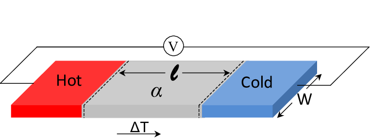
We consider a two-dimensional semiconductor layer in the -plane with a central region of width subjected to a Rashba spin-orbit interaction. In Fig. 1 we show a sketch of our system. The Rashba coupling is spatially varying along the -direction, which we take as the transport direction. The Hamiltonian reads
| (1) |
where is the conduction-band effective mass of the electrons in 2DEG and is the Rashba spin-orbit interaction depending on the Pauli matrices and ,
| (2) |
In Eq. (2) the Rashba strength takes a constant value in each of the three regions of our system. In the left and the right contacts is equal to zero while in the central region, of width , takes a uniform value . In our numerical simulations, the variation of this parameter at the interfaces is almost abrupt with a minor numerical smoothing, see Appendix A.
The eigenfunctions in the leads are plane waves since the reservoirs are assumed metallic with good screening properties. In those asymptotic regions the band structure takes the general form
| (3) |
where and are the wave numbers along (longitudinal) and (transverse) directions, respectively.
The momentum is constant throughout the system since the Hamiltonian of Eq. (1) remains invariant after translation along . Thus, the wave function in the central region can be written in terms of the product of a plane wave in -direction and an -dependent amplitude for each channel labeled with . If we sum over spins and over all the transverse momenta the total wave function reads
| (4) |
where is a spin index that characterizes the spin function , with the usual basis of the Pauli matrices.
To determine the channel amplitude equations we project the Schrödinger equation on a particular channel ,
| (5) | |||||
These channel equations show coupling between different spins due to the spin-orbit interaction (the terms ). However, channels with different remain uncoupled due to the translational invariance along -direction. This a unique feature of 2DES devices since in quantum wires the coupled channel method does connect adjacent modes with opposite spins [13].
In the contacts the Rashba coupling vanishes and the wave functions can be expressed with the aid of input and output amplitudes,
| (6) |
where () for the left (right) lead and we take and . Within scattering theory the output amplitudes are determined from the input ones via reflection and transmission amplitudes,
| (7) |
Here, denotes the opposite contact to . We note that the matrices and of Eq. (7) depend on and they are found after discretizing Eq. (5) on a grid and imposing the boundary conditions given by Eq. (6) with the quantum-transmitting-boundary algorithm [57].

We define the transmission probabilities
| (8) |
where represents the probability that an incident electron in the left lead with spin is transmitted to the right lead with spin . Analogously, is the transmission probability for an electron injected from the right contact with spin to arrive at the left contact with spin . Figure 2 shows the total transmission, , as a function of the Fermi energy for the case at fixed and different lengths of the Rashba region. The mode is interesting since it corresponds to normal incidence, thus dominating the total transmission.
We observe in Fig. 2 that quickly reaches a maximum and then oscillates. This behavior can be nicely understood from the one-dimensional problem of electrons scattering off a square well where is its width and is proportional to its depth. To see this, we set in Eq. (5),
| (9) | |||||
where we choose the quantization axis of the spin in the -direction. Clearly, the two spins are uncoupled. We now make the gauge transformation
| (10) |
Then Eq. (9) is written in terms of
| (11) |
where . For a piecewise constant , Eq. (11) corresponds to the Hamiltonian of a square well of depth . We can readily write the total transmission (summed over spins) as [58]
| (12) |
where is the width of the square well (the spin-orbit region length in our case). Then, is maximum whenever
| (13) |
where . The first maximum of for corresponds to . As we increase the width of the spin-orbit region the first maximum shifts to lower energy, in perfect agreement with Fig. 2. The maximum displacement occurs because should decrease to maintain the condition of Eq. (13) as increases. In the inset of Fig. 2, we represent the total transmission as a function of for fixed values of and . presents maxima at equidistant values of . This can also be simply understood from the resonant condition derived from Eq. (13).

In Fig. 3 we plot as a function of the Fermi energy for at fixed length and different Rashba magnitudes. Similarly to Fig. 2, as increases the first maximum shifts to lower energies. In this case, the analogy with the problem of the square well is based on , which is proportional to the potential depth. Thus, as we increase the value of , the Fermi energy should decrease to fulfil the maxima condition of Eq. (13). The inset of Fig. 3 shows the as a function of for fixed and . Notice that the spacing between maxima increases smoothly because the resonant condition
| (14) |
shows a nonlinear dependence with .
The transmission probabilities for cannot be expressed in closed analytical form because the spins become coupled as illustrated in Eq. (5). It turns out that the contribution of these modes to the total transmission for a given energy is small as electrons are more likely to be refracted from the junction interfaces if . To verify this, let be the spin-transmission summed over all transverse momenta and transmitted spins. Since we consider transport along the longitudinal () direction, we include the projection factor ,
| (15) |
The total projected transmission is thus . In Fig. 4 we compare from Eq. (15) with its contribution. Clearly, the mode contributes more than to the full transmission for most energies. This confirms that with the mode we can understand the basic dynamics of the transmission through our system. For completeness, however, in our calculations we take into account all channels to carefully assess the transport responses.

III Current transport
Within the scattering approach for mesoscopic transport, the current in the direction for a given spin can be written in terms of the transmission found in Sec. II (see Appendix B):
where is the length in the transverse direction and is the momentum in the contacts derived from Eq. (3). Here with are the Fermi-Dirac distribution functions of electrons in each contact with spin ,
| (17) |
with the electrochemical potential and the lead temperature specified below. In cases of common background temperature we denote this by while if no biases are applied . The total current is, finally, .
From the electrochemical potentials ( is the voltage in contact for electrons with spin which accounts for possible population imbalances between different spin subbands) and contact temperatures , we define the temperature difference , the mean electrochemical potential , the bias voltage and the spin bias using the following relations:
| (18a) | |||||
| (18b) | |||||
| (18c) | |||||
| (18d) | |||||
We focus now on the response of our 2D spin transistor to small values of , and . After a Taylor expansion of Eq. (III) up to first order in these shifts, we find
| (19) |
where the transport coefficients and are the linear electric and thermoelectric conductances, respectively. Using Eqs. (18) in Eq. (19), we obtain the total current
| (20) | |||||
and the spin current, defined as ,
| (21) | |||||
Both current expressions are valid in linear response.

In Eq. (19) the electric conductance is given by
| (22) |
where is the unit of conductance for a 2DES length along . Physically, is thus a spin-resolved conductance per unit of transverse length. Hence, the total conductance is . In the zero temperature limit, the conductance per spin reads
| (23) |
where .
The linear thermoelectric conductance in Eq. (19) reads
where is the natural scale of the thermoelectric response of a 2DES of width . The total thermoelectric conductance is . At very low temperatures, a Sommerfeld expansion [59] yields
| (25) |
where the derivative is defined as .
Figure 5 presents the total electric and thermoelectric conductances as a function of the Fermi energy from a calculation of Eqs. (23) and (25), respectively. The transmission is determined from a full evaluation of Eq. (15). We find that the electric conductance (black solid line) is an monotonically increasing function of . At sufficiently large energy values, goes as because the transmission approaches its maximum value when (see Figs. 2 and 3). Only at low energies presents a small deviation from this behavior, which is much more visible when we calculate the thermoelectric conductance (red dashed line). While at high energies approaches zero as as dictated by Eq. (25), the thermoelectric conductance shows a peak at low values of .
The insets of Fig. 5 depict and as a function of the spin-orbit region width (top panel) and the Rashba coupling intensity (bottom panel). We observe that both responses are strongly modulated and present maxima at fixed values. This originates from the transmission oscillations discussed in Sec. II as a function of or . Interestingly, our device works as a current modulator in response to voltage or temperature biases applied to normal leads. This is in contrast with the spin transistor proposal of Ref. [7]. Our system (both the leads and the 2DES channel) is entirely nonmagnetic. It is precisely due to this reason that and and no spin polarization is possible.
IV Charge and spin thermopower
In Eq. (25) we find that the thermoelectric conductance comprises two terms at low temperature, in contrast to the electric conductance, Eq. (23), which consists of a single term. With the aim to understand more clearly this additional contribution we calculate the charge thermopower or Seebeck coefficient, . determines the voltage generated in the junction in response to a temperature shift under open circuit conditions. Then, from Eqs. (20) and (21), we find
| (26) |

Inserting Eqs. (23) and (25) in Eq. (26), we obtain the low-temperature thermopower,
| (27) |
The Seebeck coefficient is measured in units of . We observe two contributions in Eq. (27). The first term is constant and represents an intrinsic contribution to the entropy per unit charge of thermally excited electrons. It is independent of the scattering potential and the sample details. The second term, , is a purely transport contribution that arises from the energy dependence of the transmission function. Interestingly, the first term is unique to 2DES since in quasi-onedimensional systems (quantum point contacts) and quasi-zerodimensional systems (quantum dots) this contribution is absent. Therefore, the intrinsic term can be explained as a dimensionality effect which also shows up in, e.g., graphene monolayers [60]. The only difference is that in graphene is doubled because its energy dispersion is linear, , unlike the quadratic dependence in our semiconductor 2DES [Eq. (3)]. In fact, if we use the function defined in Eqs. (23) we can recast Eq. (27) as a Mott-like formula,
| (28) |
The difference with the formula discussed in Ref. [61] is that our Eq. (28) is valid in the ballistic regime of quantum transport.

We analyze the relative importance between the intrinsic and the transport terms. To visualize this, Fig. 6 shows the different contributions as a function of the Fermi energy. In general, both have comparable strengths and should then be treated on equal footing. Note that is always negative because the generated voltage tends to counteract the thermal bias. Below, we will show deviations of this behavior when the sample is attached to ferromagnetic contacts. In Fig. 6 grows as and quickly goes to zero. On the other hand, although the overall trend of is similar to the intrinsic term, we observe in a stronger effect due to the potential scattering at low energy. Finally, we recall that both and present oscillations as a function of and , see insets (a) and (b) of Fig. 5. The thermopower, which is the ratio between the thermoelectric and electric conductances, also presents these oscillations as seen in the insets (a) and (b) of Fig. 6. Importantly, the oscillations are due to the transport term since is independent of and .
We note in passing that the main properties of discussed above can be also detectable in heat current measurements. Due to Onsager reciprocity, the electrothermal conductance (Peltier effect) is directly connected to the thermoelectric conductance (Seebeck effect), see App. C. Moreover, we show in App. C that the Wiedemann-Franz law holds at low temperature. Then, it is natural to ask to what extent the Sommerfeld approximation is valid. To do so, we compare the results of Eqs. (22) and (III), i.e., the exact calculation at , with Eqs. (23) and (25), which are valid at very low temperature. The difference between the exact and Sommerfeld calculation of the thermoelectric conductance is shown in the inset of Fig. 7. At low energies, , there exists a small deviation between the exact curve and the Sommerfeld result. This confirms that the Sommerfeld expansion is no longer valid when . The main panel of Fig. 7 presents the deviation of the Sommerfeld calculation (dashed curve) for the Seebeck coefficient compared with the exact value (solid curve) as a function of the background temperature. In the Sommerfeld expansion, depends linearly with as shown in Eq. (27). Therefore, for high temperatures such that the Sommerfeld approximation is not valid.
We end this section considering the spin Seebeck coefficient . When we apply a temperature gradient across the junction, it can also lead to spin accumulations in the leads. Then, the spin Seebeck coefficient determines the spin voltage generated in the junction in response to a temperature shift when both the charge and the spin currents are set to zero. From Eqs. (20) and (21) we obtain
| (29) |
For normal leads the spin Seebeck is identically zero since the system is nonmagnetic and the spin polarization is not possible. We consider in the next section a 2DES coupled to ferromagnetic leads, a system where does not necessarily vanish.
V Ferromagnetic contacts
The case of ferromagnetic contacts is relevant for spin-injection problems in ferromagnet-semiconductor junctions [1]. We describe the contacts with the Stoner-Wohlfarth model for itinerant ferromagnetism. The electronic bands for opposite spins become split due to exchange interaction between carriers. Then, the Hamitonian reads
| (30) |
where is the magnetization direction in which the leads are polarized, is the spin vector and is the Stoner splitting, which is finite in the -positions of the leads only. For metallic electrodes, is of the order of a few eV, introducing serious conductivity mismaches at the junction [62], a problem which can be mitigated using tunnel barriers [63]. For the present discussion, it is more convenient to consider spin injectors made of diluted magnetic semiconductor compounds, which show giant Zeeman splittings up to meV for moderate values of external magnetic fields [64]. For definiteness, we consider in Eq. (30) an energy shift that eases the spin transport analysis. In particular, this shift eliminates the effect of a potential mismatch and can be experimentally implemented with a potential gating of the central regions.
In the same way of the piecewise constant function in Sec. II, we take a uniform in each of the three parts of our system: nonzero in the contacts and vanishingly small in the 2DES. For the numerical implementations, the interfaces are described with slightly smoothed functions, see App. A. We investigate two different orientation schemes: parallel (P) and antiparallel (AP) configurations as sketched in the insets of Fig. 8. The case of parallel polarization corresponds to whereas the antiparallel case results from , where is half of the absolute Zeeman splitting. In what follows, we take the polarization in the -direction: . Thus, we define a potential in the leads,
| (31) |
where labels the spin in the -direction. Then, for the P configuration the electrons with (minority spins) are confined by a potential well of width (the separation between contacts, see App. A) while those with feel no potential as they travel (majority spins). In the AP configuration both types of carrier experience a potential step but localized in opposite contacts. Due to the differing potential landscapes, we expect strong changes as compared with the nonmagnetic case treated in the previous sections.

The dispersion relation on the contacts generalizes Eq. (3) conveniently modified to account for the Stoner field:
| (32) |
Importantly, the total momentum now depends on both the contact and the spin. As a consequence, since the -momentum remains invariant, we find
| (33) |
The channel amplitude equation expressed in Eq. (5) keeps the same form, with the only addition of the spin dependent potential and the replacement in the asymptotic conditions Eq. (6). From the resulting expression we calculate the new probability transmissions and obtain, finally, the total current in the propagation direction,
where follows from Eq. (33) with taken for convenience (the current conservation condition is always fulfilled). The electric and thermoelectric conductances in the limit of linear response are obtained in the same manner as in Sec. III. At very low temperature, they read
| (35a) | |||||
| (35b) | |||||

In Fig. 8 we present the total electric conductance, , as a function of . We distinguish between P (a) and AP (b) polarizations of the magnetic leads. Consider first the case without spin-orbit interaction (). For parallel orientation the majority electrons are not scattered back while the minority electrons feel a potential well of depth . Then, when we only have one propagating spin channel, , and the conductance is given simply by the number of open channels, which scales as discussed in Sec. III. For the propagating mode becomes active. Thus, the potential causes the transmission to oscillate with energy. These oscillations are akin to the Ramsauer oscillations in electron scattering [65]. This can be more clearly seen in Fig. 9(a), which depicts the behavior separately for and . The majority spins contributes to with a -dependent function while the minority spins do not attain a nonzero until . Above this energy threshold, the electrons with spin lead to smooth oscillations of due to the Ramsauer effect. In the antiparallel case [Fig. 8(b)], the conductance is zero below the energy threshold for both spin indices, see Fig. 9(c), since electrons are reflected back from the step potential at the right junction according to Eq. (31) while electronic channels with are not active for due to the step potential at the left contact.

Turning on the spin-orbit potential alters the previous picture. For energies below the threshold, Fig. 8 shows a different type of oscillation independently of the leads’ magnetic orientation. These are due to resonant Fano interference between the propagating spins and the quasibound states of opposite spins trapped between the polarized contacts [13, 34]. Figure 9(b) shows that the Fano oscillations in the P case are only possible for electrons with spin since for the electrons are evanescent states. At higher energies the two modes become propagating states and the Fano oscillations vanish. In the AP case, the oscillations also appear for but these are now due to electrons with undergoing multiple reflections between the junctions since minority electrons are inactive for transport until [34].

Figure 10 shows the thermoelectric conductance as a function of Fermi energy for both P and AP configurations. According to Eq. (35b), can be written as a function of the energy derivative of the electric conductance. As a consequence, the Rashba induced oscillations for become largely amplified for . Remarkably, the curves cross the horizontal axis, taking positive and negative values, whereas the case always gives . Therefore, the combined influence of ferromagnetic leads and spin-orbit interaction can drive the electronic current either from the hot to the cold reservoir (as in the normal case, see Fig. 5) or, notably, from the cold to the hot reservoir. The latter phenomenon is independent of the relative magnetic orientation (parallel or antiparallel), the main difference being that below the energy threshold the thermoelectric conductance vanishes in the AP case , similarly to the electric conductance [Fig. 8(b)]. Finally, for high energies smoothly decays to zero since the transmission becomes weakly energy dependent for . This demonstrates that the spin-orbit interaction in 2D spin transistors leads to stronger effects for energies lower than the Zeeman splitting.
We depict in Fig. 11 the spin-resolved thermoelectric conductances. As expected, the large amplitude oscillations in the P case arise in the majority spin channel only [Fig. 11 (a)]. For the Ramsauer-like oscillations are visible above the energy threshold in the minority channel [Fig. 11 (c)]. In the antiparallel case, the thermoconductances obey and attain their highest value when reaches because the transmission variation is largest at that point, as both spin channels become propagating [Fig. 11 (d)]. In Fig. 11 (b) the Ramsauer-like oscillations are also visible for .
The thermopower obeys Eq. (28) but now is calculated from Eq. (35a). In Fig. 12 we plot the charge Seebec coefficient , for both P (a) and AP (b) configurations. For , is almost zero. Only for energies slightly higher than we observe a dip that correlates with the thermoelectric conductance peak observed in Fig. 10. In contrast to the normal case depicted in Fig. 6, here oscillates and changes its sign for . This indicates that at given temperature difference, depending on the value of we can generate positive or negative thermovoltages. This is a very interesting effect since without ferromagnetic contacts the thermopower is always negative. We need to introduce both a Zeeman spliting and a spin-orbit interaction to generate the sign oscillations in , which are more intense for AP configurations. We emphasize that although thermopower sign changes can be detected in quantum dots [66, 67] or molecular transistors [68], the effect discussed here occurs in an extended 2D system.

To determine the spin Seebeck coefficient at low temperature, we introduce Eq. (35) in Eq. (29), obtaining
where . Here, the spin indices follow the quantization axis established by the leads’ magnetization, i.e., the -direction. Unlike the normal case, we now expect nonzero values of since, quite generally, . Figure 12(c) shows the results for the parallel configuration in the case with (red curve) and without (black curve) Rashba interaction. We observe that for the spin Seebeck coefficient presents a smooth behavior and only at energies slightly larger than the Ramsauer-like oscillations arise.
When the Rashba coupling is active, changes its sign alternatively for . This indicates that at fixed value of depending on we can generate a positive or negative spin voltage . The case for the AP configuration is plotted in Fig. 12(d). For zero Rashba coupling since the spin components of the electric and thermoelectric conductance are equivalent, see Figs. 9(c) and 11(d). With nonzero value of we recover the oscillations for , with an amplitude larger than for the charge case [Figure 12(b)]. The oscillations in are more intense for the AP than for the P configuration. It is due to a spin valve effect, i.e., for we do not find any active channel for the AP configuration, while for the P configuration the mode is open. Hence, for the electric conductance takes lower values for the AP configuration than for the parallel one. As a consequence, , which is inversely proportional to , attains higher values.

The magneto-Seebeck effect is a spintronic phenomenon that gives rise to changes in the thermopower of a magnetic junction upon switching the leads’ magnetic moments [44]. In Fig. 12(a) and (b) we found that the thermopower significantly changes during the transition from P to AP configurations. Then, it is natural to quantify this departure by defining the magneto-Seebeck coefficient as
| (37) |
where and are the thermopower in the parallel and antiparallel configuration, respectively. Figure 13 shows the magneto-Seebeck coefficient as a function of the Fermi energy for (black curve) and (red curve). When the Rashba coupling is absent, is closer to zero and only for energies slightly exceeding a peak arises since the two spin channels are open and we have an increase of the electric conductance. Conspicuously, for a finite value of the magneto-Seebeck coefficient presents oscillations and sign changes, much like the thermopower oscillations discussed above. This supports the suggestion that the charge thermopower can be controlled by changing the relative magnetization orientation. While the experiment reports sign changes of as a function of the base temperature [44], we here predict a similar effect by tuning the Fermi energy of the 2DES device.
VI Conclusions
We have discussed the quantum thermoelectric properties of a two-dimensional electron system with nonhomogeneous spin-orbit interaction. When the device is attached to normal electrodes, we find that the thermopower is strongly modulated by either the spin-orbit strength or the channel length at fixed Fermi energy. In the case of ferromagnetic leads, we distinguish between charge, spin and magneto-Seebeck effects. Interestingly, the thermoelectric dynamics is dominated by quantum interference effects for energies below the Zeeman splitting in the leads. These effects lead to large amplitude oscillations of the different thermopowers that change their sign as the Fermi energy increases. The number of observed oscillations can be tuned with the separation between contacts. Importantly, the Seebeck coefficients depend on the relative orientation of the magnetic moments in the leads, causing sizeable values of the magneto-Seebeck coefficient. In general, we demonstrate that a semiconductor two-dimensional electron system offers quite remarkable capabilities for the generation of highly tunable thermoelectric properties.
Our results may be also relevant for spin transistors built with two-dimensional electron systems other than semiconductor heterostructures: silicon [69, 70], graphene [71, 72, 73, 60, 74] or metal dichalcogenides [74]. Further extensions of our model should consider the quasi-one-dimensional case, which is important for quantum wires and carbon nanotubes. Another crucial aspect in modeling realistic ferromagnetic-tunnel junctions is the presence of tunnel barriers, which might alter the predictions discussed in this paper. Future works should also consider disorder effects, which are relevant in 2D systems with low mobility [75], and nonlinear features as those observed in the dc resistivity of quantum Hall conductors [76].
Acknowledgments
This work has been supported by MINECO under Grant No. FIS2011-23526.
Appendix A Interfaces
This appendix contains the mathematical expressions of and employed in our numerical simulations for the interfaces. We model the step-like character of these quantities using Fermi-like functions
| (38) |
where is the junction position of the step and determines the length around where the transition takes place. Then,
| (39) | |||||
where the Rashba strength and the Zeeman splitting are constants. Our results are independent of the interface details because we take sharp transitions, i.e., . In our numerical calculations we take , and .
Appendix B Current expression
We obtain the current flowing along -direction from:
| (41) |
where is a sum over the transmitted spin and a sum over all the possibles momenta on the -direction. Here with are the Fermi-Dirac distribution functions of electrons in each contact with spin [Eq. (17)] and the transmission probability from subband with spin to subband with spin .
In the continuum limit we make the replacement:
| (42) |
where is the width of the sample in the -direction and with the momentum magnitude and the incident angle. Using this relation,
| (43) | |||||
Appendix C Heat transport
The stationary heat current (say, at the right contact) is given by:
| (44) | |||||
where is the chemical potential in the right contact at given spin . The sum of the right and the left heat current gives the dissipated Joule heating, .
We apply a small voltage bias which, after Taylor expanding up to first order in , gives the electrothermal conductance
| (45) |
at very low values of . Here, . Comparing with Eq. (25), we check that the Klein-Onsager relation, , is fulfilled as expected.
The thermal conductance, , is obtained in linear response when a small temperature difference is applied across the junction. At low temperatures we find:
| (46) |
where . Then, the Wiedemann-Franz law is satisfied since .
References
- [1] J. Fabian, A. Matos-Abiague, C. Ertler, P. Stano, and I. Zutic, Acta Phys. Slov. 57, 565 (2007).
- [2] M. Johnson and R.H. Silsbee, Phys. Rev. Lett. 55, 1790 (1985).
- [3] E. I. Rashba, Fiz. Tverd. Tela (Leningrad) 2, 1224 (1960) [Sov. Phys. Solid State 2, 1109 (1960)].
- [4] J. Nitta, T. Akazaki, H. Takayanagi, and T. Enoki, Phys. Rev. Lett. 78, 1335 (1997).
- [5] G. Engels, J. Lange, Th. Schäpers, and H. Lüth, Phys. Rev. B 55, R1958 (1997).
- [6] D. Grundler, Phys. Rev. Lett. 84, 6074 (2000).
- [7] S. Datta and B. Das, Appl. Phys. Lett. 56, 665 (1990).
- [8] H. C. Koo, J. H. Kwon, J. Eom, J. Chang, S. H. Han, and M. Johnson, Science 325, 1515 (2009).
- [9] F. J. Jedema, H. B. Heersche, A. T. Filip, J. J. A. Baselmans, and B. J. van Wees, Nature 416, 713 (2002).
- [10] M. M. Gelabert, L. Serra, D. Sánchez, and R. López, Phys. Rev. B 81, 165317 (2010).
- [11] A. N. M. Zainuddin, S. Hong, L. Siddiqui, S. Srinivasan, and S. Datta, Phys. Rev. B 84, 165306 (2011).
- [12] F. Mireles and G. Kirczenow, Phys. Rev. B 64, 024426 (2001).
- [13] D. Sánchez and L. Serra, Phys. Rev. B 74, 153313 (2006).
- [14] J.-S. Jeong and H.-W. Lee, Phys. Rev. B 74, 195311 (2006).
- [15] L. Zhang, F. Zhai, and H. Q. Xu, Phys. Rev. B 74, 195332 (2006).
- [16] C. A. Perroni, D. Bercioux, V. Marigliano Ramaglia, and V. Cataudella, J. Phys.: Condens. Matter 19, 186227 (2007).
- [17] K. Shen and M.W. Wu, Phys. Rev. B 77, 193305 (2008).
- [18] D. Sánchez, Ll. Serra, and M.-S. Choi, Phys. Rev. B 77, 035315 (2008).
- [19] P. A. Orellana, M. Amado, and F. Domínguez-Adame, Nanotechnology 19, 195401 (2008).
- [20] K. E. Nagaev and A. S. Goremykina, Phys. Rev. B 89, 035436 (2014).
- [21] L. Serra, D. Sánchez, and R. López, Phys. Rev. B 72, 235309 (2005).
- [22] C. H. Quay, T. L. Hughes, J. A. Sulpizio, L. N. Pfeiffer, K. W. Baldwin, K. W. West, D. Goldhaber-Gordon, and R. de Picciotto, Nature Phys. 6, 336 (2010).
- [23] W. Haüsler, Phys. Rev. B 63, 121310 (2001).
- [24] M. Governale and U. Zülicke, Phys. Rev. B 66, 073311 (2002).
- [25] E. Ya. Sherman, A. Najmaie, and J. E. Sipe, Appl. Phys. Lett. 86, 122103 (2005).
- [26] S. I. Erlingsson, J. C. Egues, and D. Loss, Phys. Status Solidi C 3, 4317 (2006).
- [27] P. Upadhyaya, S. Pramanik, S. Bandyopadhyay, and M. Cahay, Phys. Rev. B 77, 045306 (2008).
- [28] P. Stefanski, J. Phys.: Condens. Matter 22, 505303 (2010).
- [29] M. Malard, I. Grusha, G. I. Japaridze, and H. Johannesson, Phys. Rev. B 84, 075466 (2011).
- [30] P. Wojcik, J. Adamowski, B. J. Spisak, and M. Woloszyn, J. Appl. Phys. 115, 104310 (2014).
- [31] A. A. Kiselev and K. W. Kim, Phys. Rev. B 61, 13115 (2000)
- [32] E. Ya. Sherman and J. Sinova, Phys. Rev. B 72, 075318 (2005).
- [33] M. W. Wu, J. H. Jian, and M. Q. Weng, Phys. Rep. 493, 61 (2010).
- [34] M. M. Gelabert and L. Serra, Eur. Phys. J. B 79, 341 (2011).
- [35] J. Schliemann, J. C. Egues, and D. Loss, Phys. Rev. Lett. 90, 146801 (2003).
- [36] K. C. Hall, W. H. Lau, K. Gundogdu, M. E. Flatté, and T. F. Boggess, Appl. Phys. Lett. 83, 2937 (2003).
- [37] G. Fiori, F. Bonaccorso, G. Iannaccone, T. Palacios, D. Neumaier, A. Seabaugh, S. K. Banerjee, and L. Colombo, Nature Nanotech. 9, 768 (2014).
- [38] D. D. Awschalom and M. E. Flatté, Nature Phys. 3, 153 (2007).
- [39] K. Uchida, S. Takahashi, K. Harii, J. Ieda, W. Koshibae, K. Ando, S. Maekawa, and E. Saitoh, Nature (London) 455, 778 (2008).
- [40] C.M. Jaworski, J. Yang, S. Mack, D. D. Awschalom, J. P. Heremans, and R. C. Myers, Nature Mater. 9, 898 (2010).
- [41] C.M. Jaworski, R. C. Myers, E. Johnston-Halperin, and J. P. Heremans, Nature (London) 487, 210 (2012)
- [42] G.E.W. Bauer, A.H. MacDonald and S. Maekawa, Solid State Commun. 150, 459 (2010).
- [43] E. Saitoh, M. Ueda, H. Miyajima, and G. Tatara, Appl. Phys. Lett. 88, 182509 (2006).
- [44] M. Walter, J. Walowski, V. Zbarsky, M. Münzenberg, M. Schäfers, D. Ebke, G. Reiss, A. Thomas, P. Peretzki, M. Seibt, J. S. Moodera, M. Czerner, M. Bachmann, and C. Heiliger, Nat. Mater. 10, 742 (2011).
- [45] J. M. Teixeira, J. D. Costa, J. Ventura, M. P. Fernandez-Garcia, J. Azevedo, J. P. Araujo, J. B. Sousa, P. Wisniowski, S. Cardoso, and P. P. Freitas, Appl. Phys. Lett. 102, 212413 (2013).
- [46] C. López-Monís, A. Matos-Abiague, and J. Fabian, Phys. Rev. B 89, 054419 (2014).
- [47] A. Boehnke, M. Milnikel, M. Walter, V. Zbarsky, C. Franz, M. Czerner, K. Rott, A. Thomas, C. Heiliger, and M. Münzenber, and G. Reiss, arXiv:1405.1064 (preprint).
- [48] V. Narayan, M. Pepper, J. Griffiths, H. Beere, F. Sfigakis, G. Jones, D. Ritchie, and A. Ghosh, Phys. Rev. B 86, 125406 (2012).
- [49] V. Narayan, E. Kogan, C. Ford, M. Pepper, M. Kaveh, J. Griffiths, G. Jones, H. Beere, and D. Ritchie, New J. Phys. 16, 085009 (2014).
- [50] W. E. Chickering, J. P. Eisenstein, and J. L. Reno, Phys. Rev. Lett. 103, 046807 (2009).
- [51] A. Ganczarczyk, S. Rojek, A. Quindeau, M. Geller, A. Hucht, C. Notthoff, J. König, A. Lorke, D. Reuter, and A. D. Wieck, Phys. Rev. B 86, 085309 (2012).
- [52] Z. Ma, Solid State Comm. 150, 510 (2010).
- [53] C. M. Wang and M. Q. Pang, Solid State Comm. 150, 1509 (2010).
- [54] A. Dyrdal, M. Inglot, V. K. Dugaev, and J. Barnaś, Phys. Rev. B 87, 245309 (2013).
- [55] J. Borge, C. Gorini, and R. Raimondi, Phys. Rev. B 87, 085309 (2013).
- [56] P. E. Iglesias and J. A. Maytorena, Phys. Rev. B 89, 155432 (2014).
- [57] C. S. Lent and D. J. Kirkner, J. Appl. Phys. 67, 6353 (1990).
- [58] See, e.g., D. J. Griffiths, Introduction to Quantum Mechanics, 2nd ed., Pearson Prentice Hall, Upper Saddle River, New Jersey (2005), p. 82.
- [59] N. W. Ashcroft and N. D. Mermin, Solid State Physics, Saunders College, Philadelphia (1976), pp. 253–-258.
- [60] M. I. Alomar and D. Sánchez, Phys. Rev. B 89, 115422 (2014).
- [61] M. Cutler and N. F. Mott, Phys. Rev. 181, 1336 (1969).
- [62] G. Schmidt, D. Ferrand, L. W. Molenkamp, A. T. Filip, and B. J. van Wees, Phys. Rev. B 62, R4790 (2000).
- [63] E. I. Rashba, Phys. Rev. B 62, R16267 (2000).
- [64] A. Slobodskyy, C. Gould, T. Slobodskyy, G. Schmidt, L.W. Molenkamp, D. Sánchez, Appl. Phys. Lett. 90, 122109 (2007).
- [65] M. Cahay, S. Bandyopadhyay, Phys. Rev. B 68, 115316 (2003).
- [66] A. A. M. Staring, L. W. Molenkamp, B. W. Alphenaar, H. van Houten, O. J. A. Buyk, M. A. A. Mabesoone, C. W. J. Beenakker, and C. T. Foxon, Europhys. Lett. 22, 57 (1993).
- [67] S. Fahlvik Svensson, E. A. Hoffmann, N. Nakpathomkun, P. M. Wu, H. Q. Xu, H. A. Nilsson, D. Sánchez, V. Kashcheyevs and H. Linke, New J. Phys. 15, 105011 (2013).
- [68] P. Reddy, S. Y. Jang, R. A. Segalman, and A. Majumdar, Science 315, 1568 (2007).
- [69] I. Appelbaum, B. Huang, and D. J. Monsma, Nature (London) 447, 295 (2007).
- [70] C. L. Dennis, C. Sirisathitkul, G. J. Ensell, J. F. Gregg and S. M. Thompson, J. Phys. D: Appl. Phys. 36, 81 (2003).
- [71] S. Cho, Y.-F. Chen, and M. S. Fuhrer, Appl. Phys. Lett. 91, 123105 (2007).
- [72] Y. G. Semenov, K. W. Kim, and J. M. Zavada, Appl. Phys. Lett. 91, 153105 (2007).
- [73] M.-K. Lee, N.-Y. Lue, C.-K. Wen, and G. Y. Wu, Phys. Rev. B 86, 165411 (2012).
- [74] A. Dankert, L. Langouche, M. V. Kamalakar, and S. P. Dash, ACS Nano 8, 476 (2014).
- [75] T. Ando, A. Fowler, and F. Stern, Rev. Mod. Phys. 54, 437 (1982).
- [76] C. L. Yang, J. Zhang, R. R. Du, J. A. Simmons, and J. L. Reno, Phys. Rev. Lett. 89, 076801 (2002).