Memory effect in ferroelectric single electron transistor: violation of conductance periodicity in the gate voltage
Abstract
The fundamental property of most single-electron devices with quasicontinuous quasiparticle spectrum on the island is the periodicity of their transport characteristics in the gate voltage. This property is robust even with respect to placing the ferroelectric insulators in the source and drain tunnel junctions. We show that placing the ferroelectric inside the gate capacitance breaks this periodicity. The current-voltage characteristics of this SET strongly depends on the ferroelectric polarization and shows the giant memory-effect even for negligible ferroelectric hysteresis making this device promising for memory applications.
pacs
77.80.-e,72.80.Tm,77.84.LfI Introduction
Ferroelectricity like magnetism has been under investigation for a decades. Recent progress in ferroelectricity is stimulated by i) miniaturisation of ferroelectric samples to nanoscale where they show new physical properties compared to the bulk ferroelectric materials, [1, 2, 3, 4, 5, 6, 7, 8, 9, 10, 11, 12, 13, 14] and ii) modern computer processors and memory demand storing and moving electric charges, and control associated electric fields. There is a tendency for further increase of computer efficiency that results in facing the nanolevel with individual electrons and atoms. In ferroelectric materials polarization is produced by atom displacements. Nanoferroelectrics combined with single electron-nanocircuits are thus promising devices for memory storage and information processing.
Recently it was shown that the presence of ferroelectricity in the source and drain tunnel junctions of single electron transistor (SET) induces memory effect in the current-voltage characteristics even in the limit of negligible hysteresis of the ferroelectric insulators. [15] The bottle-neck of ferroelectric SET is the experimental difficulty to produce ultrathin and ultra small ferroelectric tunnel junctions with special parameters. Technologically it is much easier to produce a nanothin ferroelectric layer but not thin enough for perfect electron tunneling. Such layer can be placed into the gate capacitance of the SET. From the first glance physics of such ferroelectric should be similar to physics of SET considered in Ref. 15 with ferroelectric source and drain capacitors. But this is not so.
The fundamental property of most single-electron devices with quasicontinuous quasiparticle spectrum on the island is the periodicity of their transport characteristics in the gate voltage. This property is robust even with respect to placing the ferroelectric insulators in the source and drain tunnel junctions. [15] We show that placing the ferroelectric inside the gate capacitance breaks this periodicity even for negligible ferroelectric hysteresis. Applying relatively small “switching” gate voltage one can change the polarization of ferroelectric. We show that further increase of the gate voltage does not affect the direction of ferroelectric polarization. The current-voltage characteristics of this SET strongly depends on the ferroelectric polarization and shows the memory-effect making this device promising for memory applications.

II Single electron transistor with ferroelectric gate
II.1 The Model
The ferroelectricity localized in the gate-capacitance changes the distribution of the excess charge in the nano-grain. In the absence of quantum fluctuations the grain charge is . Here is excess charge number, is the elementary charge, is the potential of the nano-grain, with are the capacitances and is the grain surface. The surface integration is performed over the nano-grain part which is in contact with the ferroelectric. The polarization itself depends on the grain charge. Thus, calculations of the charge statistics and polarization should be done self-consistently. [15]
Generally the electric field dependence of polarization in SET has hysteresis. The following model takes this effect into account
| (1) |
where “u” and “d” stands for the upper and lower branches of hysteresis loop, is the saturation field, is the saturation polarization amplitude, describes the width of the hysteresis loop. Similarly we can write the voltage dependence of the polarization introducing and where is the width of the gate capacitor: . The typical graph of is shown in Fig. 2.

In typical single-electron devices the electron tunneling is a much faster process then the relaxation of the ferroelectric. [15] This is related to the fact that ferroelectricity is related to the shift of ions that are heavy and inert. Therefore the ferroelectric in SET is sensitive to the average electric field over the “fast” electron-tunneling events. [15] Thus, for a fixed ferroelectric polarization we can calculate the average grain potential . Since itself depends on the polarization through the probability distribution to find excess charges on the grain we obtain the self-consistency equation. The probabilities itself can be calculated using the modified SET Orthodox theory, see Ref. 15 and Refs. 16, 17, 18 where selfconsistency was developed for SET with slowly oscillating gate electrode.

II.2 Dimensionless units and basic notations
SET has a number of important parameters. It is convenient to use the following units for analytical and numerical calculations: is the energy and temperature unit (), the elementary charge is the charge-unit (electron charge is equal ). The capacitance becomes dimensionless using , so . We use the (bare) tunnelling resistance of the first tunnel junction, , between the left electrode and the nanograin as the unit for the resistance. Also we use the effective gate charge as a control parameter, .
III Ferroelectric SET at low temperatures. Orthodox theory.
Here we consider the limit of low temperatures, where transport properties of SET (not far from the degeneracy points) are well described by the “orthodox model”. [19, 20, 21, 22] Generalization of the orthodox model for SET with ferroelectricity was recently formulated in Ref. 15. Using equations of Ref. 15 one can find the distribution functions describing the excess charge statistics on the grain, the mutual dependence of ferroelectric polarization, the charge statistics and electron current.
III.1 Ferroelectric with ultrathin hysteresis loop
First we consider the limiting case of ultrathin ferroelectric hysteresis loop, with in Eq. (1). Also we assume that the parameter in Eq. (1). Using these assumptions we explain the strong influence of ferroelectricity in the gate capacitor on the fundamental property of SET: periodicity of its transport properties in the gate voltage .
III.1.1 Ferroelectric with small switching field:
The basic features of SET with ferroelectricity in the gate capacitor can be qualitatively understood for small switching field, .
First we investigate the SET for zero driving voltage, , and zero switching voltage, . We also assume that electrons do not hop between leads and the grain. This assumption is reasonable for gate voltage being away from the points of intersection of different free energy branches. In this case the charge number on the grain does not fluctuate and the average potential is equal to the instant potential and . The equation describing the potential has the form
| (2) |
Here . Equation 2 has the following solution in the limit :
| (3) |
Each branch of potential has three regions. Two regions have the same slope but their shifted by the voltage . The transition between these regions is located in the vicinity of the point with the width of . For parameter the different branches do not intersect while for the branches intersect on the line . The intersection of with is happening at the point .
Following the orthodox theory we introduce the effective free energy of the SET
| (4) |
For zero polarization, , the function is a parabola in parameter . At finite the ferroelectric polarization depends on the parameter making the function more complicated function consisting of parabola fragments separated by some transition region, see Fig. 3. At the degeneracy points, where the function intersects, the Coulomb blockade is suppressed allowing electrons go through the SET from one lead to another. The positions of these degeneracy points, corresponding to the conductivity maximums, is . Thus, all the conductivity peaks move to the zero gate voltage point. If a peak reaches the point it stays at this point with further increase of parameter . All peaks have the same shift magnitude, but different direction for peaks below and above the point . This leads to the breaking of periodicity in the conductivity peaks of FE SET. The numerically calculated conductance peaks approximately correspond to the degeneracy points as shown in Fig. 3.
In orthodox theory the conductance of SET (without ferroelectricity) at low temperatures, , is
| (5) |
Here is the deviation of the induced charge by the gate terminal from the nearest degeneracy point. With ferroelectricity in the gate, we should replace the deviation by
| (6) |
This equation is valid for small parameter . For small switching voltage, , we can replace in Eq. (6) by unity and using Eq. (5) find that the conductance peaks are shifted by for and by for . This is consistent with numerical calculations, see Fig. 3.
The most important effect that follows from Eq. (6) in the presence of ferroelectric is the break up of conductance periodicity in the parameter . This periodicity is the basic property of SETs; it is robust for ferroelectrics being present in the capacitors between the left and the right leads. [15] However, numerical calculations show that this periodicity is absent for ferroelectric being place inside the gate capacitor, see Fig. 3.
This break of periodicity is a very general result. It follows from the non-periodic and non-linear dependence of the FE polarization on the effective charge . The FE polarization is defined by the difference of two quantities, the average grain potential and the gate voltage . The potential oscillates around zero while the voltage grows unlimited. As a result, the FE polarization is saturated for voltages , however its direction depends on the sign of the gate voltage producing the opposite shifts of conductance peaks at voltages .
Another interesting phenomenon appearing due to the presence of the FE layer is the hysteresis conductivity behavior. We remind that in this section we consider the FE without hysteresis. However, even in this case the conductivity peak in the vicinity of is split into two branches, see the right panel in Fig. 3. The pronounced [23] hysteresis appears for where the system polarization has two stable ground states corresponding to two different directions of the FE polarization (toward the grain and toward the gate) and two different grain charges, positive and negative. These two states have different conductivity. For step-like polarization the hysteresis appears for peaks located in the vicinity of .
With increasing temperature the hysteresis disappears. The criterion for hysteresis existence has the form, , where is the transition rate between the states with grain charges and and . decreases with increasing temperature. We demonstrate the existence of two ground states in the Appendix A.5.
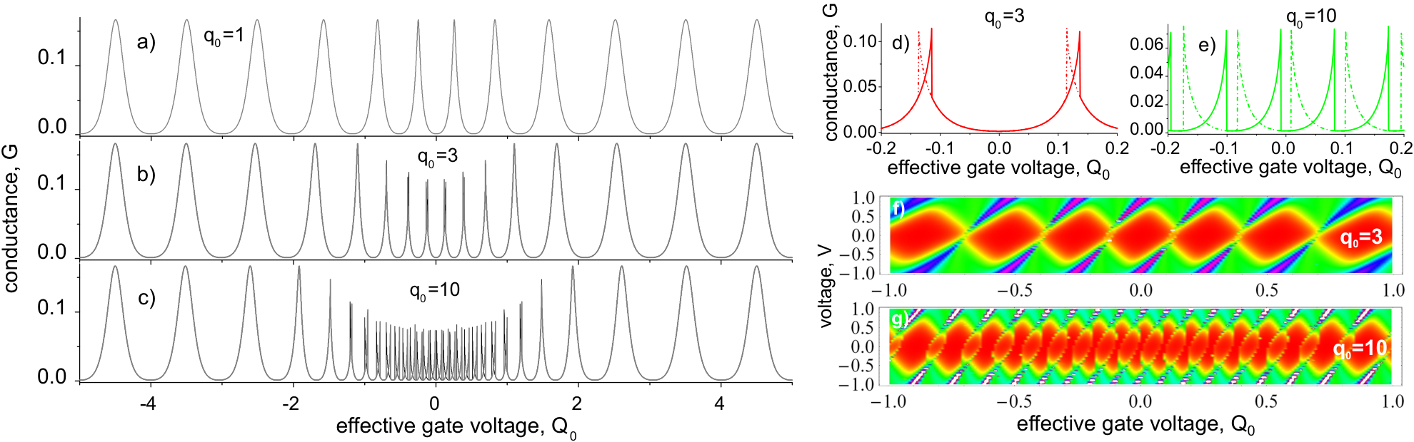
Now we consider small but finite values of switching voltage and investigate the correlation of the conductance peaks and polarization evolution with parameter . For parameter the conductance peaks do not merge, however they deform approaching the point . This is related to the switching of polarisation with , see Fig. 4.
For the conductance shows the pronounced memory effect (hysteresis), Fig. 3. The positions of the jumps in the conductance correspond to the divergences of . [15] The amplitude of the conductance peaks in this regime is suppressed for . The evolution of memory effect in the conductance with parameter is shown in Fig. 3. The conductance has similar behavior for and for its behavior coincide with conductance behavior for . Thus, the transport properties of SET are periodic in with the period . However, this statement is approximate: it is valid for small values of switching voltage and a negligible parameter only.
III.1.2 Ferroelectric with large switching field: . Breaking and condensation of conductance peaks.
For large switching field, , the picture is more complicated. The conductance is not a periodic function of parameter any more. Instead, some interesting effects related to the breaking and condensation of conductance peaks appear.
The closest peaks to are not only shifted but also reshaped and finally break at the critical values of parameter , Fig. 5. We classify the conductance peaks by their original positions at when they located at half-integer . We call peaks located at as the first pair of peaks, while peaks sitting at – the second pair of peaks. The first pair of conductance peaks breaks at , the second pair breaks at , Fig. 5. Increasing parameter the memory-dependent conductance peaks slowly regroup around , some of them even “collide” with each other, Fig. 5(d). We call this system behavior the conductance peak condensation.
We introduce the quantity . In the vicinity of zero voltage . For voltages we find . The relation between the grain charge and the grain potential has the form . The position of conductance peaks can be approximately evaluated using the following relation
| (7) |
In the vicinity of the distance between peaks reduces from to . For the interpeak distance becomes .
Now we focus on the polarization dependence of parameters and and their correlation with features in the conductance peaks. As follows in Fig. 5(e)-(h) the polarization also shows the memory effect similar to the conductance. In Fig. 5(g) one can see a number of hysteresis loops; their edges exactly correspond to features in the conductance; the number of the hysteresis loops corresponds to the number of conductance peaks broken and “condensed” near . At first glance the sharp changes in the polarization in Fig. 5 contradict the chosen parameter that makes the polarization a smooth function, Eq. (1). However, the features are related to the quantization of the excess charge on the grain of SET and not to the parameter .
In the vicinity of the ground state of the SET is described by Eqs. (33), (34) and (35). These equations provide the criterion for hysteresis appearance
| (8) |
The hysteresis appears first for peaks in the vicinity of where is large. At large the hysteresis disappears since . Similar to step-like polarization behavior the hysteresis disappears with increasing temperature.
In Fig. 6 we investigate the SET with large switching voltage, . Qualitatively the conductance behaviour is similar to the case of except the fact that more conductance peaks are involved in the memory effect for similar values of . Figure 6 shows the evolution of conductance with parameter . The density plots for conductance show a complicated structure, strongly nonperiodic in unlike the SET without ferroelectricity.
Analysing numerical data we conclude that conductance peaks condensation appears for the following gate voltages: or , where is the maximum grain potential. At zero temperature, , the maximum grain potential . The number of condensed peaks is approximately equal to the maximum polarization charge that ferroelectric can induce on the grain, .
III.1.3 Temperature dependence of the memory effect
The important question is the temperature dependence of the memory effect. According to Eq. (5) the width of the conductance peaks in SET without ferroelectricity is approximately proportional to the temperature. Similar effect can be seen with ferroelectric located in the gate capacitor, see Fig. 7(a). Moreover, it follows that there is a pronounced temperature dependence of the critical where the first, second etc… peaks undergo the bifurcation and acquire the memory dependence. The graphs of are shown in the inset of Fig. 7(c).
III.1.4 Influence of finite linear term in Eq. (1)

The presence of the linear term in Eq. (1) for polarization is strongly influence the conductance of SET, Fig. 7(b). Generally, finite leads to the renormalization of : . Finite causes the hysteresis behavior of all peaks at small enough temperature. The presence of small shifts the conductance peaks and reduces their amplitudes, while the larger changes the critical values of parameter where the corresponding conductance peaks undergo the bifurcation and acquire the memory dependence. Figure 7(d) shows that the presence of finite suppresses . There is a bifurcation point where all merge and reach zero. The behavior of conductance for is very different from its behaviour for . This is related to the fact that all are zero above therefore all the conductance peaks for any value of parameter have the hysteresis, Fig. 8.

The critical can be found analytically. We find corresponding to an ambiguous solution for the ferroelectric polarization in the limit using the self-consistency equation , Appendix A. Differentiating in voltage we find
| (9) |
where and denotes the average potential of SET without ferroelectric in the gate capacitor. The ambiguity in the solution of results in the appearance of singularity in its derivative. According to Eq. (9) the derivative becomes singular at some points if
| (10) |
According to the orthodox theory, the derivative of the average potential approaches its maximum at the degeneracy points leading to
| (11) |
Another effect due to the presence of finite is the renormalization of the distances between the conductance peaks for away from zero. For zero temperature the distances between peaks are reduced by a factor of .
III.1.5 Giant hysteresis memory-loop in the absence of hysteresis ().

Above we showed that ferroelectricity drives the memory effect. Here we show that it can be “giant”. This is so if the effective charge “induced” by the ferroelectric at the grain is large enough, for example , Fig. 9. We mention that we still use such that the hysteresis in is absent, Eq. (1). However, has a large hysteresis. Each small step in curve in Fig. 9(b) corresponds to the change of the grain charge by the charge quantum. This large Coulomb blockage hysteresis is further increased for . This giant hysteresis memory-loop has potential for applications in memory devices.
This effect can be thought of as an extreme case of “peak condensation”. When enough peaks are “condensed”, the conductance behavior acquire the quasi-oscillatory character in the vicinity of . Physically, this corresponds to the situation when a small change in causes the number of electrons on the grain to be changed by one at the expense of the FE polarization. As a result of being a periodic function of the number of excess electrons on the grain the conductance changes little in this process. The same is true for the average potential.
Below we discuss the SET parameters and conditions to observe the effect of gigantic hysteresis loop. First, the width of the hysteresis loop is restricted by the gate capacitance meaning that it is beneficial to have a large , . Second, the switching voltage should be of the order of 1 for the polarization not to flip to fast with the change of . Third, the conductance peaks should start merging meaning that there should be enough number of them (large ) and their width should be sufficient (not too low temperatures, ).
III.2 Ferroelectric with finite hysteresis loop
Now we consider a ferroelectric with finite hysteresis in the polarization — the electric field dependence is given by Eq. (1). In general the state of FE depends on the whole history of its evolution, however here we consider only processes with monotonous change of FE polarization where the hysteresis-loop approximation is valid.
Figure 10 shows the conductance and polarization of ferroelectric with finite width hysteresis loop. Graphs (a), (b), and (d) compare SETs with voltages and , where for there is no memory effect in the conductance . As follows the intrinsic hysteresis in the FE polarization-voltage dependence increases the hysteresis in the conductance.
This behavior is predictable in comparison to the negligible-hysteresis case. The hysteresis in Eq. (1) is equivalent to the introduction of an additional polarization-induced charge on the grain, where charge is being dependent on the evolution of .
| (12) |
This additional charge vanishes in the limit , but even in this limit it causes further retardation of the FE polarization change with in the region around zero. Moreover, the intrinsic FE polarization causes broadening of the interval of where the state of the FE SET is not unique. This interval region is estimated as .
IV Discussion
Typical experimental parameters of SETs and ferroelectric materials were discussed in details in our paper 15.
IV.1 Influence of cotunneling
Above we discussed the SET with ferroelectric gate using the orthodox theory. Now we go beyond this theory and show how the finite junction conductances influence our results. In particular, we show that the next order corrections to the SET conductance and the island occupation number do not qualitatively change the system behavior, but rather introduce some quantitative corrections.
The orthodox theory assumes that the junction conductances are small compare to and takes into account only the lowest order processes in the tunneling matrix elements. In this section we use the results of [24] to calculate the second order corrections to the conductance and the first order correction to the electron mean occupation number on the island. The latter results in a corrected average island potential that is used in the self-consistency equation.
In this section we measure the resistance in quantum units .
In the theory of SET the second order corrections in tunneling conductance manifest themselves in reshaping conductance peaks and in fluctuations of the electron number on the island. For SET with ferroelectric gate the first effect remains, except the fact that the reshaping becomes more complicated in the vicinity of . However, the quantum charge fluctuations introduce a new effect — they reduce the polarization hysteresis loop. This phenomenon stems from the fact that additional fluctuations of the island charge allow the FE polarization to be switched more easily. However, this effect cannot eliminate the hysteresis completely because the charge fluctuations are suppressed outside the conductance peaks. The typical shifts in the polarization hysteresis due to quantum fluctuations are shown in Fig. 11.
IV.2 Memory effect devices
The presence of hysteresis in transport characteristics of ferroelectric SET has potential applications for memory devices. The memory bit is associated with particular direction of the ferroelectric polarization in the gate capacitor. The memory storage corresponds to the zero gate voltage (). For example, if we measure the conductance at fixed parameter in Fig. 10(d) it gives the direction of the polarization. This is the reading operation. The writing information (fixation of a particular polarization direction) can be performed by applying a large enough gate voltage ().
The stored information may be strongly influenced by the fabrication-dependent SET parameters such as and . For instance, a change in by half of the elementary charge would shift the conductance peaks by half a period, dramatically changing the relationships between conductances and island potentials for opposite FE polarization.
For memory application the VDF-TrFE ferroelectric can be used. [25] It has the Curie point above the room temperature. The polarization of this relaxor in the vicinity of room temperature is about mkmC/m2 producing the charge e for grain size. Moreover, the magnitude of VDF-TrFE polarization can be tuned varying the VDF concentration. The dielectric permittivity of this relaxor is rather small in the vicinity of room temperature, . Therefore this ferroelectric can not suppress the Coulomb blockade effect and the charging energy can be as high as . This allows the memory device to operate at room temperature. For memory device the FE thickness can be of order . Assuming that the distance between the grain and the leads is about we obtain a good relation between the gate capacitance and the leads capacitors. The switching field of this FE is about giving . Using above estimates one can see that the SET with VDF-TrFE ferroelectric has behavior similar to the one shown in Fig. 10. Therefore this system can be used for memory application.
However, utilizing the giant hysteresis memory loop described in Sec. III.1.5 can provide another configuration, which is less sensible to the SET parameters. As numerical calculation show (see Fig. 11), for large enough parameter , the island potential tends to “stick” to its maximum or minimum value at depending on the way it was set there. Thus, the island potential may serve as a reliable indicator of the ferroelectric polarization which can be directly measured using an auxiliary quantum dot. [26]
IV.3 Conclusions
We investigate electron transport properties of SET with FE insulator placed between the metallic grain and the gate electrode. The mutual influence of charged grain and the FE polarization leads to drastic changes in the SET transport. In particular:
- 1.
There is an ambiguity in the characteristics of SET with ferroelectric gate-capacitor originating from nonlinear mutual influence of electron at the metallic grain and the FE polarization. It appears even in the absence of hysteresis in the FE polarization.
- 2.
The state of SET is no longer periodic in the gate voltage (). In particular, the “condensation” of conductance peaks appears in the vicinity of . The range of where conductance peaks condensate depends weakly on the ferroelectric properties and other transistor parameters. For the peak condensation appears for gate voltages or , where is the maximum grain potential. At zero temperature, , the maximum potential is . The number of the condensed peaks is approximately equal to the maximum polarization charge that ferroelectric can induce on the grain: .
- 3.
The linear part of the ferroelectric polarization substantially influences the conductance behavior as a function of parameter . In particular, the finite leads to the reduction of conductance peaks and the distances between the peaks in the whole range of (not only for small ).
- 4.
A finite hysteresis loop of the FE polarization makes the distinction between forward and backward change of voltage more pronounced. A finite voltage is not needed for ambiguity in the SET state to appear.
Acknowledgements.
N.C. acknowledges for the hospitality Laboratoire de Physique Théorique, Toulouse and CNRS where this work was finalized and SIMTECH Program, New Centure of Superconductivity: Ideas, Materials and Technologies (grant No. 246937). S. F., A. K, were supported by Russian Scientific Foundation (Grant No. RNF 14-12-01185), N.C. by RFBR No. 13-02-0057, and I. B. was supported by NSF under Cooperative Agreement Award No. EEC-1160504, NSF Award No. DMR-1158666, and the NSF PREM Award.Appendix A Theory of Ferroelectric Single Electron Transistor
A.1 Self-consistent solution
In this section we show how the influence of ferroelectric polarization can be included into the theory of SET. We limit our consideration to the case of sufficiently slow ferroelectric response times compare to the electron tunneling time . The opposite limit is discussed in Ref. 15. We consider the steady-state solutions.
We use the following Hamiltonian to describe the SET
| (13) |
Here , denotes Hamiltonians for isolated right and left leads and the island respectively, is the tunneling Hamiltonian, and is the Coulomb energy of the form
| (14) |
is the effective charge. The notations for voltages and capacitances are similar to Fig. 1.
The Coulomb Hamiltonian in Eq. (14) treats the dielectric polarizations in the junctions as classical variables. Thus it can be easily generalized to the case of an additional FE polarization by adding the term
| (15) |
Equation (15) is valid for ”frozen” FE polarization, meaning that it is constant on the time-scales of tunneling. This limit is justified assuming that the slow polarization is defined by the mean field and is weakly influenced by the fast field fluctuations of the charge tunneling. To find a steady state of SET the equilibrium FE polarization must be taken constant for calculating the electron tunneling rate. This constant polarization yields an additional constant charge on the island
| (16) |
The Coulomb Hamiltonian in Eq. (15) coincide with the usual SET Hamiltonian if we introduce a new effective gate charge . Thus for a given FE polarization the steady state of the FE SET can be calculated using the theory of usual SET. On the other hand, the polarization of the FE by itself is determined by the mean electric field resulting from the microscopical tunneling dynamics. Therefore the complete steady-state solution for the FE SET is obtained when the equilibrium FE polarization and the tunneling dynamics are calculated self-consistently. [15]
A.2 First order theory
Here we discussed the first order perturbation theory in tunneling. For the FE induced charge we use the following expression
| (17) |
Here is the voltage across the gate junction. The average island potential that plays a key role in determining the FE polarization is a linear function of the average island occupation number
| (18) |
In the leading order the probability per unit time to change the island occupation number from to through the first junction is given by the Fermi golden rule
| (19) |
where is the Bose-function, [27] is the tunnelling bare resistance and denotes the free energy change with being the effective charge
| (20) |
The flow rates defined the probabilities to find excess electrons on the island through the detailed-balance equations
| (21) |
with boundary conditions . In their turn, probabilities are used to calculate the average occupation number and the average potential through Eq. (18). The last step is to solve the equations (17) and (18) together to obtain a self-consistent solution.
Knowing the FE induced charge , the current through the SET can be found
| (22) |
where all the rates are calculated with being the effective charge.
A.3 Higher order corrections
Here we consider next order corrections to the average occupation number and to the tunneling current. If corrections for SET without FE are known as a function of the effective charge , these corrections can be generalized for FE SET. Indeed, to solve the self-consistency Eqs. (17) and (18) we need to know the dependence of on for SET without ferroelectricity. If this dependence is known, it can be placed in Eq. (18) with the proper substitution for .
In the Sec. IV.1 we used the results of Ref. 24 for low temperatures, where it was shown that in the first order theory the occupation probabilities of only two neighboring states ( and excess electrons) significantly deviate from zero. The correction to the average occupation number is given by
| (23) |
where
| (24) |
are the lowest-order state occupation probabilities, , denotes junctions and is the digamma function.
Following Ref. 24 we introduce the generalized flaw rates to calculate the corrections to the tunneling current
| (25) | |||
| (26) |
where — the chemical potentials of the electrodes. Additionally,
| (27) |
We consider the case with or excess electrons occupying the island. To calculate the corrections for arbitrary voltages and FE polarization we shift the parameter by where
| (28) |
Therefore, in the following we assume that . The first-order tunneling current can be written as follows
| (29) |
The second-order contribution to the tunneling current is divided into three parts , where
| (30) |
| (31) | |||
| (32) |
where and the poles at are regularized as Cauchy’s principal values and their derivatives .
A.4 Choosing branches
The self-consistent solution of Eqs. (17) and (18) may not be unique leading to the hysteresis behavior discussed in this paper. Thus we encounter the problem of choosing branches. Here we explain the rules for selecting the solutions.
The self-consistent state is unique for the effective charge being away from the resonance and the linear part of the FE polarizability being sufficiently small. There are two situations: i) evolved from to the right and ii) from to the left. Over the course of evolution at some values of parameter the solution can become discontinuous. In this case we assume that the polarization “jumps” to the nearest available position. There is no ambiguity in choosing the new state, because the polarization always evolves monotonically and takes its maximum or minimum value depending on the direction of evolution.
A.5 Ground state of FE SET with step-like polarization
For calculating the ground state of the system all states are important. However, the hopping probability decreases exponentially with increasing the free energy of a state. Therefore we consider only few states which are the closest to the considered point. The number of these states depends on the parameter and the considered point. For only two states and are important for calculating for any . Increasing parameter leads to moving of energy intersection points to . For the situation is more complicated. In the vicinity of a lot of intersections of different energy branches occur and one has to take into account many different states. However, for large values of only two states of energy intersection points are important.
We consider the case when two states are enough to describe the system state and concentrate on the vicinity of the point with and . The average charge is give by the expression
| (33) |
where are the probabilities for the system to be in the state with and electrons on the grain. If only two states are present we find
| (34) | ||||
where and the parameter is approximately the area of the grain in contact with the ferroelectric. Averaging Eq. (3) we find the following relation
| (35) |
Equations (33) and (35) have always a single solution. Therefore there is no hysteresis in the system for and arbitrary . The conductivity of SET has maximum at . These maximums are located at point . The average potential at these points is .
For and there is no hysteresis. In the vicinity of the system shows the hysteresis and can not be described by two states. For , three states need to be taken into account in the vicinity of , see Fig. 3. For , five states , etc.
For the system probabilities with have the form
| (36) |
The average charge is give by the following expression
| (37) |
Solving Eqs. (37) and (35) we find the average potential . Figure 12 shows the dependence Eq. 37 (solid line) and Eq. 35 (dashed line) on for . In this figure the curves have three intersections at points meaning that the system has hysteresis. The asymptotic behavior of Eq. (37) for is the following
| (38) |
The value depends on temperature and decreases with increasing . At temperature it becomes smaller than . For temperature the hysteresis disappears. However, at high enough temperatures all states needs to be taken into account and the description with three states only () can be incorrect.
References
- [1] M. Dawber, I. Szafraniak, M. Alexe, and J. Scott, J. Phys. C 15, L667 (2003).
- [2] C. Ahn, K. Rabe, and J.-M. Triscone, Science 303, 488 (2004).
- [3] M. Dawber, K. M. Rabe, and J. F. Scott, Rev. Mod. Phys. 77, 1083 (2005).
- [4] L. Wang, J. Yu, Y. Wang, G. Peng, F. Liu, and J. Gao, J. of Appl. Phys. 101, 104505 (2007).
- [5] Y.-J. Zhang, T.-L. Ren, and L.-T. Liu, Integrated Ferroelectrics 95, 199 (2007).
- [6] J. F. Scott, Science 315, 954 (2007).
- [7] P. Maksymovych, S. Jesse, P. Yu, R. Ramesh, A. P. Baddorf, and S. V. Kalinin, Science 324, 1421 (2009).
- [8] Y.-H. Chu, L. W. Martin, M. B. Holcomb, M. Gajek, S.-J. Han, Q. He, N. Balke, C.-H. Yang, D. Lee, W. Hu, Q. Zhan, P.-L. Yang, A. Fraile-Rodriguez, A. Scholl, S. X. Wang, and R. Ramesh, Nature Materials 7, 478 (2008).
- [9] W. Lee, H. Han, A. Lotnyk, M. A. Schubert, S. Senz, M. Alexe, D. Hesse, S. Baik, and U. Gösele, Nature Nanotechnology 3, 402 (2008).
- [10] S. V. Kalinin, A. N. Morozovska, L. Q. Chen, and B. J. Rodriguez, Rep. Prog. Phys. 73, 056502 (2010).
- [11] J. Sinsheimer, S. J. Callori, B. Bein, Y. Benkara, J. Daley, J. Coraor, D. Su, P. W. Stephens, and M. Dawber, Phys. Rev. Lett. 109, 167601 (2012).
- [12] S. J. Callori, J. Gabel, D. Su, J. Sinsheimer, M. V. Fernandez-Serra, and M. Dawber, Phys. Rev. Lett. 109, 067601 (2012).
- [13] N. Ortega, A. Kumar, J. Scott, D. B. Chrisey, M. Tomazawa, S. Kumari, D. Diestra, and R. Katiyar, J. Phys. C 24, 445901 (2012).
- [14] A. Chanthbouala, V. Garcia, R. O. Cherifi, K. Bouzehouane, S. Fusil, X. Moya, S. Xavier, H. Yamada, C. Deranlot, N. D. Mathur, M. Bibes, A. Barthélémy, and J. Grollier, Nature Materials 11, 860 (2012).
- [15] S. A. Fedorov, A. E. Korolkov, N. M. Chtchelkatchev, O. G. Udalov, and I. S. Beloborodov, Phys. Rev. B 89, 155410 (2014).
- [16] A. D. Armour, M. P. Blencowe, and Y. Zhang, Phys. Rev. B 69, 125313 (2004).
- [17] N. Nishiguchi, Phys. Rev. B 78, 085407 (2008).
- [18] A. N. Korotkov, Phys. Rev. B 49, 16518 (1994).
- [19] D. Averin and K. Likharev, Mesoscopic phenomena in solids 30, 173 (1991).
- [20] D. V. Averin, A. N. Korotkov, and K. K. Likharev, Phys. Rev. B 44, 6199 (1991).
- [21] M. Devoret and H. Grabert, Single Charge Tunneling, Vol. 264 (New York, Plenum, 1992).
- [22] C. Wasshuber, Computational single-electronics (Springer, 2001).
- [23] The jumps in the conductance and polarization in Fig. 3 for are also related to the memory effect instability but with rather thin hysteresis loop .
- [24] J. König, H. Schoeller, and G. Schön, Phys. Rev. Lett. 78, 4482 (1997).
- [25] T. Yamada and T. Kitayama, J. Appl. Phys. 52 (1981).
- [26] C. F. F. H. Niels Ubbelohde, Christian Fricke and R. J. Haug, Nat Commun 3, 612 (2012).
- [27] N. M. Chtchelkatchev, A. Glatz, and I. S. Beloborodov, Phys. Rev. B 88, 125130 (2013).