Non-Markovian electron dynamics in nanostructures coupled to dissipative contacts
Abstract
In quasiballistic semiconductor nanostructures, carrier exchange between the active region and dissipative contacts is the mechanism that governs relaxation. In this paper, we present a theoretical treatment of transient quantum transport in quasiballistic semiconductor nanostructures, which is based on the open system theory and valid on timescales much longer than the characteristic relaxation time in the contacts. The approach relies on a model interaction between the current-limiting active region and the contacts, given in the scattering-state basis. We derive a non-Markovian master equation for the irreversible evolution of the active region’s many-body statistical operator by coarse-graining the exact dynamical map over the contact relaxation time. In order to obtain the response quantities of a nanostructure under bias, such as the potential and the charge and current densities, the non-Markovian master equation must be solved numerically together with the Schrödinger, Poisson, and continuity equations. We discuss how to numerically solve this coupled system of equations and illustrate the approach on the example of a silicon nin diode.
I Introduction
In nanoscale, quasiballistic electronic systems under bias, the process of relaxation towards a nonequilibrium steady state cannot be attributed to scattering, because these structures are small compared to the carrier mean free path [2, 3]. Rather, the active region of a nanostructure is an open quantum-mechanical system that exchanges particles and information with the dissipative reservoirs of charge, usually referred to as contacts [4, 5]. While qualitatively clear, a quantitative description of the irreversible evolution of the electronic system in this regime, where dissipation in the contacts coupled with the carrier exchange between the active region and contacts is the mechanism governing relaxation, is very challenging [6, 7, 8].
In this paper, we present a theoretical treatment of the transient-regime evolution of the electronic system in a two-terminal ballistic nanostructure coupled to dissipative contacts and illustrate it on the example of a semiconductor nin diode. The approach is rooted in the open system theory [9, 10]. We start from the closed-system, Hamiltonian dynamics of the many-body statistical operator for the ballistic active region and the dissipative contacts together, with a model interaction describing the injection of electrons into the active region. The model interaction Hamiltonian differs from those typically employed [11, 12]: it is specifically constructed to conserve current during the process of carrier injection from/into the contacts, and its matrix elements are readily calculated from the single-particle transmission problem for structures with and without resonances alike (Sec. II). As is commonly done, we trace out the contact degrees of freedom and obtain the exact non-Markovian dynamical map that describes the evolution of the active region’s statistical operator. However, while exact, this map is not useful in practical calculations. In order to obtain a tractable theoretical approach, we employ the fact that relaxation in the contacts of a nanostructure typically occurs on the shortest timescales in the whole system. We assume that the contacts are highly doped, so the fastest scattering mechanism is electron-electron scattering [13, 14, 15]. Within the momentum relaxation time, the contacts adjust themselves to the new level of current flowing through the structure. The momentum relaxation time is virtually instantaneous from the standpoint of the nanostructure as a whole; if we are not to look into the microscopic details of relaxation in the contacts, but want to include their effect on the overall evolution of the nanostructure, the momentum relaxation time can be considered the shortest meaningfully resolvable time. Therefore, we coarse-grain the evolution over the contact momentum relaxation time and obtain a dynamical map that is piecewise Markovian but globally a non-Markovian, completely positive map (Sec. III). We present a numerical algorithm for the calculation of relevant response quantities such as the charge density, potential, and current density based on the presented model, and illustrate the approach with a calculation of the response of a realistic semiconductor nin diode in Sec. IV.
II Interaction between the active region and the contacts
It has been well-established that the active region of a nanostructure is an open quantum-mechanical system [16, 17]. Usually, the effect of openness is treated through open boundary conditions; examples of such treatment are the explicit source terms in the density matrix [18] or Wigner function formalisms [16, 19]. Alternatively, a dynamical quantity is ascribed to the coupling between the active region and the contact: in the popular tight-binding variant of the nonequilibrium Green’s function formalism, pioneered by Datta [20], the active region-contact coupling is described through a special self-energy term. In the Meir-Wingreen [11, 12] approach and its derivatives, one employs a coupling Hamiltonian between the contacts and the active region, but no general recipe is available for the derivation of the Hamiltonian matrix elements. Also, this approach has so far been applied only when the active region supports a small number of discrete states, so the model has little practical value for structures with no resonances, such as an nin diode, or to account for the continuum states in structures with mixed spectrum, such as a double-barrier tunneling structure (also known as the resonant-tunneling diode). We present an alternative interaction Hamiltonian that does nor require that a structure a priori possesses resonances, and whose matrix elements are straightforwardly derived from the single particle transmission problem.

Consider a generic two-terminal nanostructure under bias (Fig. 1). For every energy above the bottom of the left contact, the active region’s single particle Hamiltonian has two eigenfunctions, a forward () and a backward () propagating state, that can be found by (in general numerically) solving the single-particle Schrödinger equation for a given potential profile in the active region. Associated with () in the active region are the creation and destruction operators and ( and ), so the active region many-body Hamiltonian is
| (1) |
Spin is disregarded, and . In the case of ballistic injection through the open boundaries, each state is naturally coupled with the injected states from the left contact. For , the coupling is with from the right contact (, where is the applied bias). To model this coupling via a hopping-type interaction, we can write quite generally (see Fig. 1)
| (2) |
() and () create (destroy) an electron with a wavevector in the left and in the right contact, respectively. The hopping coefficients and are proportional to the current carried by each mode, i.e.
| (3) |
where is the transmission coefficient of mode . can be written in terms of the scattering-state injection amplitude [22].
III The transport master equation
In general, the dynamics of a nanostructure’s active region is non-unitary and non-Markovian (i.e., memory effects are important, meaning that the system remembers how it got to a certain state and its future direction of evolution depends not only on the state it is currently in, but also on how it got to that state to begin with). A non-Markovian, non-unitary map that would describe the active region in a ballistic nanostructure in the presence of contacts can be derived by tracing our the contact degrees of freedom from the unitary evolution of the closed ”active region and contacts” system. A general form of the non-Markovian evolution of the active region statistical operator is given by , where map is of the form
| (4) |
Here, is the generator of the map . In general, it is impossible to obtain exactly. If one is interested in retaining the non-Markovian nature of (4), typically an expansion up to the second or fourth order in the interaction is undertaken [10]. On the other hand, a Markovian approximation to the exact dynamics can quite generally be obtained in the weak-coupling limit. This limit has been used previously by several authors [23, 24] to derive Markovian rate equations for tunneling structures in the resonant-level model, although the weak-coupling approximation is not generally applicable to nanostructures [23].
However, here we point out the Markovian approximation to the long-time evolution of nanostructures can be justified more broadly, by employing the approximation of a memoryless environment for the contacts. Basically, electron-electron scattering in the highly doped contacts of semiconductor devices ensures that the carrier distribution snaps into a drifted Fermi-Dirac distribution [13] within the energy-relaxation time femtoseconds [14, 15] (the actual value depends on the doping density and temperature). This time is very short with respect to the typical response times of these devices, which is on the timescales of ps (”AR” stands for the active region), so on these timescales contacts can be considered memoryless. For low-dimensional nanostructures, fabricated on a high-mobility two-dimensional electron gas (2DEG) and operating at low temperatures, phonons are frozen so the energy relaxation in the contacts is also governed by the inelastic electron-electron scattering [25, 26]. The ratio is not as small as in devices, but is still less than unity.
To practically obtain the Markovian approximation due to an environment that loses memory after a time , we use the coarse-graining procedure: we can partition the time axis into intervals of length , , so the environment interacts with the system in exactly the same way during each interval [27],
| (5) |
where is the averaged value of the map’s generator over any interval ( is reset at each ). If the coarse-graining time is short enough, then the short-time expansion of can be used to perform the coarse-graining [21], so we finally arrive at the desired Markovian kinetic equation
| (6) |
where is an effective system Liouvillian, containing the noninteracting-system Liouvillian and a correction due to the interaction [ denotes the partial average with respect to the initial environmental state ]. The matrix elements of superoperator , in a basis in the system’s Liouville space (Liouville space is basically a tensor square of the Hilbert space), are determined from the matrix elements of the interaction Hamiltonian:
| (7) | |||||
where are the eigenvalues of the initial environment statistical operator . contains essential information on the directions of coherence loss. Strictly speaking, the above coarse-graining procedure holds if
| (8) |
Since the interaction Hamiltonian is linear in the contact creation and destruction operators, and we can approximate that each contact snaps back to a ”drifted” grand-canonical statistical operator, we have . This means that , and also leaves us with only the first three terms in Eq. (7) for to calculate. It can be shown [21] that each term in is a sum of independent contributions over individual modes [] that attack only single-particle states with a given . The same holds for . Consequently, in reality we have a multitude of two-level problems, one for each state , where the two levels are a particle being in (”+”) and a particle being absent from (”-”). Each such 2-level problem is cast on its own 4-dimensional Liouville space, with being the reduced statistical operator that describes the occupation of . According to (6),
| (9) |
where
and
| (19) |
The rows/columns are ordered as . Clearly, off-diagonal elements and decay as and reach zero in the steady state. The two equations for and are actually one and the same, and either one yields
| (20a) | |||
| where is the distribution function for the active region. An analogous relationship holds for the backward-propagating states: | |||
| (20b) | |||
Equations (20) may at first glance appear to be Markovian in form, but they are generally not, as we will discuss in the next section. However, if we are in the low-bias regime and assume that: (1) the potential and thus the scattering states, transmission coefficients, and the coupling strengths are virtually constant throughout the transient, and (2) the current density is low, so any changes to the contact distribution functions that result from a current flow can also be neglected, then evolution (20) will indeed be Markovian [21]. In fact, we can solve the above equations analytically in the limit of low bias and low current densities. In that case, the contact distribution functions are nearly constant, and the solution to Eqs. (24) can be found as
| (21) | |||||
As expected, the steady-state values of the distribution functions are the contact distribution functions
| (22) |
A detailed discussion of the relationship of the model with the Landauer-Büttiker formalism can be found in [21].
IV Example: Transient in an nin diode
As the current starts to flow through the structure, the contact distribution functions quickly adjust to accommodate the current flow. A good approximation for the distribution function in bulklike contacts in which electron-electron scattering is the most efficient mechanism is the drifted Fermi-Dirac distribution function
| (23) |
where , the drift wave vector, depends on the total current density flowing through the structure as . is the effective mass in the direction of current flow, and is the contact carrier density. changes during the transient and brings about non-Markovian character to Eqs. (24):
| (24) | |||||
where it should be understood that changes with time.
As the transient progresses, the current and the charge density in the structure change, which in turn changes the potential profile, the scattering states available to electrons, the transmission coefficients, and, to a small degree, the interaction matrix elements , as well as the aforementioned contact distribution functions. Therefore, all these quantities have to be carefully updated during the simulation.

Equations (24) must in general be solved numerically. A flowchart of the numerical algorithm is presented in Fig. 2. Upon the application of bias to the contact, but before the current starts to flow (), we solve the Schrödinger and Poisson equations with equilibrium initial distribution functions . At this point current continuity between the contacts and device is not necessary and (). We then proceed to the next time step, with non-zero current, and solve first the Schrödinger equation using the potential from the previous time step. Using the previous value for , we update the distribution functions at the new time step and calculate the current and charge densities, then find the current density due to the change in the device charge density, iterate for a new until the current density in the contacts is equal to the sum of the current density in the device and the current density due to the change in the device charge density. In each new iteration, we use a that is formed as a weighted sum of ’s from the current and previous iterations. When the current and are self-consistently obtained, we use the newly obtained device charge density in the Poisson equation to obtain a new guess for the potential, and repeat until the potential converges (using the globally convergent Newton’s method [28] with a semiclassical Jacobian [29, 30]). We repeat for all time steps until a steady state is reached.
There are several nontrivial numerical considerations. One is the ability to achieve a high enough density of scattering states to properly represent physical quantities such as the charge and current densities or the potential profile. We are trying to capture a continuum of scattering states, which at first glance might seem doable by indiscriminately increasing the density of ’s by choosing larger and larger simulation domains. Unfortunately, this brute-numerical-force approach does not work; what does work instead is generating a ”smart” discrete set of scattering states by first solving the Schrödinger equation in the simulation domain with the condition that the first derivative be zero at the boundaries, and then projecting these states onto the forward and backward moving scattering states. Details of this discretization of the scattering state continuum can be found in [30].
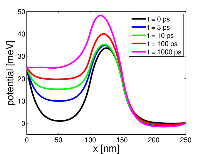
A related question is how to populate a small set of bound states that can emerge in a biased nanostructure (e.g. note the potential pocket on the left-hand-side of Fig. 3a at times below 100 ps). Those states are in reality filled by electron-electron and electron-phonon scattering, essentially the same mechanisms as in the contacts. Since we are not treating scattering explicitly in this approach, we populate the bound states according to the Fermi level in the nearest contact. More detail on the finer points of the numerical simulation can be found in [22].
Figures 3 and 4 depict the potential, charge density, and current density for a single ellipsoidal valley in an nin silicon diode at room temperature. The left and right contacts are doped to cm-3, whereas the middle region is intrinsic (undoped). The momentum relaxation time in the contacts is taken to be 120 fs, based on the textbook mobility values for the above doping density. Note that the characteristic response time of the current is of order hundreds of picoseconds, so three orders of magnitude greater than the contact relaxation time. The transient duration is long because of the relatively weak coupling between the active region and the contacts; the transient duration can be thought of as the inverse of a typical among the ’s participating in the current flow.


V Conclusion
We presented a theoretical treatment of the transient-regime evolution of an electronic system in a two-terminal ballistic nanostructure coupled to dissipative contacts. The approach is rooted in the open system theory and is based on two key ingredients: (1) A model interaction Hamiltonian between the active region and the contacts, constructed specifically to conserve current during the process of carrier injection from/into the contacts, whose matrix elements are readily calculated from the single-particle transmission problem for structures with and without resonances alike. (2) In the absence of scattering in the active region, it is the rapid energy relaxation in the contacts (due to electron-phonon or, in good, highly-doped contacts, due to electron-electron scattering) that is the indirect source of irreversibility in the evolution of the current-limiting active region, owing to the contact-active region coupling. We account for the influence of the rapid relaxation in the contacts by coarse graining the exact active region evolution over the contact momentum relaxation time. The resulting equations of motion for the distribution functions of the forward and backward propagating states in the active region, Eqs. (24), have non-Markovian character as they incorporate the time-varying contact distribution functions through the time-dependent drift-wavevector that depends on the instantaneous current flowing. In order to obtain the response quantities of a nanostructure under bias, such as the potential and the charge and current densities, the non-Markovian master equations must be solved numerically together with the Schrödinger, Poisson, and continuity equations. We presented an algorithm for the numerical solution of this coupled system of equations and illustrated the approach on the example of a silicon nin diode.
VI Acknowledgment
This work has been supported by the NSF, award ECCS-0547415.
References
- [2] M. Lundstrom, Fundamentals of Carrier Transport (Cambridge University Press, Cambridge, 2000).
- [3] D. K. Ferry and S. M. Goodnick, Transport in Nanostructures (Cambridge University Press, Cambridge, UK, 1997).
- [4] M. V. Fischetti, J. Appl. Phys. 83, 270–291 (1998).
- [5] M. V. Fischetti, Phys. Rev. B 59, 4901–4917 (1999).
- [6] D. K. Ferry, R. Akis, J. P. Bird, M. Elhassan, I. Knezevic, C. Prasad, and A. Shailos, J. Vac. Sci. Technol. B 21, 1891–1895 (2003).
- [7] G. Ferrari, N. Giacobbi, P. Bordone, A. Bertoni, and C. Jacoboni, Semicond. Sci. Tech. 19, S254–S256 (2004).
- [8] R. Gebauer and R. Car, Phys. Rev. Lett. 93, 160404 (2004).
- [9] R. Alicki and K. Lendi, Quantum Dynamical Semigroups and Applications, Lecture Notes in Physics, Vol. 286 (Springer-Verlag, Berlin, 1987).
- [10] H. P. Breuer and F. Petruccione, The Theory of Open Quantum Systems (Oxford University Press, Oxford, 2002).
- [11] Y. Meir and N. S. Wingreen, Phys. Rev. Lett. 68, 2512 (1992).
- [12] A. P. Jauho, N. S. Wingreen, and Y. Meir, Phys. Rev. B 50, 5528 (1994).
- [13] P. Lugli and D. K. Ferry, IEEE Trans. Electron Devices 32, 2431–2437 (1985).
- [14] M. A. Osman and D. K. Ferry, Phys. Rev. B 36, 6018 (1987).
- [15] A. M. Kriman, M. J. Kann, D. K. Ferry, and R. Joshi, Phys. Rev. Lett. 65, 1619–1622 (1990).
- [16] W. R. Frensley, Rev. Mod. Phys. 62, 745 (1990).
- [17] W. Pötz, J. Appl. Phys. 66, 2458 (1989).
- [18] R. Brunetti, C. Jacoboni, and F. Rossi, Phys. Rev. B 39, 10781 (1989).
- [19] M. Nedjalkov, H. Kosina, S. Selberherr, C. Ringhofer, and D. K. Ferry, Phys. Rev. B 70, 115319 (2004).
- [20] S. Datta and M. P. Anantram, Phys. Rev. B 45, 13761 (1992).
- [21] I. Knezevic, Phys. Rev. B 77, 125301 (2008).
- [22] B. Novakovic and I. Knezevic (2012), in preparation.
- [23] X. Q. Li, J. Y. Luo, Y. G. Yang, P. Cui, and Y. J. Yan, Phys. Rev. B 71, 205304 (2005).
- [24] J. N. Pedersen and A. Wacker, Phys. Rev. B 72, 195330 (2005).
- [25] B. L. Altshuler and A. G. Aronov, JETP Lett. 30, 514 (1979).
- [26] B. L. Altshuler and A. G. Aronov, Solid State Commun. 38, 11 (1981).
- [27] D. A. Lidar, Z. Bihary, and K. B. Whaley, Chem. Phys. 268, 35 (2001).
- [28] W. H. Press, S. A. Teukolsky, W. T. Vetterling, and B. P. Flannery, Fortran Numerical Recipes, Vol. 1, Numerical Recipes in Fortran 77: The Art of Scientific Computing, 2 edition (Cambridge University Press, New York, 1992).
- [29] R. Lake, G. Klimeck, R. C. Bowen, and D. Jovanovic, J. Appl. Phys. 81, 7845 (1997).
- [30] S. E. Laux, A. Kumar, and M. V. Fischetti, J. Appl. Phys. 95, 5545–5582 (2004).