Wannier-Stark states of graphene in strong electric field
Abstract
We find theoretically energy spectrum of a graphene monolayer in a strong constant electric field using a tight-binding model. Within a single band, we find quantized equidistant energy levels (Wannier-Stark ladder), separated by the Bloch frequency. Singular interband coupling results in mixing of the states of different bands and anticrossing of corresponding levels, which is described analytically near Dirac points and is related to the Pancharatnam-Berry phase. The rate of interband tunneling, which is proportional to the anticrossing gaps in the spectrum, is only inversely proportional to the tunneling distance, in a sharp contrast to conventional solids where this dependence is exponential. This singularity will have major consequences for graphene behavior in strong ultrafast optical fields, in particular, leading to non-adiabaticity of electron excitation dynamics.
I Introduction
Dynamics of an electron in periodic potential and external electric field is characterized by Bloch oscillations [1], which is a feature of the intraband electron dynamics, and Zener tunneling [2], which is related to interband coupling. The Bloch oscillations occur due to acceleration of an electron by electric field, which is described by the “acceleration theorem” in the reciprocal space [3], and subsequent Bragg reflections from the periodic lattice potential at the boundaries of the first Brillouin zone. The interference of the electron wave packet, following such periodic dynamics in the reciprocal space, results in Wannier-Stark (WS) localization of an electron in the coordinate space [3, 4]. These WS states within a given band are separated by the Bloch oscillation frequency [1] forming an equidistant WS ladder. The Bloch oscillations and the corresponding WS states have been observed experimentally in semiconductor superlattices [5, 6, 7, 8, 9]. Recently the Bloch oscillations were reportedto to play a major role in high harmonic generation by intense infrared [10] and terahertz [11] pulses in crystalline solids.
The external electric field not only modifies the intraband electron dynamics, which results in the formation of the WS states, but also introduces interband coupling of the states of different bands. Such coupling can be described in terms of the Zener tunneling resulting in finite widths of the WS levels (resonances) of individual bands [12, 13, 14, 15], or in terms of eigenstates of coupled Hamiltonian, which results in mixing of the corresponding WS states of different bands. The strongest mixing occurs in the resonance, when the energies of the WS levels of different bands are equal. As a function of electric field, at these points the levels exhibit anticrossing behavior. In time-dependent electric field, e.g., in the electric field of an optical pulse, passing of these anticrossings defines time-dependent electron dynamics. This can be described as an adiabatic formation of WS states of different bands with subsequent passage of the anticrossing points. Depending on relation between the anticrossing gap and the rate of change of electric field, the dynamics of this passage can be adiabatic or diabatic [16]. Such a description of electron dynamics in time-dependent electric field was successfully used for interpretation of experimental results on interaction of ultrashort intense optical pulses with dielectrics [17, 18].
Description of interaction of time-dependent electric field, e.g., optical pulse, with a solid in terms of the dynamics of passage of anticrossing points requires knowledge of both the positions of the anticrossing points and the magnitudes of the corresponding anticrossing gaps. These parameters depend on the band structure of the solid and on the strength of the interband coupling. Below we study the properties of the WS states of monolayer graphene with potential application to the description of the interaction of strong optical field with electrons in graphene.
Graphene monolayer [19, 20, 21] has a honeycomb two-dimensional crystal structure with unique energy dispersion relation. Namely, the low-energy excitations are gapless and are described by the Dirac relativistic massless equation with two Dirac cones. Another important feature of this relativistic energy dispersion is singularity of the interband dipole matrix element between the valence and conduction bands at the Dirac points. In this case, the corresponding interband coupling, introduced by an electric field, is strong near the discrete Dirac points.
Below in this article we show that, due to this property, the stationary Schrödinger equation in a constant electric field can be solved exactly within the nearest neighbor tight-binding model of graphene for the electric field in the rational crystallographic directions. Previously, the WS energy spectra of electrons on a honeycomb lattice were studied in Ref. [22] in the tight-binding approximation for both rational and irrational directions of the electric field. It was shown that for an electric field in a rational direction, there was the WS localization of the electron wave functions in the field directions while in the normal direction they were delocalized.
II Main Equations
The WS states of an electron in graphene are defined as electron states in periodic lattice potential of graphene and in constant external electric field. These can be found as solutions of the Schrödinger equation,
| (1) |
where is a single-particle Hamiltonian, which has the form
| (2) |
Here is a single electron Hamiltonian of graphene, which determines the electron dynamics in periodic lattice potential of graphene, is a 2d vector, is unit charge, and is the external constant electric field with the magnitude and the direction, determined by angle relative to the axis - see Fig. 1(b).
We describe the electron states in graphene within the nearest neighbor tight-binding model [23, 24, 25, 26] with the tight-binding coupling between the sites of two sublattices ”A” and ”B” of graphene crystal structure - see Fig. 1(a). Such a model describes both the conduction and valence bands of graphene and captures the properties of the Dirac points. In the reciprocal space, the tight-binding Hamiltonian can be represented by a matrix of the form [23, 24]
| (3) |
where eV is the hopping integral and
| (4) |
Here is a lattice constant. The energy spectrum of Hamiltonian consists of conduction band ( or anti-bonding band) and valence bands ( or bonding band) with the energy dispersion (conduction band) and (valence band). This energy dispersion is shown in Fig. 1(c). It consists of two inequivalent sets of three Dirac points (and cones) and . The corresponding wave functions of the conduction and valence bands are, respectively,
| (5) |
and
| (6) |
where we denote . The wave functions and have two components corresponding to two sublattices A and B.


Taking the eigenfunctions and of Hamiltonian as the basis, we express the general solution of Schrödinger equation (1) in the form
| (7) |
Expansion coefficients and satisfy the following eigenvalue equations (see the Appendix).
| (8) |
| (9) |
where is the dipole matrix element between the conduction and valence band states with the wave vector , i.e.,
| (10) |
Substituting conduction and valence band wave functions (5) and (6) into Eq. (10), we obtain the following expressions for the interband dipole matrix elements:
| (11) |
and
| (12) |
A solution, and , of Eqs. (8)-(9) should satisfy periodic boundary condition in the reciprocal space with the periodicity of the reciprocal lattice. From this condition, we obtain the WS energy spectrum – Sec. III below.
Equations (8)-(9) constitute a system of the first order differential equations, where a constant electric field introduces both interband and intraband coupling of the electron states. The interband coupling is realized only between the states with the same wave vector, while the intraband coupling occurs only between the states laying in the reciprocal space along a trajectory determined by the direction of electric field. These trajectories can be identified by considering electron dynamics in a reciprocal space in a constant electric field. If an electron is initially at some point of the reciprocal space and a constant electric field is applied, then this electron will drift along the direction of the electric field following the acceleration theorem, , experiencing Bragg scattering at the boundaries of the Brillouin zone. Then the corresponding electron trajectory in the reciprocal space determines the line of coupled states.
The intraband-coupled states can be described by considering the states either in the first Brillouin zone only or in the entire reciprocal space. In either case, the equivalence of the points connected by a vector of reciprocal lattice should be taken into account. Such equivalence determines the periodic boundary conditions in the reciprocal space, from which the energy spectrum can be obtained.
First, we assume that the electric field is parallel to the axis. In this case, the lines of coupled states are also parallel to the axis and are parametrized by the component of the wave vector, . In Fig. 2 the states coupled by this electric field are shown in the first Brillouin zone [Fig. 2(a)] and in the extended reciprocal space [Fig. 2(b)]. In the first Brillouin zone, we need to take into account equivalence of the points connected by a vector of the reciprocal lattice, e.g., points and are equivalent. In Fig. 2, two sets of coupled states (lines) corresponding to different values of are shown. If then the typical line of coupled states is shown by the blue solid line in Fig. 2. The solid blue points at the ends of the line are coupled by a vector of reciprocal lattice, which determines the periodic boundary conditions for the wave functions and , i.e., and . From these conditions, the energy spectrum is obtained.
If , then the line of coupled states in the first Brillouin zone consists of two line segments, which are shown by red solid lines in Fig. 2(a). These line segments have two sets of equivalent points: solid red points and open red points. The points in each set are connected by the corresponding vector of the reciprocal lattice.
In the extended reciprocal space, a part of which is shown in Fig. 2(b), the lines, which describe the coupled states, are straight lines for both and . For the case , the line of coupled states is located in two Brillouin zones – see Fig. 2(b). For both the red and blue lines, the end points are connected by the same vector of reciprocal lattice, , which makes the end points equivalent and introduces periodic boundary conditions for the system of equations (8)-(9).
III Results and Discussion
III.1 Wannier-Stark levels of a single band
Without interband coupling, i.e., for , Eqs. (8)-(9) become decoupled. For a single band, e.g., valence band, Eq. (8) becomes
| (13) |
where the electric field is parallel to the axis. Solution of the first order differential equation (13) has the form
| (14) | |||||
where we introduced a notation, . From the periodicity of the wave function, , we obtain the WS energy spectrum as
| (15) |
where is an integer, and the band offset, , is
| (16) |
The Bloch frequency in Eq. (15) is defined as
| (17) |
The energy spectrum of Eq. (15) forms the WS ladder with equidistant energy levels.
For the conduction band, the energy spectrum has a similar form,
| (18) |
with the corresponding band offset
| (19) |
For the tight-binding model, introduced above, there is a relation . The wave functions of the WS levels of the conduction band are
| (20) | |||||
In the coordinate space, the WS levels are localized and the integer index determines the center of localization.
III.2 Wannier-Stark states of two-band model: Analytical results
III.2.1 Energy spectrum
The interband coupling, determined by dipole matrix elements , has a strong dependence on wave vector . Near the Dirac points ( and points in Fig. 1), the dipole matrix elements have sharp peaks. Dependence of the dipole matrix element, , on the wave vector, , for different values of is shown in Fig. 3. The Dirac point is at , i.e. it corresponds to and . Away from the Dirac point, i.e., when [see Fig. 3(a)], the dipole matrix element, , has a broad maximum near . With increasing , the maximum becomes more pronounced. Near the Dirac point [see, e.g., the case of in Fig. 3(b)], the dipole matrix element, , has a sharp peak at . Near this peak, the dipole matrix element, , behaves as
| (21) |
where and . Thus, for a given , the maximum value of the dipole matrix element is , diverging at .

Although the shape of as a function of depends on the value of the component of the wave vector, , the net interband coupling, which can be characterized by the integral
| (22) | |||||
which does not depend on . The interband transitional dipole, , is determined by the Pancharatnam-Berry phase, [27, 28], as characteristic of dielectric responses of crystalline solids [29, 30, 31]. This also suggests that Eq. (22), as defined by the symmetry of the system, is more general than the tight-binding model, in which the specific calculations are made.
A strong dependence of the dipole matrix element on near the Dirac point, which is illustrated in Fig. 3 and is supported by Eq. (21), can be approximated by the -function, i.e.
| (23) |
Here strength of the -function is determined by the condition that the net dipole coupling in Eqs. (22) and (23) is the same, which yields .
For the -function profile of the dipole matrix elements, the system of equations (8)-(9) can be solved analytically. Such solution can be obtained as follows. We are looking for a solution of the system of equation (8)-(9) within a line segment with the periodical boundary conditions at the ends. (Here, it is convenient to consider interval and not interval introduced before.) The dipole matrix element is non-zero only at . Then, for and , there is no interband coupling between the valence and conduction bands. Within these intervals, the general solution of the system (8)-(9) acquires the form for ,
| (24) | |||||
| (25) | |||||
and the same form with different coefficients for ,
| (26) | |||||
| (27) | |||||
where , , , and are constants.
At point , the -function dependence of dipole matrix element (23) introduces the following relation between the values of the wave function at and :
| (28) | |||
| (29) |
Thus, the -function coupling results in rotation of a pseudospin, which is associated with two components of the wave function, by a finite angle .
Substituting expressions (24)-(27) into relations (28)-(29) and taking into account the periodic boundary conditions, we obtain an equation for the energy spectrum of the WS states,
| (30) |
where we took into account relation , which is valid within the tight-binding model introduced above. The solution of Eq. (30) is parametrized by an integer number ; it describes the WS-state energies and has the form
| (31) |
Here the signs correspond to the the conduction () and valence () bands, respectively.
It is convenient to rewrite Eq. (31) in dimensionless energy variables normalized to the Bloch frequency, and as
| (32) |

The corresponding dimensionless energy spectrum is shown in Fig. 4(a). The anticrossing points of the energy levels can be clearly identified. These points are the anticrossings of the WS ladders of the conduction and valence bands – see Fig. 4(b) – corresponding to the interband Zener tunneling [2]. This interband coupling (Zener tunneling) makes the initial WS states of isolated bands to be non-stationary (metastable) but causes the formation of new, stationary states of the coupled bands that we consider in this article.
The anticrossing points can be labeled by an integer number . which has meaning of the number of unit cells through which the Zener tunneling occurs. In dimensionless variables, the positions of the anticrossing points are
| (33) |
or, in terms of the electric field, the anticrossing points are at
| (34) |
The positions of the anticrossing points can be also estimated from the expressions (15), (18) for the energies of the WS states of uncoupled conduction and valence bands. For uncoupled bands, the anticrossing points are determined by an equation , from which one can derive the positions of the anticrossing points at
| (35) |
where . Comparing exact expression (34) with approximation (35), we can conclude that the interband coupling for in the vicinity of the Dirac point eliminates field-induced renormalization of an anticrossing position,
| (36) |
At the same time, for far from the Dirac point, the interband coupling shifts the anticrossing points to the higher values of electric field similar to ordinary 3d solids [16] (see also below in Sec. III.3).
In the dimensionless units, the anticrossing gaps are the same for all anticrossing points [cf. Fig. 4(a)]. The value of the dimensionless gap, , can be found as the difference between the corresponding energy levels, , calculated at a point . This way, we find
| (37) |
In the original units, the anticrossing gap corresponding to the anticrossing point with index [see Eq. (33)] takes the form
| (38) |
Such weak dependence of the anticrossing gap on index is a unique feature of graphene’s unconventional relativistic-like low-energy dispersion relation. This behavior is quite different from that of conventional solids, e.g., dielectrics, for which the anticrossing gaps are exponentially decreasing with .
The physical meaning of is that the value of is the distance between the localized WS states of the conduction and valence bands. Then, the anticrossing gap with index is determined by a coupling of the WS states of the conduction and valence bands separated by spatial distance and is equal to the rate of Zener tunneling [2] between these bands through unit cells in space. For graphene, such coupling has a long range in the direct space due to the strongly localized -function profile of the dipole matrix elements in the reciprocal space. Such a long-range tunneling results in a weak dependence of the anticrossing gap on distance .
The -function profile of the dipole matrix elements in graphene is an approximation, used above to obtain analytical solution of the problem. The exact dipole matrix element has a finite small width in the reciprocal space (see Fig. 3), where depends on . Such a finite width introduces a cutoff both in the long-range coupling of the WS states of different bands and in the weak dependence of the anticrossing gap on . Namely, the anticrossing gap has the weak, , dependence on for ; for , the anticrossing gap becomes exponentially small with .
Since the dimensionless parameter is inversely proportional to electric field, then in the energy spectrum, considered as a function of electric field, the anticrossing point with index is the last anticrossing point [see Fig. 4(a)]. In Fig. 4(b) the energy spectrum, calculated from Eq. (31), is shown as a function of electric field. The anticrossing points with indexes and are marked. The corresponding anticrossing gaps are given by Eq. (38). The last anticrossing points with index has the largest anticrossing gap, .
For graphene, within the tight-binding model introduced above, parameter , calculated at , is . For this value of , the energy dispersion is
| (39) |
Then the band offset of the conduction band, defined by Eq. (19), is
| (40) |
For these values of and , we obtain from Eqs. (34) and (38) the positions of the anticrossing points and the corresponding anticrossing gaps
| (41) | |||
| (42) |
The anticrossing at is the last one occuring at the maximum electric field of V/Å. The anticrossing gap at this point is eV.
III.2.2 Wave functions
The wave functions of the WS states of the two-band graphene model have two components, and , which give the amplitudes for an electron to be in the valence and conduction band, respectively. These functions, and , are determined by Eqs. (24)- (27) where the unknown coefficients , , , and can be found from the boundary conditions (28)-(29). At a given energy of the WS state , they have the following form
| (43) | |||
| (44) | |||
| (45) |
Here coefficient can be found from the normalization condition. The wave functions, , determine the electron amplitudes in the reciprocal space. The corresponding wave functions in the direct coordinate space are determined by a Fourier transform,
| (46) | |||
| (47) |
where we consider the spatial dependence of the wave function along axis only, i.e., along the direction of the electric field. In this case, the component of the wave vector, , should be considered as a parameter.
Without interband coupling, i.e., for , and for , the WS wave functions for a given band, e.g., conduction band, can be expressed in terms of the Bessel functions,
| (48) |
where is the Bessel function of order , and the Bloch frequency is given by Eq. (17). Such analytical expression is obtained for energy dispersion (39). Wave function (48) is localized in the -space at a coordinate point , which is proportional to the energy of the WS state.
The interband coupling, , results in mixing of the wave functions of different (conduction and valence) bands. The mixing is strongest at the anticrossing points, and the resulting WS wave functions are also localized similar to single-band approximation (48). Such wave functions are given by Eqs. (43)-(47).
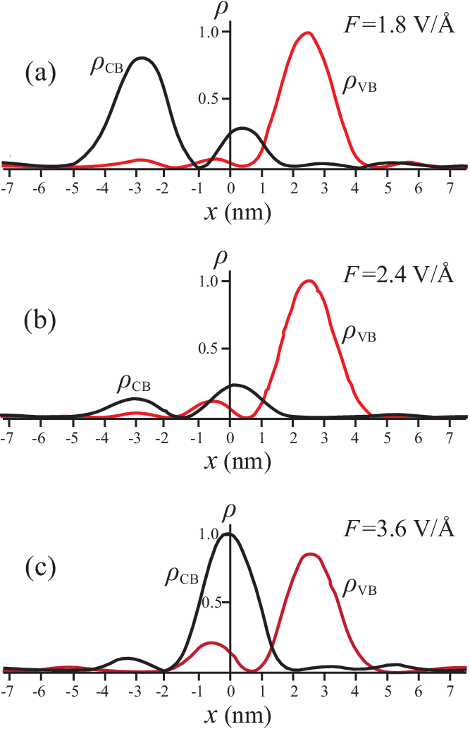
To illustrate the interband mixing introduced by an electric field, we show in Fig. 5 the conduction and valence band probability densities for the WS wave functions, i.e., and . The results are shown for one of the WS energy levels for a given electric field. The electric fields V/Å and V/Å are near and anticrossing points, respectively. In these cases, the interband mixing is strong, and the electron densities in the conduction and valence bands are comparable [see Fig. 5(a), (c)]. The spatial separation between the maxima of and is . Thus for V/Å, i.e., , the distance between the maxima of and is Å, while for V/Å, i.e., , the distance is Å.
For electric field V/Å, which is between and anticrossing points, the interband mixing is weak. In this case only one component (in our case only the valence band component, ) is strong [see Fig. 5(b)].
In both cases, i.e., at the anticrossing points and away from them, the wave functions are localized in the space. The localization length depends on the electric field. The points, at which the WS wave functions are localized, depend on the energy of the WS states. In Fig. 6 the total electron density, defined as , is shown for different WS states at electric field V/Å, which correspond to anticrossing point. With changing the energy of the WS state, the electron density distribution is shifted as a whole along the axis.

III.3 Wannier-Stark states of two-band model: numerical results
In the previous Section, analytical results for the WS spectra of the tight-binding model were obtained in the case of the -function dipole matrix elements. Such strong dependence of the dipole matrix element on the wave vector occurs near the Dirac points. Away from the Dirac points, the dipole matrix element as a function of the wave vector has a broad peak. In such a case, the WS energy spectra can be obtained numerically.
It is convenient to solve the system of the eigenvalue equations, (8)-(9), by expanding functions and in terms of the WS wave function of individual bands, Eqs. (14) and (20), calculated without interband coupling. Thus
| (49) | |||
| (50) |
where index labels the WS states [see Eqs. (15) and (18)], and are the corresponding expansion coefficients. Substituting expressions (49) and (50) into Eqs. (8)-(9), we obtain the system of eigenvalue equations on expansion coefficients and ,
| (51) | |||
| (52) |
where are dipole matrix elements, calculated between the WS wave functions of individual bands,
| (53) |

In Fig. 7, the energy spectra of a finite size system of graphene, calculated numerically from the system of equations (49)-(50), are shown for different value of the component of the wave vector, . At [see Fig. 7(a)], the system is far away from the Dirac points. In this case, the dipole matrix element as a function of has a broad peak [see Fig. 3]. For [see Fig. 7(b)], the system is close to the Dirac point with the dipole matrix element having a sharp narrow peak. In this case, the values of the anticrossing gaps and the positions of the anticrossing points are close to the analytical expressions (41) and (42), obtained in the model with -function profile for the dipole matrix element.
The data, shown in Fig. 7, illustrate strong dependence of the spectra on the value of , i.e. on the shape of the function . With increasing , i.e. when the peak in becomes sharp, the anticrossing points move to smaller values of electric field and the anticrossing gaps become smaller.
In Fig. 8, the anticrossing gaps and the positions of the anticrossing points are shown as a function of for and anticrossing points. A general trend is that with increasing , both the anticrossing gaps, , and the electric fields, , at which the anticrossing points are observed, are decreasing. The arrows in Fig. 7 show the analytical values of the anticrossing gaps and the positions of the anticrossing points, obtained from Eqs. (41) and (42). These numbers are close to the corresponding numerical values at , i.e. near the Dirac point [see Fig. 7].

III.4 Wannier-Stark states of two-band model: two Dirac points
By changing the direction of electric field, one can realize a situation when along a line of coupled states there are two Dirac points. For graphene, this happens for a line shown in Fig. 9(a), i.e. when the angle between the direction of the electric field and axis is . Then for the line, shown in Fig. 9, we introduce one dimensional wave vector, , along the direction of electric field and write the dipole matrix element in terms of two -functions, localized at the Dirac points,
| (54) |
where and are the coordinates of the Dirac points along the line of coupled states. The wave vector changes from 0 to , where determines the period of the system along the direction of electric field.
We follow the same steps as in the case of one Dirac point (see Sec. III.2). Namely, we introduce three regions, , , and . In each region, the conduction and valence bands become decoupled and the wave functions have the form of Eqs. (24)-(25). At the boundary between the regions, i.e. at points and , the boundary conditions have the form of Eqs. (28)-(29). Combining all these equations and taking into account the periodic boundary conditions at poins and , we obtain the following energy spectra of the coupled WS states
| (55) | |||||
Here is defined in terms of the linear integral over the line of coupled states (see Fig. 9),
| (56) |
The coefficient in Eq. (55) is defined by the following relation
| (57) |
In dimensionless variables, and , Eq. (55) becomes
| (58) | |||||
In Fig. 9(b) the dimensionless WS energy spectrum (58) is shown for parameters and , which correspond to graphene. Specific feature of this spectrum is a nonmonotonic dependence of the anticrossing gaps on the value of the dimensionless band offset, . These gaps have both large and very small values. The positions of the anticrossing points are also irregular. The corresponding energy spectrum in the original units is shown in Fig. 9(c) as a function of electric field . The anticrossing gaps have nonmonotonic dependence on . For example, the anticrossing gap at is larger than the gap at . This behavior is different from the behavior of the anticrossing gaps of the WS spectrum for systems where the dipole matrix elements are almost constant [16] or have a single peak as a function of the wave vector (see Sec. III.2).

IV Conclusion
Within a single (either conduction or valence) band model, the energy spectrum of an electron in graphene in a constant external field has a WS ladder structure with energy levels separated by the Bloch frequency, which is proportional to both the electric field and the lattice period of graphene crystal structure in the direction of electric field. In a two-band model, which is introduced above within the tight-binding nearest-neighbor approximation, a constant electric field results in mixing of the conduction and valence bands. As a result of such mixing, the energy spectrum of graphene as a function of electric field shows anticrossing points with the corresponding anticrossing gaps. These gaps also indicate that a constant electric field opens a gap in the electron energy spectrum of graphene. This is understandable because it reduces symmetry of the system by lifting the equivalence (degeneracy) of the two constituent triangular sublattices. The magnitudes of the gaps depend on the electric field.
The strength of the band mixing in an external electric field is determined by the magnitude of the interband dipole matrix element. The net (integral) interband dipole matrix element has a value of universally determined by the Pancharatnam-Berry phase.
In graphene, this interband dipole matrix element has unique dependence on the electron wave vector. Namely, at the Dirac points, it has sharp peaks, i.e., in the reciprocal space, the interband coupling is strong near the Dirac points only. In this case, approximating such a strong dependence of the dipole matrix element on the wave vector by the -function, one can find an analytical expression for the WS energy spectrum. Such analytical solution predicts both the positions of the anticrossing points and the corresponding anticrossing gaps. As a function of inverse electric field the anticrossing points are equidistant. In the dimensionless units (relative to the Bloch frequency), the anticrossing gaps have the same value at all anticrossing points. Thus, in the original energy units, the anticrossing gaps are proportional to the electric field at the corresponding anticrossing points and, for graphene, are (eV), where is an integer. Physically, such an anticrossing gap (divided by ) is the rate of the Zener tunneling through unit cells that transfers an electron in a localized WS state from the valence to the conduction band. The largest anticrossing gap eV corresponds to the anticrossing point at the electric field V/Å. The weak dependence, of the anticrossing gaps on parameter is a unique property of graphene and is due to highly nonuniform, singular profile of the dipole matrix element.
Such high fields, , can be generated only by laser pulses in the visible/near-infrared [17, 18] or terahertz [11] spectral regions. Graphene in a time-dependent electric field (see, for example, Ref. [32]), when the electron dynamics is described in terms of the passage of the anticrossing points, the anticrossing gaps determine the characteristic time, fs, which characterizes adiabaticity of the dynamics. Namely, if time of passage of an anticrossing point, which is also the characteristic time of variation of electric field, is much larger than , , then the electron dynamics is adiabatic. For example, if fs, then the passages of anticrossing points and 2, which have the characteristic times fs and 0.51 fs, are adiabatic, while the passages of the points is non-adiabatic or even diabatic. It is evident that no matter what is frequency range, from visible to terahertz, there always will be several anticrossings with near-resonant frequencies violating adiabaticity. Thus the rapid adiabatic passage [32] is not possible in graphene; also Rabi oscillations will be dephased.
Appendix
We express the general solution of the Schrödinger equation (1) - (2) in the form (7), i.e., in the basis of eigenfunctions of field-free Hamiltonian . Substituting expression (7) for the wave function into the Schrödinger equation (1) - (2), we obtain
| (59) |
We multiply both sides of Eq. (59) by and then integrate it by . Taking into account that are eigenfunctions of Hamiltonian , we obtain
| (60) |
Substituting explicit expression (6) for , we rewrite the second term in the right hand side of Eq. (60) as follows
| (61) |
where in the last line, in the sum (integral) over , we use integration by parts. The final expression contains an additional term , which is not included in the system of equations (8)-(9) since this term can be eliminated by substitution and does not affect the energy spectrum of the system.
The third term in the right hand side of Eq. (60) can be rewritten as
| (62) |
where the term proportional to is zero due to orthogonality of the conduction and valence band free-field functions:
| (63) |
Combining Eqs. (60)-(62), we obtain Eq. (8). Similarly, multiplying Eq. (59) by and integrating it by , we can derive Eq. (9).
Acknowledgment
This work was supported by MURI grant N00014-13-1-0649 from the US Office of Naval Research, grant No. DE-FG02-11ER46789 from the Materials Sciences and Engineering Division, Office of the Basic Energy Sciences, Office of Science, U.S. Department of Energy, Grant No. DE-FG02-01ER15213 from the Chemical Sciences, Biosciences and Geosciences Division, Office of the Basic Energy Sciences, Office of Science, U.S. Department of Energy, and NSF grant No. ECCS-1308473. MIS gratefully acknowledges also support by the Max Planck Society and the Deutsche Forschungsgemeinschaft Cluster of Excellence: Munich Center for Advanced Photonics (http://www.munich-photonics.de) during his Sabbaticals at Munich.
References
- [1] F. Bloch, Z. Phys. A 52, 555 (1929).
- [2] C. Zener, Proc. Royal Soc. A 145, 523 (1934).
- [3] G. H. Wannier, Elements of Solid State Theory (Cambridge University Press, Cambridge, England, 1959).
- [4] G. H. Wannier, Phys. Rev. 117, 432 (1960).
- [5] J. Bleuse, G. Bastard, and P. Voisin, Phys. Rev. Lett. 60, 220 (1988).
- [6] E. E. Mendez, F. Agullo-Rueda, and J. M. Hong, Phys. Rev. Lett. 60, 2426 (1988).
- [7] J. Feldmann, K. Leo, J. Shah, D. A. B. Miller, J. E. Cunningham, T. Meier, G. von Plessen, A. Schulze, P. Thomas, and S. Schmitt-Rink, Phys. Rev. B 46, 7252 (1992).
- [8] E. E. Mendez and G. Bastard, Phys. Today 46, 34 (1993).
- [9] T. Dekorsy, P. Leisching, C. Waschke, K. Kohler, K. Leo, H. G. Roskos, and H. Kurz, Semicond. Sci. Tech. 9, 1959 (1994).
- [10] S. Ghimire, A. D. DiChiara, E. Sistrunk, P. Agostini, L. F. DiMauro, and D. A. Reis, Nature Phys. 7, 138 (2011).
- [11] O. Schubert, M. Hohenleutner, F. Langer, B. Urbanek, C. Lange, U. Huttner, D. Golde, T. Meier, M. Kira, S. W. Koch, et al., Nat. Phot. 8, 119 (2014).
- [12] A. D. DiCarlo, P. Vogl, and W. Pötz, Phys. Rev. B 50, 8358 (1994).
- [13] B. Rosam, K. Leo, M. Gluck, F. Keck, H. J. Korsch, F. Zimmer, and K. Kohler, Phys. Rev. B 68, 125301 (2003).
- [14] M. Gluck, A. R. Kolovsky, and H. J. Korsch, Journal of Optics B: Quantum and Semiclassical Optics 2, 694 (2000).
- [15] M. Gluck, A. R. Kolovsky, and H. J. Korsch, Phys. Rep. 366, 103 (2002).
- [16] V. Apalkov and M. I. Stockman, Phys. Rev. B 86, 165118 (2012).
- [17] A. Schiffrin, T. Paasch-Colberg, N. Karpowicz, V. Apalkov, D. Gerster, S. Muhlbrandt, M. Korbman, J. Reichert, M. Schultze, S. Holzner, et al., Nature 493, 70 (2012).
- [18] M. Schultze, E. M. Bothschafter, A. Sommer, S. Holzner, W. Schweinberger, M. Fiess, M. Hofstetter, R. Kienberger, V. Apalkov, V. S. Yakovlev, et al., Nature 493, 75 (2012).
- [19] A. K. Geim and K. S. Novoselov, Nat. Mater. 6, 183 (2007).
- [20] A. H. C. Neto, F. Guinea, N. M. R. Peres, K. S. Novoselov, and A. K. Geim, Rev. Mod. Phys. 81, 109 (2009).
- [21] D. S. L. Abergel, V. Apalkov, J. Berashevich, K. Ziegler, and T. Chakraborty, Adv. Phys. 59, 261 (2010).
- [22] A. R. Kolovsky and E. N. Bulgakov, Phys Rev A 87, 033602 (2013).
- [23] P. R. Wallace, Phys. Rev. 71, 622 (1947).
- [24] J. C. Slonczewski and P. R. Weiss, Phys. Rev. 109, 272 (1958).
- [25] R. Saito, G. Dresselhaus, and M. Dresselhaus, Physical Properties of Carbon Nanotubes (Imperial College Press, London, 1998).
- [26] S. Reich, C. Thomsen, and J. Maultzsch, Carbon Nanotubes (Wiley-VCH, Weinheim, 2004).
- [27] S. Pancharatnam, Proc. Indian Acad. Sci. A 44, 247 (1956).
- [28] M. V. Berry, Proc. Royal Soc. 392, 45 (1984).
- [29] J. Zak, Phys. Rev. Lett. 62, 2747 (1989).
- [30] R. Resta, Rev. Mod. Phys. 66, 899 (1994).
- [31] D. Xiao, M.-C. Chang, and Q. Niu, Rev. Mod. Phys. 82, 1959 (2010).
- [32] H. K. Avetissian, G. F. Mkrtchian, K. G. Batrakov, S. A. Maksimenko, and A. Hoffmann, Phys. Rev. B 88, 245411 (2013).