david.bowler@ucl.ac.uk
Hydrogen adsorption and diffusion around Si(001)/Si(110) corners in nanostructures
Abstract
While the diffusion of hydrogen on silicon surfaces has been relatively well characterised both experimentally and theoretically, the diffusion around corners between surfaces, as will be found on nanowires and nanostructures, has not been studied. Motivated by nanostructure fabrication by Patterned Atomic Layer Epitaxy (PALE), we present a density functional theory (DFT) study of the diffusion of hydrogen around the edge formed by the orthogonal (001) and (110) surfaces in silicon. We find that the barrier from (001) to (110) is approximately 0.3 eV lower than from (110) to (001), and that it is comparable to diffusion between rows on the clean surface, with no significant effect on the hydrogen patterns at growth temperatures used.
1 INTRODUCTION
Historically, bulk silicon chip fabrication has been a planar process based on repetitive optical lithography. The progressive reduction in device surface area has impaired switching characteristics, leading to the introduction of three-dimensional structures (e.g. finFETs) that can be realized in planar processes. This trend has prompted interest in other ways of engineering three-dimensional silicon growth [1] such as Patterned Atomic Layer Epitaxy (PALE) [2, 3]. PALE utilizes chemical vapour deposition (CVD) to create silicon features without the conventional lithography and masking steps. In this paper we use density functional theory (DFT) to consider how hydrogen diffusion around feature edges affects the growth process.
In PALE a hydrogen-passivated Si(001) substrate can be patterned by selective removal of the hydrogen atoms using an STM probe in UHV conditions [2, 3, 4]: the exposed dangling bonds provide adsorption sites for Si fragments deposited from disilane gas admitted into the STM chamber, a form of UHV-CVD. In principle, an atomically-precise three-dimensional structure of any height could be grown by successive depassivation and deposition steps. In practice the quality of the grown layers depends critically on the effectiveness of the depassivation process, which tends to fall as growth proceeds. This leads to surface roughening and the eventual breakdown of epitaxial growth [4].
CVD reactions are complex with multiple pathways through the adsorption, deposition and desorption phases [5, 6]. On the clean Si(001) surface, the disilane molecule dissociates into SiH2 groups with accompanying atomic hydrogen. When these groups occur on adjacent surface sites they form monohydride dimers [5, 7] which grow into strings and islands upon further disilane deposition. The hydrogen is adsorbed directly on the substrate and slowly desorbs into molecular gas. The ad-dimers and atomic hydrogen compete for unreacted substrate sites, whose availability determines the overall reaction rate. Conventional low pressure CVD is conducted at relatively high (around 1000 K) temperatures and the growth rate is determined by precursor throughput. With PALE the ambient temperature cannot exceed 550 K otherwise the passivating H-layer is destabilized. At this temperature, desorption is incomplete and atomic hydrogen remains bound to the substrate, preventing completion of the first monolayer. Now the surface is saturated with a variety of Si–H configurations and further depassivation is necessary. Completion of the first layer typically occurs after 3 or 4 depassivation and deposition cycles [4].
Surface coverage is also affected by hydrogen diffusion at the prevailing temperature. H adatoms have been shown to diffuse along trenches in the the (011) surface with energy barrier of the order 1 eV [8]. Other theoretical calculations on the (001) surface predict somewhat larger barriers, i.e. 1.6 eV [9] to 1.7 eV [10, 11], in agreement with experiment [9] . In this study, we use DFT to study H adatoms on the top and side walls of a notional PALE nanostructure, a simple pillar with a horizontal (001) growth surface. The sidewalls are assumed to have the (110) orientation, a surface of technological interest due to its high carrier mobility. We investigate whether diffusion pathways around the corners would inhibit growth, increasing the number of depassivation/deposition cycles required per monolayer thus rendering PALE impractical. We construct a supercell containing both the (001) and (110) faces and and seek possible diffusion paths around the corners between these faces. Finally we calculate the energy barrier between the two faces and discuss the likely effect on the PALE growth process.
2 METHODS
2.1 Computational details
All calculations used density functional theory [12], as implemented in the Vienna Ab-initio Simulation Package [13] (VASP version 4.6.34) with the Perdew-Burke-Enzerhof (PBE) generalised gradient approximation (GGA) exchange-correlation functional [14]. The VASP projector-augmented-wave [15, 16] (PAW) potentials for silicon and hydrogen were used. The PAW-PBE potential file (POTCAR) for the silicon atom was dated 5th January 2001 and that for hydrogen 15th June 2001. We used a 200 eV energy cutoff. The Brillouin zone was sampled with a Monkhorst-Pack mesh [17]. Gaussian smearing was applied to fractional occupancies with a width of 0.1 eV. The convergence criterion for forces on atoms was 0.01 eV/Å and for total energy 10-4 eV. These parameters yield relative energies and energy barriers reliable to within 0.01 eV. We used the FIRE algorithm [18] to optimize the structures. Structural relaxations for hydrogen adsorption and diffusion pathways used the quasi-Newton method implemented in VASP.
Transition state search was performed using the climbing image nudged elastic band method as implemented in the VASP Transition State Tools [19, 20] (VTST) code. The climbing image variation of NEB converges rigorously onto the highest saddle point using just a single intermediate point and yields accurate barrier energy values [21].
2.2 The supercell
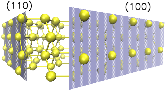
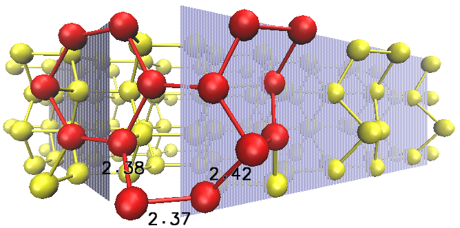
We used a chevron-shaped supercell with a 28 Å 8 Å cross section with the vertical perpendicular in the (112) direction (Figure 1). This orientation exposes approximately equal (001) and (110) surface areas at the apex. A vacuum spacing of 14 Å was interposed and terminating H atoms added between periodic images. We used the experimental bulk Si lattice parameter (5.431 Å), which is in good agreement with the calculated value for this DFT setup. The supercell depth was determined empirically by adding base layers until the change in energy decrement E was less than 0.01 eV. The Monkhorst-Pack sampling grid was established in a similar way and set to 6 2 1. The final structure had a depth of 50 Å and contained 350 Si atoms. The reconstruction of the of the apex region is shown in Figure 2 (lower). We also tested a smaller supercell with a 18 Å 8 Å cross section and 160 atoms but found that the reconstruction at the apex showed evidence of strain from the base layers which disappeared when the structure was enlarged.
All coordinate files are available freely on figshare [22].
2.3 Finding H adsorption sites and diffusion pathways
The H adsorption sites are likely to be 3-coordinate on the (110) surface or dimers on the (001) surface. In both cases a single dangling bond is exposed and its replacement by a covalent Si–H bond causes a reduction in the total energy. We placed a H atom 1.5 Å above each potential adsorption site on the reconstructed surface (in the direction of the dangling bond) and re-optimized the structure. Total structure energy was typically reduced by approximately 4 eV when compared to the clean structure. Binding energies of the adsorbed hydrogen atom were calculated with respect to the energy of a gaseous molecule:
| (1) |
where , and represent the total energy of the optimised structure with the adsorbed H atom, the optimised energy of the clean Si reconstruction and the total energy of gas-phase hydrogen molecule, respectively. A negative binding energy indicates an energy gain on adsoprtion; a positive binding energy indicates an energy loss. A diffusion pathway will be formed between two adjacent adsorption sites provided that the energy required to surmount any intervening energy barriers is comparable with the thermal energy acquired by the mobile atom. We select the lowest energy sites close to the step edge and use the NEB climbing-image optimizer to find the diffusion barriers. We then use the Arrhenius equation to estimate the diffusion rate across the edge.
3 RESULTS AND DISCUSSION
3.1 Reconstruction and characterization
As the (001) surface normal swings through a right-angle to the (110) direction it passes through a number of intermediate surface planes e.g. [114], [113], [111], [331] [23]. Each of these surfaces has its own reconstruction strategy but all contain the prototypical 3-coordinate surface atom found on the bulk-truncated (111) surface. Consequently we can expect the reconstruction to of the apex region to include the hexagonal pattern seen on the (111) unreconstructed surface. This can be seen in Figure 2 (upper), while the relaxed structure can be seen in Figure 2 (lower), which also shows the extended bond lengths expected in the presence of delocalized electrons. Away from the apex, the figure shows characteristic dimerization and buckling on the (001) surface and out-of-plane buckling of the zig-zag rows of the (110) surface. Distortion in the bulk structure is greatest in the region beneath the apex and extends to a depth of 20 Å. These observations suggest that the reconstruction is plausible, offering a sensible basis for the calculation of a model potential energy surface. An exhaustive characterization of the step edge reconstruction would require examination of larger structures in multiple orientations and is beyond the scope of this work.
3.2 The potential energy surface
We investigated 16 possible adsorption sites on the reconstructed surfaces. Six of these gave total energies falling within a 0.3 eV range while the remainder was at least 1 eV higher and not considered further further (an increment of 1 eV reduces the adsorption probability by a factor of ). These values are shown in Table 1 and the sites depicted in Figure 3.
| Site | Relative energy | Binding energy |
|---|---|---|
| 1 | 0.29 | -1.65 |
| 2 | 0.06 | -1.88 |
| 3 | 0.00 | -1.95 |
| 4 | 0.02 | -1.92 |
| 5 | 0.29 | -1.65 |
| 6 | 0.13 | -1.81 |
Sites 3, 4 and 5 are situated on the chevron apex so we considered a diffusion path consisting of the two hops 3–4 and 4–5. Each is analogous to the kinetics of a chemical reaction with a single transition state corresponding to the highest saddle point in the potential energy landscape lying between the end points. The climbing image variation of NEB returns the energy at the highest saddle point and so a single-image NEB calculation per hop suffices in this case. Additional images can provide further points on the reaction path corresponding to the route taken by diffusing atoms, although the computational cost is considerable. Since we are interested only in relative barrier heights, we elect to perform single-image calculations.
| End-point | Energy | ||
|---|---|---|---|
| 3 | -1947.01 | ||
| barrier | -1945.44 | 1.57 | 1.55 |
| 4 | -1946.98 | ||
| barrier | -1945.00 | 1.99 | 1.72 |
| 5 | -1946.71 |
These results of the NEB calculations values are shown in Table 2 and represented graphically in Figure 4. Figure 3 (lower) gives a rough indication of the actual diffusion path. The effective barrier for the path is the greater of the hop barriers and is asymmetrical, due to the differing starting energies. Diffusion from (001) to (110) has a barrier of 1.72 eV, while the reverse process has a barrier of 1.99 eV. These can be compared with published values of 1.66 eV 0.15 eV [10] and 1.75 0.02 eV [9] for intrarow H diffusion on the (001) surface and 1.17 eV (intra row) and 1.49 eV (inter row) on the Si(110) surface[8]. The diffusion from the top of the pillar (the (001) surface) to the side of the pillar (the (110) surface) has a comparable barrier to diffusion on the Si(001) surface, while diffusion in the opposite direction has a significantly larger barrier.
4 Discussion and Conclusions
We have studied the stability of hydrogen adatoms at positions near the intersection of the Si(001) and (110) surfaces, as might be found on a nanopillar grown on Si(001) by patterned ALE. We have identified a diffusion pathway around the corner and calculated the barrier energies on it. We find that that the hydrogen is more stable on the (110) face than the (001) face.
In the PALE context we are concerned with whether hydrogen will leave the top of the nanopillar for the sidewall or vice versa. The process involves a disilane gas source and leaves hydrogen on the sidewalls. Hydrogen migration onto the growth surface would interfere with subsequent STM lithography and possibly compromise the entire process. From the barriers we can see that, at least for this configuration, diffusion off the top of a nanopillar will only be activated once diffusion on the substrate is activated and diffusion back onto the top will occur only at higher temperatures. The difference in barrier energy ( 0.3 eV) is significant in DFT terms and equivalent to a temperature increase of 100 K.
The actual diffusion rate () can be estimated from the energy barrier by the Arrhenius equation
| (2) |
where is the attempt frequency, the energy barrier, the Boltzmann constant and the ambient temperture. is generally found to lie in the range and since the rate expression is dominated the negative exponential energy term we can take to get an upper bound on the rate. If the PALE process temperature of 550 K is assumed and adsorption sites are assumed to be occupied with a probability of one, then we could estimate a rate of or approximately one diffusion event every 10 minutes off the nanopillar. The reverse process would be three hundred times less frequent at 550K.
We can extrapolate from this single event to an entire nanopillar, under the conditions used in PALE. A pillar with a side of 5 nm would have 100 edge sites available, generating a diffusion event off the pillar every 5 or 6 seconds, assuming that there was a empty site to reach. The reverse process produces a diffusion event every half hour. These results indicate that there would be net hydrogen migration off the pillar, which is a desirable outcome in PALE terms. There is little reason to be concerned about higher temperatures, as the process temperature of 550K is chosen to avoid desorption of the hydrogen resist (it begins to show mobility at temperatures exceeding 600K).
Although sidewall hydrogen diffusion may not be a critical issue in a PALE manufacturing process other obstacles remain. Chief amongst these is the the formation of anti-phase boundaries (APBs) in the growth surface due to the collision of islands with different registry. These APBs can trap hydrogen beneath the surface, leading to a reduction in the depassivation yield from subsequent STM lithography. The reduction in yield can be mitigated by adjusting the STM parameters prior to each depassivation step, but the remanent hydrogen causes cumulative surface damage which halts epitaxial growth after 2 or 3 monolayers. The remediation of APBs and improvement of the quality of the silicon is the subject of ongoing research.
5 ACKNOWLEDGEMENTS
We acknowledge useful discussions with James Owen and John Randall of ZyvexLabs.
References
- [1] Martin C 2014 Nat Nano 9 89
- [2] Lyding J W, Abeln G C, Shen T C, Wang C, and Tucker J R 1994 J. Vac. Sci. Technol. B 12 3735
- [3] Shen T C, Wang C, Abeln G C, Tucker J R, Lyding J W, Avouris P, and Walkup R E 1995 Science 268 1590
- [4] Owen J H, Ballard J, Randall J N, Alexander J, and Von Ehr J R 2011 J. Vac. Sci. Technol. B 29 06F201
- [5] Owen J H G, Miki K, Bowler D R, Goringe C M, Goldfarb I, and Briggs G A D 1997 Surf. Sci. 394 79
- [6] Owen J H G, Miki K, Bowler D R, Goringe C M, Goldfarb I, and Briggs G A D 1997 Surf. Sci. 394 91
- [7] Bowler D R 2003 Phys. Rev. B 67 115341
- [8] Brázdová V and Bowler D R 2011 Phys. Chem. Chem. Phys. 13 11367
- [9] Owen J H G, Bowler D R, Goringe C M, Miki K, and Briggs G A D 1996 Phys. Rev. B 54 14153
- [10] Bowler D R, Fearn M, Goringe C M, Horsfield A P, and Pettifor D G 1998 J. Phys.: Condens. Matter 10 3719
- [11] Dürr M and Höfer U 2013 Prog. Surf. Sci. 88 61
- [12] Kohn W 1999 Rev. Mod. Phys. 71 1253
- [13] Kresse G and Furthmüller J 1996 Phys. Rev. B 54 169
- [14] Perdew J P, Burke K, and Ernzerhof M 1996 Phys. Rev. Lett. 77 3865
- [15] Blöchl P E 1994 Phys. Rev. B 50 17953
- [16] Kresse G and Joubert D 1999 Phys. Rev. B 59 1758
- [17] Monkhorst H J and Pack J D 1976 Phys. Rev. B 13 5188
- [18] Bitzek E, Koskinen P, Gähler F, Moseler M, and Gumbsch P 2006 Phys. Rev. Lett. 97 170201
- [19] Henkelman G, Uberuaga B P, and Jonsson H 2000 J. Chem. Phys. 113 9901
- [20] Sheppard D, Terrell R, and Henkelman G 2008 J. Chem. Phys. 128
- [21] Klimes J, Bowler D R, and Michaelides A 2010 J. Phys.: Condens. Matter 22 074203
- [22] Smith R L and Bowler D R DOI:10.6084/m9.figshare.940993
- [23] Battaglia C, Gael-Nagy K, Monney C, Didiot C, Schwier E F, Garnier M G, Onida G, and Aebi P 2009 J. Phys.: Condens. Matter 21 013001