Ground state of graphene heterostructures in the presence of random charged impurities.
Abstract
We study the effect of long-range disorder created by charge impurities on the carrier density distribution of graphene-based heterostructures. We consider heterostructures formed by two graphenic sheets (either single layer graphene, SLG, or bilayer graphene, BLG) separated by a dielectric film. We present results for symmetric heterostructures, SLG-SLG and BLG-BLG, and hybrid ones, BLG-SLG. As for isolated layers, we find that the presence of charged impurities induces strong carrier density inhomogeneities, especially at low dopings where the density landscape breaks up in electron-hole puddles. We provide quantitative results for the strength of the carrier density inhomogeneities and for the screened disorder potential for a large range of experimentally relevant conditions. For heterostructures in which BLG is present we also present results for the band-gap induced by the perpendicular electric field generated self-consistently by the disorder potential and by the distribution of charges in the heterostructure. For SLG-SLG heterostructures we discuss the relevance of our results for the understanding of the recently observed metal-insulator transition in each of the graphene layers forming the heterostructure. Moreover, we calculate the correlation between the density profiles in the two graphenic layers and show that for standard experimental conditions the two profiles are well correlated.
I Introduction
The ability to realize single layer graphene (SLG) [1], bilayer graphene (BLG) [2], and other two-dimensional (2D) crystals [3], combined with recent advances in fabrication techniques [4, 5] in recent years has allowed the realization of novel 2D heterostructures [6, 7, 8, 9, 10, 11, 12, 13, 14, 15, 16, 17]. In these structures, two or more 2D crystals are stacked in a designed sequence. Layers of hexagonal boron nitride (hBN) [18, 19, 20] have been used to electrically separate the graphenic layers (SLG or BLG) in multilayered 2D heterostructures. In particular, hBN allows the realization of graphene-based heterostructures in which the graphenic layers are very close and yet electrically separated [21, 22], a situation that is ideal to study the effects of interlayer interactions. It has been proposed that in these type of systems the interlayer interactions can drive the system into spontaneously broken symmetry ground states [23, 24, 25, 26, 27, 28]. So far, experiments have not observed clear signatures of the establishment of these collective ground states. However, recent measurements of the drag resistivity in graphene double layers [21] have shown that the drag resistivity has a very large and anomalous peak when the doping in both graphene sheets is set to zero. This phenomenon indicates that a strong correlation is present between the carriers in the two layers.
In most of the samples random charge impurities are present in the graphene environment, either in the substrate or trapped between the graphenic layer and the substrate. It has been shown theoretically [29] and experimentally [30, 31, 32, 33] that the long-range disorder due to charge impurities induces strong, long-range, carrier density inhomogeneities in isolated SLG and BLG. The presence of random carrier density inhomogeneities has been predicted theoretically to strongly suppress the critical temperature () for the formation of an interlayer phase coherent state [34, 35, 36] in graphene heterostructures. This is in contrast to the short-range disorder that is not expected to suppress significantly [37, 28, 38]. In addition, the presence of charge inhomogeneities, correlated in the two layers, is a necessary ingredient of the energy-transfer mechanism that has been proposed [39, 40] to explain the strong peak of the drag-resistivity at the double-neutrality point. Disorder-induced carrier density inhomogeneities are also expected to strongly affect the transport properties of graphene-based heterostructures [41, 42, 43, 44, 45, 46]. For these reasons, the accurate characterization of the carrier density inhomogeneities induced by long-range disorder in graphene-based heterostructures is essential to understand the fundamental properties of these systems and to identify ways to increase their electronic mobility.
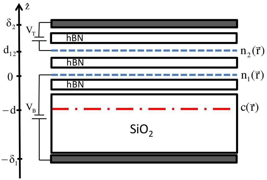
The characterization of the effects of disorder in graphene-based heterostructures is challenging for several reasons: (i) In most samples the disorder appears to be due predominantly to random charge impurities and to be quite strong and long-range, this fact makes the use of standard techniques, such as perturbation theory, not viable; (ii) Due to the linear dispersion in graphene, the screening of the long-range disorder due to the charge impurities is nonlinear; (iii) In graphene heterostructures the screening effects due to the different layers must be taken into account self-consistently; (iv) In bilayer graphene the presence of a perpendicular electric field opens a band-gap [47, 48]; (v) In heterostructures comprising BLG the component of the electric field perpendicular to BLG, and the BLG gap, must be obtained self-consistently taking into account the presence of the disorder and its screening by the metallic gates, and the other graphenic layer. In this work we present a systematic study of the effects of the long-range disorder due to random charge impurities on the ground state of graphene-based heterostructures taking into account all the effects mentioned above. As shown in Fig. 1 we consider heterostructures formed by two “graphenic” layers, either SLG or BLG, separated by a thin dielectric film. In the assumed configuration, using a top and a bottom gate, the doping of each graphenic layer can be set independently. We considered three classes of heterostructures: (i) double layer graphene (SLG-SLG) formed by two sheets of single layer graphene; (ii) double bilayer graphene (BLG-BLG) formed by two sheets of bilayer graphene; (iii) “hybrid structures” (BLG-SLG) formed by one sheet of BLG and one sheet of SLG. We find that the presence of charge impurities induces strong and long-range carrier density inhomogeneities in graphene-based heterostructures as in isolated SLG [29] and BLG [43]. However, for typical experimental situations we find that for the top graphenic layer the strength of the carrier density inhomogeneities is strongly suppressed due to the screening of the charge impurities by the bottom layer. We quantify this effect for most of the experimentally relevant conditions and find that for the top layer the amplitude of the density fluctuations can be reduced by an order of magnitude and that the effect is strongest in BLG-SLG heterostructures. We also show that the carrier density inhomogeneities in the different graphenic layers are well correlated. Finally, we show how the average band gap of BLG and its root mean square depend on the parameters, such as the impurity density, characterizing the heterostructure. Our results present a comprehensive characterization of the carrier density profile of graphene heterostructures in the presence of long-range disorder. By showing how the strength of the carrier density inhomogeneities depend on the experimental parameters, our results show how the quality of graphene-based heterostructures could be improved. In particular, the parameters that, within a certain range, can be easily tuned experimentally are: the doping of each of the graphenic sheets forming the heterostructure, the type of graphenic sheets used, the impurity density (via annealing or the use of different substrates), and the distance between the graphenic sheets. For each of these parameters we present quantitative results that show how the values can be tuned to reduce the disorder strength in each of the graphenic sheets, or both, forming the heterostructure. The results presented in the remainder of this work, for instance, quantify how an increase of the doping in one of the two sheets forming the heterostructure can substantially reduce the strength of the disorder-induced long-range inhomogeneities in the other sheet, and quantify how much a reduction of the impurity density would reduce the strength of the disorder potential in the heterostructure. In addition, we show how a change of the distance between the two sheets can be optimized to reduce the overall disorder strength in the heterostructure. Our results also show that, to reduce the strength of the disorder-induced long-range inhomogeneities in single layer graphene it is more efficient to have below it a sheet of bilayer graphene instead of SLG. The information on how to reduce, control, the disorder strength is essential for the study of fundamental effects in graphene heterostructures and for their use in technological applications.
In section II we present our theoretical approach; in section III we present the results and discuss their relevance for current experiments; in section IV we discuss the relevance of our results for the recently observed metal-insulator transition as a function of doping in double-layer graphene heterostructures. Finally in section V we present our conclusions.
II Theoretical approach
Figure 1 presents a sketch of the type of graphene heterostructure that we consider. One graphenic layer (SLG or BLG), layer 1 in our notation is placed on an insulating substrate, typically . A thin buffer layer of high quality dielectric, typically hBN, might be present between the and the graphenic layer. A second graphenic layer, layer 2, is placed above the first one. Layer 2 and layer 1 are electrically isolated via a thin insulating film. The doping level of the two graphenic layers can be tuned independently via a top and a bottom gate.
There is compelling evidence [45] that in systems of the type depicted in Fig. 1 the dominant sources of disorder are random charge impurities located close to the surface of . It is known that on the surface of there is a large density of charge impurities. Transport measurements on single layer graphene have consistently observed a linear scaling of the conductivity with the doping (), at low doping. The fact that the conductivity is suppressed at low dopings indicates that the effective strength of the disorder increases as the carrier density is decreased. Theoretical transport results in which charge impurities are the dominant source of scattering precisely predict at low dopings a linear suppression of the conductivity as is decreased [41, 49, 45]. The agreement between transport theories in which charge impurities are the main source of disorder and experimental transport measurements has also been confirmed by experiments in which the density of charge impurities was tuned [50]. In recent years there have been also several imaging experiments [30, 31, 32, 33] that, close to the charge neutrality point, have observed the presence of electron-hole puddles with dimensions and amplitudes that are consistent with the presence of charge impurity densities in the graphene environment [42, 41, 29] of the order of the ones extracted from the transport results mentioned above.
The distribution of the charge impurities can be modeled as an effective 2D distribution placed at a distance below the bottom graphenic layer (layer 1). The dash-dot line in Fig. 1 shows schematically the location of the effective 2D plane where the random impurities are located. It is likely that some charge impurities will also be trapped between each graphenic sheet and the adjacent thin dielectric films. However, experimental evidence, especially for setups in which hBN is used as dielectric material, strongly suggests that the density of such trapped impurities is at least an order of magnitude smaller that the density of the impurities close to the surface of the . For this reason we henceforth assume that the disorder potential is solely due to the charge impurities located close to the ’s surface. Without loss of generality, we can assume , where the angle brackets denote average over disorder realizations. Our formalism allows to easily take into account the presence of spatial correlation between the charge impurities [51, 52]. However, given the fact that in general the charge impurities are frozen and locked in a configuration that results from the fabrication process and that is not the thermodynamic equilibrium [53], we can assume that their position is uncorrelated so that , where is the charge impurity density.
At low energies the fermionic excitations of SLG are well described by a massless Dirac model with Hamiltonian [54, 45]:
| (1) |
where is the momentum operator, are the Pauli matrices in sublattice space, and ms-1 is the Fermi velocity. Recent experiments for graphene on hBN have shown evidence of the opening of a gap [9, 55]. Considering that the fact that there is a 1.8% lattice mismatch between graphene and hBN and the fact that in current experiments a twist angle between the graphene layer and the hBN is normally present, the mechanism by which the gaps open is still not completely understood [40, 56], but is thought to be arising from the explicit breaking of the ’AB’ sub-lattice symmetry in SLG due to the presence of the hBN substrate, and that it should not depend on the local electric field, but should depend on the twist angle between graphene and hBN in some complex manner. For our purposes this means that for SLG on hBN the band-gap, if present, can be assumed to be fixed and independent of the local doping and electric field created by the nearby gates. In the presence of a band gap the low-energy Hamiltonian for single layer graphene becomes:
| (2) |
At low energies the effective Hamiltonian describing the fermionic excitations in BLG is
| (3) |
where mme is the effective electron mass and is the band gap due a difference () in the electrochemical potential between the two layers of carbon atoms forming BLG.
In our case in Eq. (3) is due to the presence of a perpendicular electric field induced by the metal gates, the other graphenic layer, and the charge impurities surrounding the BLG sheet. If BLG is layer 1, i.e. it is the graphenic layer closest to the charge impurities, we have:
| (4) |
where is the distance between the two graphenic layers and nm is the distance between BLG and the bottom gate, Fig. 1. Notice that in general is not uniform, mostly due to the presence of the charge impurities. When BLG is layer 2 we have:
| (5) |
where nm is the distance between the first graphenic layer and the top metal gate, Fig. 1. Using these expressions for the perpendicular component of the electric field we can calculate . We have
| (6) |
where () if BLG is the bottom (top) graphenic layer, and nm is the BLG interlayer separation. Taking into account screening effects [57, 58, 59] the band gap of BLG due to a finite value of is given by the equation
| (7) |
where eV is the BLG interlayer tunneling amplitude [54].
To obtain the ground state carrier density distribution in the presence of charge impurities we use the Thomas Fermi Dirac theory (TFDT). The TFDT is a generalization of the Thomas-Fermi theory to include cases in which the electronic degrees of freedom behave as massless Dirac fermions, as in single layer graphene. In this case both the kinetic energy functional and the functional due to the exchange part of the Coulomb interaction are different from those valid for systems in which the electrons behave as massive fermions [29, 60]. In the TFDT the ground state of the system is obtained by minimizing the energy functional, , of the carrier density . The TFDT is similar in spirit to the density functional theory (DFT), the difference being that in the TFDT the kinetic energy is also approximated by a functional of the density, , whereas in the DFT it is treated via the full quantum-mechanical operator acting on the wave function . The TFDT returns accurate results as long as the length-scale of the carrier density inhomogeneities is larger than the Fermi wavelength . Prior results on SLG [29, 43] and BLG [61, 62] have shown that in graphene-based systems this inequality is satisfied for typical experimental conditions. The value of that enters in the inequality is the typical local value inside the “puddles” characterizing the inhomogenous carrier density landscape. At the charge neutrality point (CNP) , however, everywhere the local density is different from zero and therefore locally has a finite value. As a consequence, close to the CNP the average density cannot be taken as a measure of the typical carrier density inside the puddles and a better estimate is given by the density root mean square . Given that [29, 61] we have that the TFDT is valid at all densities as long as is not too small () [63]. This is confirmed by prior results on SLG [29, 43] and BLG [61, 62]. The two major advantages of the TFDT are: (i) Being a functional theory is not perturbative with respect to the strength of the density fluctuations and can therefore take into account nonlinear screening effects; (ii) It is computationally very efficient and this makes the TFDT able to return disorder-averaged results.
For the systems of interest, the TFDT energy functional will be a functional of the density profiles, , in the two graphenic layers. Neglecting exchange-correlation terms that have been shown to be small for most of the situation we are interested in [29, 61], the general form of the functional is:
| (8) |
where is the dielectric constant of the medium surrounding the graphenic layers, is the distance between the graphenic layers, is the bare disorder potential in layer , and is the chemical potential in layer . The second term in Eq. (8) is the Hartree part of the intralayer Coulomb interaction, the third term is the Hartree part of the interlayer Coulomb interaction, and the fourth is the one due to the disorder potential . Assuming that charge impurities close to the surface of are the dominant source of disorder we have
| (9) | ||||
| (10) |
The ground state is obtained by minimizing with respect to . This gives rise to two coupled equations. In general, for the cases we are interested in, the term is nonlinear. For the case of gapless SLG scales as the square-root of the density:
| (11) |
For the case of gapped SLG we have
| (12) |
For BLG, neglecting the presence of a nonzero band-gap (), depends linearly on . This fact allows us to obtain analytical results for the carrier density ground state of BLG-BLG heterostructures in the limit (see Sec. III). In the presence of a band gap the screening is strongly non-linear and this is reflected by the nonlinear dependence of with respect to the density. Taking into account the band-gap for BLG we have
| (13) |
The nonlinearities due to the term , and the need to self-consistently calculate for systems involving BLG imply that the solution of the TFDT equations can only be achieved numerically. We then solve these equations for many (500-1000) disorder realizations to obtain disorder-averaged results. The need to consider many disorder realization to accurately obtain the disorder-averaged values of the quantities characterizing the ground state makes the computational efficiency of the TFDT approach very valuable.
III Results

Figure 2 shows the profiles for a single disorder realization of the carrier density and of the screened disorder potential in each layer of a SLG-SLG heterostructure, at the neutrality point. We see that, as for the case of isolated SLG and BLG [30, 29, 31, 32, 33, 45], the carrier density profile breaks up in electron-hole puddles. We also notice that the amplitude of the density fluctuations and the strength of the screened disorder potential in the top layer is much smaller than in the bottom layer. This is due mostly to the screening of the charge impurities by the layer closer to the impurities. When the spectrum of SLG is gapped some regions of the samples will be insulating. This is shown by Fig. 3 which presents the density and screened disorder profiles for a single disorder realization in a SLG-SLG system in which the band-gap in both graphene layers is set equal to 20 meV. The white areas in Fig. 3 (a), (b) are insulating regions, i.e. regions in which the local chemical potential is within the band-gap and therefore contain no carriers.

The results shown in Figs. 2,3 show how the profiles of the density and disorder of the top layer and the bottom layer are different. The asymmetry between the profiles in the two layers will also be reflected in the transport properties as observed experimentally [64]. In particular, for our configuration in which the disorder is dominated by the charge impurities at the surface of the , we see that in the presence of a gap the insulating regions are substantially larger in the top layer than in the bottom layer. We discuss the effect of this asymmetry on the qualitative features of electronic transport in section IV.

Figure 4 shows the profiles for a single disorder realization of the carrier density, panels (a) and (b), and screened disorder potential, panels (c) and (d), in each layer of a hybrid BLG-SLG heterostructure at the charge neutrality point. In comparing Fig. 2 (a) and Fig. 4 (a), we notice that the carrier density inhomogeneities are much stronger for BLG than SLG (all the rest being the same). This is due to the difference in the low-energy band structure between SLG and BLG. Due to this difference, the price in kinetic energy to create a density fluctuation at low energies is much higher for SLG than BLG. Figure 4 (b) shows that the amplitude of the density fluctuations in the top layer (SLG) is much smaller in BLG-SLG than in the SLG-SLG. This is due to the fact that BLG, as the layer closer to the impurities, is much more efficient than SLG in screening the second layer from the disorder potential due to the charge impurities. This indicates that the mobility of SLG could be increased significantly when placed in a heterostructure in which the layer closest to the charge impurities is BLG. That this is the case is further confirmed by the disorder-averaged results that we present below.
Figure 4 (e) shows the profile for single disorder realization of the band-gap in BLG. We see that, due to the presence of the charge impurities, is very inhomogenous. In addition, we see that locally can be as large as 60 meV. One could then wonder why in correspondence with the regions where is large, the carrier density, Fig. 4 (a), locally does not go to zero. This is due to the fact that when the doping is set to zero in both layers the perpendicular electric field responsible for opening the band-gap is due to the charge impurities that we have assumed to be concentrated below the first layer. In these conditions, the regions in which is strong correspond to regions where the density of charge impurities is high and the induced carrier density is also high. In other words, for the conditions considered, regions where are also regions where the local value of the chemical potential is outside the gap as shown schematically in Fig. 4 (f). The scenario sketched in Fig. 4 (f) is not valid when a non-negligible density of charge impurities is also present above the top graphenic layers or between the two graphenic layers. Also, when the doping in one or both the two graphenic layers is not zero there will be a uniform contribution to and this can create regions where the chemical potential is within the gap.

Figure 5 shows the profiles for single disorder realization of carrier density, screened disorder potential, and gap, in both layers of a BLG-BLG heterostructure, at the neutrality point. As for the other heterostructures, we see that the screening by the first layer considerably reduces the amplitude of the density inhomogeneities in the second layer and of the screened disorder potential. In addition, the band gap in the second layer is quite smaller than that in the first layer as we see in Fig. 5 (e), (f).
A quantitative comparison between the theoretical and the experimental results is only possible by obtaining the disorder-averaged values of the quantities that are measured experimentally. In addition, the disorder-averaged characterization of the ground state carrier density distribution is an essential ingredient for the development of the transport theory in the presence of strong, disorder-induced, carrier density inhomogeneities [45].
For BLG-BLG heterostructures in the limit in which the band-gap is zero, we can obtain analytic expressions for the disorder-averaged quantities that characterize the density profile and the screened disorder potential from the TFDT equations. Below we will show that in some situations the results obtained by setting provide results for for and that well approximate the results obtained by calculating self-consistently. By minimizing the functional of BLG-BLG structures with with respect to the density profile in the first layer and the density profile in the second layer we find:
| (14) |
where is the Fourier transform of the carrier density profile in layer , if , and nm is the BLG screening length. Using the statistical properties of the impurity distribution we can calculate the root mean square of the carrier densities () and the screened disorder potential
We find:
| (15) | ||||
| (16) |
() where
| (17) |
and
| (18) |
Figure 6 shows the scaling of (and ) in the two layers as a function of and . As increases the amplitude of the carrier density inhomogeneities decreases rapidly. As increases, approaches the value found for a single BLG sheet [62] whereas decreases exponentially to zero.

As discussed in Sec. II when SLG is one of the constituents of the heterostructure, and/or when the BLG’s band-gap cannot be neglected, the TFDT equations can only be solved numerically due to the nonlinearity induced by the kinetic energy term. Below we present our results for the disorder-averaged quantities. Apart when explicitly indicated, all the results were obtained for nm samples with a spatial coarse-graining of 1 nm [65, 66]. For each case we used a number of disorder realizations, , large enough to guarantee that the results would not change if a larger number of disorder realizations were used. For the cases presented below we find that the results do not depend on when is larger than 500.

Figure 7 shows the root mean square of the carrier density and of the screened disorder potential in each layer of a SLG-SLG heterostructure. We see that the amplitude of the carrier density fluctuations in the first layer increases with and depends quite weakly on . Analogously, in the second layer increases with . This is due to the fact that as the doping increases more carriers are available to screen the disorder potential by creating high density electron (hole) puddles in correspondance of the valleys (peaks) of the bare disorder potential. However, we see that also depends significantly on . This is due to the fact that the first layer, being the closest to the charge impurities, is most responsible for the screening of the disorder potential and therefore significantly affects the amplitude of the density fluctuations in the second layer. Both and contribute to a decrease of the screened disorder potential in layer 1 and layer 2, as show by Fig. 7 (c) and (d). The results of Fig. 7 (b) and (d) confirm the conclusion that we derived from the single disorder realization results: due to the screening effect of the first layer the amplitude of the carrier density inhomogeneities and the strength of the screened disorder potential are weaker in layer 2 than in layer 1.

In presence of a band-gap in the graphene spectrum for SLG-SLG systems, the dependence of and on and is qualitatively similar to the gapless cases. In the presence of a gap it is interesting to also look at how the fraction of the area of graphene that is insulating, () for layer 1 (2), depends on the doping in the two layers, see Figs. 8 (e), (f). For relatively large impurity densities, such as considered for the results shown in Fig. 8 (e), (f), in layer 1 depend only weakly on the doping of layer 2, and vice versa. However, as we show in Fig. 15, and as we discuss in section IV, this is not the case at low impurity densities. In practice we have that when the screened disorder the effect of layer on of the other layer can be very significant.

For heterostructures in which BLG is present we need to account for the opening of a band-gap due to the presence of a perpendicular electric field. The calculation of the band-gap has to be done self-consistently due to the fact that the redistribution of the charges in the layer forming the heterostructure modifies the profile of the perpendicular component of the electric field, affecting the profile of the band-gap that itself affects the screening properties of the heterostructure. To test the importance of self-consistently calculating the profile of for a set of cases for BLG-SLG structures, we first performed the calculation setting equal to the value obtained from Eqs. (4), (6), (7) in the limit of homogenous density profiles in the two layers, with , and . We then redid the calculation by obtaining self-consistently. The comparison of the two sets of results is shown in Fig. 9 in which in the two layers and the average gap () are plotted as a function of for a fixed, non zero, value of : the curves with open symbols show the results obtained keeping fixed, whereas the curves with solid symbols show the results obtained by calculating self-consistently. We see that in general the value of obtained using the two approaches differ. For the case in which we have that the value of obtained self-consistently is reasonably approximated by the fixed value, , obtained assuming uniform carrier density profiles. However, for we find that the value of is significantly different from , Fig. 9 (d). The results of Fig. 9 show that the effect of the disorder cannot be captured by a simple average of a spatially homogenous theory and requires a self-consistent calculation of the parameters defining the local band-structure. All results that we present for heterostructures in which BLG is present were obtained calculating self-consistently.

For a fixed , , , Fig. 10 shows the dependence of the disorder averaged quantities characterizing the ground state of a BLG-SLG structure on the and . We see that amplitude of the density fluctuations and the strength of the screened disorder potential at low dopings depend almost exclusively on , the average carrier density in SLG, and only very weakly on , the average carrier density in BLG. This is due to the fact that at low dopings the band gap in BLG is quite small and so the density of states (DOS) of BLG is to good approximation constant, independent of . On the other hand, in SLG, due to the linear band dispersion, the DOS depends linearly on the doping . As a consequence at low dopings a change of has a negligible effect on the screening properties of the system whereas an increase (decrease) of increases (decreases) the screening due to the second layer, SLG. At high dopings the situation is complicated by the effect that a high average density on each layer has on the size of the gap in BLG, as shown in Fig. 10 (e). As a consequence the DOS in BLG is no longer almost independent of . This causes dependence of and on the value of . In particular, the asymmetry of and with respect to , for large values of , is due to the asymmetric dependence of on , Fig. 10 (e). Figure 10 (f) shows the root mean square of , . We see the is in general of the same order of , indicating the inhomogeneities of the band-gap in BLG are quite strong and cannot be treated perturbatively. In addition, we see that, qualitatively, depends on and in a similar way to . Another important feature of the results of Fig. 10 to notice is that when both and are large the size of the gap in BLG is comparable to the strength of the screened disorder potential. In these conditions we expect that the transport properties might be significantly affected by the presence of the band-gap and that BLG might behave as a bad-metal [62].
We now consider the BLG-BLG heterostructure. In this case both the top layer and the bottom layer can have a gapped band structure. Due to the fact that the band gap in both layers depends asymmetrically on and , Fig. 11 (e), (f), we find that and , in both layers, depend asymmetrically on the average carrier density of each layer, as shown in Fig. 11 (a)-(d). We also find that in both layers the r.m.s. of the band gap is of the same order as and that it scales with and qualitatively as . We notice that for the bottom layer the average band-gap is never larger than the r.m.s of screened disorder potential. On the other hand, for the top layer we have that at large and the average gap is larger than . As a consequence we expect that when and are large the bottom layer will behave as a bad metal and the top layer as a bad insulator [62].
By comparing the results of Fig. 7, 10, and 11, we see that the three heterostructures, SLG-SLG, BLG-SLG, BLG-BLG, exhibit disorder-induced density fluctuations of comparable magnitude, and comparable strengths of the screened disorder potential. These results suggest that the effect of disorder on the establishment of collective ground states that has been proposed for SLG-SLG [23, 24, 25, 26, 27, 28] BLG-SLG [28], and BLG-BLG [67] should be comparable.
It is interesting to compare the amplitude of and of for SLG when isolated and when part, as top layer, of one of the heterostructures considered. Figure 12 presents such a comparison. As we had anticipated above we see that and in SLG are much lower when part of a heterostructure, due to the screening of the disorder by the bottom layer, than when isolated. From the results of Fig. 12 we see that when the doping in the bottom layer is can be reduced by an order of magnitude thanks to the screening of the disorder by the bottom layer. Figure 12 (b) shows that the strength of the screened disorder potential in SLG is reduced by a factor 3 by the presence of the graphenic bottom layer. In addition, Fig. 12 shows that BLG, as a bottom layer, for , is more efficient than SLG to screen the top SLG layer. For , SLG and BLG, as bottom layers, have the same effect on screening the disorder for the top layer given that their band structures are very similar for dopings of this order or larger.
The results of Fig. 12 suggest that, assuming that charge impurities are the dominant source of disorder, a very effective way to reduce the effects of disorder in SLG and BLG would be to considerably reduce the thickness of the insulating layer between the graphene sheet and the back gate. Given the modern techniques to realize graphene devices, this is something that we think could be done using the currently available experimental capabilities.

To understand the physics of graphene heterostructures in the presence of disorder a very important property is the correlation, , between the density profiles in the two layers. The knowledge of is important to estimate the effect of disorder on the establishment of correlated ground states. Moreover, knowledge of the nature of the correlations in the presence of disorder between and might be essential to understand recent drag resistance measurements [21] on SLG-SLG heterostructures.
One possible explanation of these measurements relies on the presence of correlated electron hole puddles in the two layers [39, 40] close to the double charge neutrality point (i.e. when both and are equal to zero). Our results for , Fig. 13, show that, for all three heterostructures considered, is always positive, indicating that each electron (hole) puddle in the bottom layer corresponds an electron (hole) puddle in the top layer. This is due to the fact that the formation of the electron hole puddles is mainly due to the presence of charge impurities below the bottom layer. Assuming that the energy transfer mechanism presented in Ref. 39, 40 is the main mechanism for the strong peak of the drag resistivity observed in Ref. 21 at the double charge neutrality point, our results therefore strongly suggest that in the SLG-SLG double layer structure used in Ref. 21, charge impurities below the bottom layer are the dominant source of disorder and the main reason for the formation of the electron-hole puddles at low dopings.
If the density of charge impurities between the two graphene sheets, or above the top sheet, is comparable to the density of charge impurities located below the bottom sheet the results for the correlation would be modified. The amount of change would depend on the details of the device: ratio between the inter-sheet impurity density, the impurity density above the top layer, and the impurity density below the bottom sheet; average distance of the impurity distributions to each of the sheets; doping level in each layer,… In general, we would expect that, as the impurity density between the sheets and above the top sheet become less negligible, the carrier density fluctuations in the two sheets would become less correlated.
Figures 14-17 show the dependence on the impurity density of the statistical quantities characterizing the disordered the ground state, for SLG-SLG, BLG-SLG, and BLG-BLG respectively. To obtain these results we considered four different combination of average densities in the two layers: .
For SLG-SLG, Fig. 14, we have that the scaling with is qualitatively similar for all four pairs of considered. The main feature is that, as is the case also for isolated SLG, is lower for than for away from the charge neutrality point. When the band structure of SLG is gapped we have that the scaling and with , Figs. 15 (a)-(d), is qualitatively similar to the one obtained for the gapless case. For low values of () the fraction of the insulating area in layer 1 (2) depends quit strongly on , as shown in Figs. 15 (e), (f). In addition we see that at low doping in layer 1 (2), and low impurity densities, () depends quite strongly on (), i.e. on the doping of the other graphenic layer. For BLG-SLG heterostructures, Fig. 16, we find that and depend very weakly on the , consistent with the results shown in Fig. 10. The results of Fig. 16 (c) and (e) also show that the ratio between the screened disorder potential and the average band gap increases with . We therefore expect that the effects on the transport properties due to the presence of a band gap [47, 68, 69, 70, 62] will be stronger for cleaner samples.
Consistently with the results of Fig. 11 we find that for BLG-BLG systems the dependence of and on is only weakly affected by the values of and , Fig. 17. In Fig. 17 (a)-(d) the dashed line shows the results obtained equations (15) (16) obtained assuming . We see that, for the purpose of estimating and , in BLG-BLG heterostructures neglecting the presence of a band-gap returns results that are in good agreement with the results obtained taking into account the fact that . As in BLG-SLG systems we observe that also in BLG-BLG heterostructures the ratio increases with . However, we notice that for the top BLG layer there is a large range of values of , and dopings, for which is larger than and for which we therefore expect the top layer to behave as an insulator.
As the distance of the charge impurities from the bottom layer is increased, the amplitude of the carrier density inhomogeneities and of the r.m.s. of the screened disorder decrease rapidly for all the three heterostructures considered. This is shown in Figs. 18-20. In particular, panel (d) of these figures shows that for nm, in the top layer is extremely small, smaller than 5 meV for the realistic parameter considered. These results suggest that the combination of first screening layer (graphenic or metallic) and a clean buffer layer of a high quality dielectric, such as hexagonal boron nitride (hBN), 10 nm thick or more would reduce the effects of the disorder due to charge impurities to almost negligible levels.
For BLG-BLG systems we find that the scaling of and with , analogously as for the scaling with , is very well approximated by equations (15), (16) derived in the limit . Also, we find that for nm dependence on is very weak, and that the ratio is quite small. This is due to the fact that as increases the disorder potential provides a decreasing contribution to the perpendicular electric field and therefore to the band-gap of BLG. For very large and (and/or ) not zero the finite value of the band-gap is due to the almost uniform charge distributions in the graphenic layers and metal gates.
Figures 21-23 show the dependence of , and on the distance, , between the two layers forming the heterostructure. For the SLG-SLG heterostructure, Fig. 21, the scaling on of and in layer 1 (layer 2) depends strongly on the average carrier density in layer 2 (layer 1). This is due to the fact that the ability of layer 1 (layer 2) to screen layer 2 (layer 1) from the disorder potential depends strongly on its average carrier density. For example, when layer 2 does not provide a significant contribution to the screening of the disorder potential in layer 1 and therefore moving it away from layer 1, i.e. increasing , has only a very minor effect on the value of and , as shown in Fig. 21 (a), (b) respectively.
For BLG-SLG heterostructures, Fig. 22, the dependence of and on it is almost independent of the average density in BLG, layer 1, a fact that is consistent with the other results that we have presented above for BLG-SLG systems. This reflects the fact that the density of states in BLG at low dopings depends only very weakly on the value of . As increases, the values of and approach asymptotically the values for isolated BLG. Moreover, we observe that, as increases, the value of and approach a constant value, independent of , but dependent on , Figs. 22 (e), (f).
This is due to the fact that as increases the screening effects of the top layer on the bottom layer decrease, as mentioned above, and the perpendicular electric field reaches a value that is almost independent of , but still dependent on . In these conditions, in layer 1 depends on layer 2 only via .Also, as increases, in layer 1 approaches a constant value corresponding to the value of for an isolated BLG sheet with average band-gap .
The effect of a change in in BLG-BLG systems is shown in Fig. 23. In figures 23 (a)-(d) the dashed lines show the results obtained using equations (15), (16) obtained by setting in both layers. We see that for the dependence of and on , as for the dependence on and , the results obtained by setting are in good quantitative agreement with the results obtained by calculating self-consistently. For the same reason mentioned for the case of BLG-SLG heterostructure, we find that and in the bottom layer decrease with and approach a constant value for large . As for BLG-SLG we see that as increases takes values that very close to the values of .
In figure 24 we show the probability distribution () for the carrier density in the two layers of a SLG-SLG heterostructure for different values of the average doping and . For () we see that () is very strongly peaked around the charge neutrality point: for reaches values that are orders of magnitude outside the scale of the figures. In this situation is not Gaussian. As () increases () becomes bimodal: it exhibits a very strong and narrow peak at () and a much broader peak around (. Only for quite large values of is well approximated by a simple Gaussian centered around . The properties of for SLG-SLG heterostructures, and its dependence on , are very similar to the ones of an isolated layer of graphene [29]. The only difference is that, for the same strength of the disorder, the peaks of in the second layer are narrower than in the first layer and than in an isolated graphene layer, because of the screening of the disorder by the first layer. In addition we find that because of the screening effect of the first layer, the value of above which has a simple Gaussian peak centered around is lower than for the first layer (and than for isolated graphene).
Figure 25 (a), (b) show the results for for the case of BLG-SLG. The presence of a perpendicular electric field induces the opening of a band-gap in BLG. This causes the presence of small gapped regions with zero carrier density. As a consequence exhibits an extremely narrow peak for surrounded by two large shoulders, Fig. 25 (a). As increases the narrow peak at decreases and the two-shoulders structure becomes asymmetric evolving toward a single, broad, Gaussian peak centered around . in the top layer, the SLG layer, is qualitatively very similar to the of the top layer in SLG-SLG structures, just much narrower due to the fact that the BLG, as a bottom layer, is much more efficient to screen the disorder potential.
Figure 25 (c) shows the profile of the probability distribution () of the band gap in BLG. We see that has a Gaussian-like shape, approximately centered at zero (of course limited to positive values). For the values of and considered in Fig. 25 (c) the profiles of are qualitatively very similar indicating that, for the cases shown, the main contribution to is due to the disorder potential. Only the profile for shows a significant difference from the profiles for the other cases. This is due to the fact that for a uniform , independent of the disorder, is present that causes a shift of the average value of .
Figures 26 (a), (b) show the results for for the case of BLG-BLG. The results are qualitatively similar to the results shown in Fig. 25 (a) for the BLG layer of a BLG-SLG structure, and the explanation of the main qualitative features of presented for that case apply also here. Figures 26 (c), (d) show in the bottom and top layer respectively. In this case, for , especially for the top layer, (black dashed line in Fig. 25 (d), it is clear that the average of is shifted to the right due to the fact that when and/or a uniform band-gap is present.
IV On the metal-insulator transition in double-layer graphene heterostructures
The experiments of Ref. 64 have shown that in SLG-SLG structures a density-tuned metal-insulator transition (MIT) can be induced in one of the SLG layers by tuning the doping in the other layer. The fact that the MIT in one layer is tuned by the doping in the other layer strongly suggests that long-range disorder, and in particular the electron-hole puddles that such disorder induces, play a dominant role in the physics of the MIT in SLG-SLG systems.
In Ref. 64 it was proposed that the insulating behavior of a graphene layer in a SLG-SLG heterostructure is due to strong Anderson localization made possible in the system perhaps due to strong inter-valley scattering. The “control” graphene layer provides additional screening of the disorder induced by charge impurities and therefore a reduction of the amplitude of the electron-hole puddles in the studied layer. In the scenario proposed in Ref. 64 the increase of the doping in the control layer can reduce the strength of the carrier density inhomogeneities in the studied layer, increasing the resistivity [45] to allow the manifestation of the strong Anderson localization. In Ref. 71 the tunability of localization effects in the studied layer via the doping of the control layer is attributed to the dependence of the scattering rate due to charge impurities and the dephasing time in the studied layer on the doping in the control layer.
Ref. 72 proposed a completely different scenario to interpret the results of Ref. 64. In this scenario the dramatic increase of the resistivity, close to the CNP, in the studied layer, as a function of doping in the control layer is not due to Anderson localization, but to the fact that, as the amplitude of the disorder-induced electron-hole puddles decreases, the resistivity at the CNP diverges since in SLG the density of states vanishes at the CNP. One of the key observations of Ref. 72 is that, contrary to metals, in systems like graphene, at low dopings, higher mobility samples exhibit higher resistivity. This agrees with the experimental results of Ref. 64 that show that of the two graphene layers forming the heterostructure, the one with the higher mobility is the one exhibiting the highest resistivity at low dopings.
We note that the contrasting interpretations offered in Ref. 64 and Ref. 72 for the experimental observations in Ref. 64 both depend crucially on the screening properties of the double-SLG system, in particular, the suppression of the impurity-induced puddles in the studied layer due to the screening induced by the control layer, as noted already in Ref. 71 using a perturbative analytical approach of double-SLG screening. Since our current work is precisely on the non-perturbative screening properties of double-layer graphene system, we are in a good position to shed light on the experimental situation studied in Ref. 64.
Our results show that the two graphene layers forming the SLG-SLG heterostructure have in general very different disordered ground states. This is exemplified by Figs. 27 and 28. Fig. 27 shows and at the CNP in layer “i” as a function of the doping in the other layer, layer . We see that the effect of the doping in the control layer is very different if the studied layer is the top (2) or the bottom (1). In other words, the screening properties of the double-SLG heterostructure are highly asymmetric, as already noted in Ref. 71 using a simple analysis, with the screening of the bottom layer by the top layer being very different quantitatively from the screening of the top layer by the bottom layer. This is due to the fact that the charge impurities are not distributed symmetrically, in particular we assumed that most of the charge impurities are closed to the surface of the since hBN is much cleaner than in terms of impurity disorder (see Fig. 1). The main qualitative feature that we want to emphasize is that the higher the disorder potential, , the higher is and therefore the lower is the resistivity, in contrast to normal metals for which an increase of disorder corresponds to a resistivity increase. The results of Fig. 27 support the scenario presented in Ref. 72 provided our model for the gapless asymmetric double-SLG heterostructure applies to the experimental situation.
Fig. 28 shows and in the bottom (top) layer at the CNP as function of the doping in the top (bottom) layer for the case in which the graphene spectrum has a gap equal to 20 meV arising from the explicit presence of hBN substrate which might break the SLG sublattice symmetry as discussed in section II and as described by Eq. 2. Qualitatively the results are similar to the ones shown in Fig. 27: the layer with strongest disorder has the highest and therefore is expected to be more metallic than the cleaner layer.
For SLG-SLG heterostructures for which the graphene spectrum has gap it is interesting to consider impurity densities such that . In this situation we can have ground state configurations for which the majority of the studied layer is covered by insulating regions. Under these conditions the layer is expected to behave as a (bad) insulator [62]. It is therefore interesting to see how the fraction of the sample, , covered by insulating region in the studied layer at the CNP depends on the doping in the control layer for impurity densities such that . This is shown in Fig. 29. As the doping in the control layer increases the screened disorder in the studied layer decreases, Figs. 29 (c), (d). As a consequence , i.e. the amplitude of the carrier density inhomogeneities also decreases, Figs. 29 (a), (b), so that in more regions of the studied layer the effective local Fermi level falls within the band-gap. We then see that, Figs. 29 (e), (f), as the doping in the control layer increases, increases and, above a threshold, reaches 50%. For dopings in the control layer higher than this threshold value there will not be a percolating path and the studied layer is expected to exhibit an insulating behavior. The results of Fig. 29 therefore suggest a third plausible scenario to explain the experimental results of Ref. 64: in the presence of a band-gap in the graphene spectrum [9, 55] the doping in the control layer, by reducing the strength of the disorder in the studied layer, can drive it into a ground state in which more than half of the area is insulating and therefore into an insulating state. This scenario can be considered a generalization to the case when a finite band-gap is present of the scenario presented in Ref. 72. In this scenario, where the interplay between the SLG band-gap introduced by hBN and the disorder screening by the double-SLG structure dominates transport properties in the system, there is a density-tuned an effective metal-insulator transition from a gapped insulator to an effective metal due to the percolation transition. This is akin to the situation in gapped BLG [62] where the opening of the single-particle gap has a different physical origin.
One important aspect of the results of Fig. 29 is that, as in the experiment, for the layer with the lower effective disorder (higher mobility), in our case the top layer, the threshold value of the doping in the control layer that drives it to be insulating is lower than for the more disordered layer (lower mobility). The values of and used to obtain the results of Fig. 29 using the effective medium theory valid for inhomogenous graphene ground states [43] give values of the mobility that are of the same order, , as observed in Ref. 64. It is therefore interesting to notice that for these values of we find threshold values for the doping in the control layer that are very close to the ones () observed in Ref. 64. Thus, it appears that the presence of an SLG gap coupled with the effective screening of the disorder in the studied layer by the tuning of the density in the control layer may very well be the physics dominating the observations in Ref. 64 although more experimental work will be necessary to clarify the situation.
The main difference between our results and the results of Ref. 64 is that in 64 the top layer has a higher effective disorder, lower mobility, than the bottom layer whereas our results show that the top layer always has a lower effective disorder than the bottom layer, a consequence of the fact that we assumed the charge impurities to be concentrated on the surface of , below the bottom layer. In our scenario for the MIT, this discrepancy would be resolved by assuming that in the experiment of Ref. 64 the number of charge impurities closer to the top layer is higher than in the bottom layer, perhaps due to the fabrication process or to impurities adsorbed by the open surface of the top layer. Future experimental work with better control over the spatial location and magnitude of the impurity disorder should be able to resolve this issue completely and differentiate among the three distinct interpretations (i.e. Anderson localization, intrinsic thermal transport in clean graphene near the Dirac point, and a gap-induced metal-to-insulator transition as proposed in Refs. 64, 72, and in the current work, respectively) of the experimental observations in Ref. 64.
V Discussion and conclusions
In this work we have studied the effect of long-range disorder on the carrier distribution density in graphene-based heterostructures. In particular, we have considered the case in which the main source of long-range disorder are charge impurities located closed to the surface of the substrate. We have considered in detail three graphene-based heterostructures: (i) SLG-SLG heterostructures formed by two sheets of single layer graphene separated by a dielectric film; (ii) BLG-SLG heterostructures formed by one sheet of bilayer graphene and one sheet of single layer graphene separated by a dielectric film; (iii) BLG-BLG heterostructures formed by two sheets of bilayer graphene separated by a dielectric film.
Our results show that, as for isolated graphenic layers, the presence of a long-range disorder potential created by charge impurities induces long-range carrier density inhomogeneities, and in particular, these inhomogeneities break up the carrier density landscape into electron-hole puddles at the charge neutrality point. However, we find that the strength of these inhomogeneities, and of the screened disorder potential, is in general much lower in the top layer due to the screening of the disorder by the bottom layer, the one closer to the charge impurities. This is expected, but our results are the first to quantify such an effect for a large range of experimentally relevant conditions. In particular, our results show that in BLG-SLG heterostructures the strength of the screened disorder in the SLG sheet is much lower than in the top SLG sheet of a SLG-SLG heterostructure. This is due to the fact that at low energies, for most experimentally relevant conditions, BLG has a higher density of states than SLG and therefore is much more efficient in screening the top layer from the disorder. This also suggests that a very effective way to reduce the effect of charge impurities in SLG, or BLG, would be to reduce the thickness of the dielectric between the graphenic layer and the metallic back gate.
One difficulty to obtain an accurate characterization, in the presence of charge impurities, of the carrier density profile of heterostructures comprising BLG is the fact that the impurities, and the carriers in the nearby graphenic layers and metal gates, create an electric field with a component perpendicular to BLG that induces the opening of band-gap () in BLG. As a consequence, for heterostructures in which BLG is present, the carrier density profiles and the BLG band-gap have to be calculated self-consistently. Our results show that in general the average band gap is not negligible. For the set of parameters that we have used we find that the local value of can be of the order of meV, the average is of the order of 10-15 meV, and that for most of the cases the root mean square of , , is of the order of , indicating that the inhomogeneities in the profile of are very strong. We expect these results to be very important to interpret transport measurements in BLG-based heterostructures.
We have also calculated the correlation () between the density profile in the bottom layer and the one in the top layer. We find that for all the heterostructures and conditions considered the two inhomogenous density profiles are correlated, meaning that is positive and different from zero. This is due to the fact that we assumed that the dominant source of long-range disorder are charge impurities placed close to the bottom layer of the heterostructure. Our results are important because provide a critical element for the interpration of the recent results on the drag resistivity in SLG-SLG heterostructures [21, 39, 40].
Our results are also directly relevant to the recently observed metal insulator transition in graphene layers forming a SLG-SLG heterostructure. In particular our results show that the transition from metallic to insulating in the studied graphene layer of the SLG-SLG heterostructure, as a function of the doping in the control layer, can be explained as a percolation-like transition driven by the reduction of the amplitude and size of the electron-hole puddles induced by the additional screening of the impurity charges in the control layer of the disorder potential.
In particular, we show that the possible presence of an SLG gap, caused by the hBN substrate, could easily lead to the observed metal-insulator transition in the system as the charged disorder in the studied layer in suppressed due to screening induced by the control layer through density tuning.
The results presented are directly relevant to imaging experiments, like scanning tunneling microscopy experiments, and for the interpretion of transport measurements. In particular, the results for systems formed by BLG, by providing both the strength of the band-gap induced by the perpendicular electric field generated self-consistently by the distribution of charges in the heterostructure, and the strength of the screened disorder potential, allow to identify the parameter regimes where the BLG sheet is expected to behave as a bad metal or as a bad insulator [62]. Our results are also important to better understand the conditions necessary for the establishment of collective ground states that have been theoretically predicted for SLG-SLG [24, 73], BLG-SLG [28], and BLG-BLG [67] heterostructures.
VI Acknowledgments
This work was supported by ONR, Grant No. ONR-N00014-13-1-0321, ACS-PRF Grant No. 53581-DNI5 and the Jeffress Memorial Trust. MRV acknowledges support from the Secretaría de Educación Pública, México. Computations were carried out on the SciClone Cluster at the College of William & Mary.
References
- [1] K. S. Novoselov, A. K. Geim, S. V. Morozov, D. Jiang, Y. Zhang, S. V. Dubonos, I. V. Grigorieva, and A. A. Firsov, Science 306, 666 (2004).
- [2] K. Novoselov, E. McCann, S. Morozov, V. Falko, M. Katsnelson, U. Zeitler, D. Jiang, F. Schedin, and A. Geim, Nature Physics 2, 177 (2006).
- [3] K. S. Novoselov, D. Jiang, F. Schedin, T. J. Booth, V. V. Khotkevich, S. V. Morozov, and A. K. Geim, Proc. Nat. Acad. Sci. (USA) 102, 10451 (2005).
- [4] Z. Q. Li, E. A. Henriksen, Z. Jiang, Z. Hao, M. C. Martin, P. Kim, H. L. Stormer, and D. N. Basov, Phys. Rev. Lett. 102, 037403 (2009).
- [5] A. Ismach, H. Chou, D. A. Ferrer, Y. P. Wu, S. McDonnell, H. C. Floresca, A. Covacevich, C. Pope, R. Piner, M. J. Kim, et al., Acs Nano 6, 6378 (2012).
- [6] S. Kim, J. Nah, I. Jo, D. Shahrjerdi, L. Colombo, Z. Yao, E. Tutuc, and S. K. Banerjee, Applied Physics Letters 94, 062107 (2009).
- [7] S. Kim and E. Tutuc, Solid State Communications 152, 1283 (2012).
- [8] S. J. Haigh, A. Gholinia, R. Jalil, S. Romani, L. Britnell, D. C. Elias, K. S. Novoselov, L. A. Ponomarenko, A. K. Geim, and R. Gorbachev, Nature Materials 11, 764 (2012).
- [9] B. Hunt, J. D. Sanchez-Yamagishi, A. F. Young, M. Yankowitz, B. J. LeRoy, K. Watanabe, T. Taniguchi, P. Moon, M. Koshino, P. Jarillo-Herrero, et al., Science 340, 1427 (2013).
- [10] L. Britnell, R. V. Gorbachev, R. Jalil, B. D. Belle, F. Schedin, A. Mishchenko, T. Georgiou, M. I. Katsnelson, L. Eaves, S. V. Morozov, et al., Science 335, 947 (2012).
- [11] L. Britnell, R. M. Ribeiro, A. Eckmann, R. Jalil, B. D. Belle, A. Mishchenko, Y. J. Kim, R. V. Gorbachev, T. Georgiou, S. V. Morozov, et al., Science 340, 1311 (2013).
- [12] G. H. Lee, Y. J. Yu, X. Cui, N. Petrone, C. H. Lee, M. S. Choi, D. Y. Lee, C. Lee, W. J. Yoo, K. Watanabe, et al., Acs Nano 7, 7931 (2013).
- [13] A. Gamucci, D. Spirito, M. Carrega, B. Karmakar, A. Lombardo, M. Bruna, A. C. Ferrari, L. N. Pfeiffer, K. W. West, M. Polini, et al., ArXiv e-prints (2014), eprint 1401.0902.
- [14] W. H. Dang, H. L. Peng, H. Li, P. Wang, and Z. F. Liu, Nano Lett. 10, 2870 (2010).
- [15] C.-L. Song, Y.-L. Wang, Y.-P. Jiang, Y. Zhang, C.-Z. Chang, L. Wang, K. He, X. Chen, J.-F. Jia, Y. Wang, et al., Applied Physics Letters 97, 143118 (2010).
- [16] K.-H. Jin and S.-H. Jhi, Phys. Rev. B 87, 075442 (2013).
- [17] J. Zhang, C. Triola, and E. Rossi, Phys. Rev. Lett. 112, 096802 (2014).
- [18] C. R. Dean, A. F. Young, I. Meric, C. Lee., L. Wang, S. Sorgenfrei, K. Watanabe, T. Taniguchi, P. Kim, K. L. Shepard, et al., Nature Nanotechnology 5, 726 (2010).
- [19] J. Xue, J. Sanchez-Yamagishi, D. Bulmash, P. Jacquod, A. Deshpande, K. Watanabe, T. Taniguchi, P. Jarillo-Herrero, and B. J. Leroy, Nat. Mat. 10, 282 (2011).
- [20] M. Yankowitz, J. Xue, D. Cormode, J. D. Sanchez-Yamagishi, K. Watanabe, T. Taniguchi, P. Jarillo-Herrero, P. Jacquod, and B. J. Leroy, Nature Physics 8, 382 (2012).
- [21] R. V. Gorbachev, A. K. Geim, M. I. Katsnelson, K. S. Novoselov, T. Tudorovskiy, I. V. Grigorieva, A. H. MacDonald, S. V. Morozov, K. Watanabe, T. Taniguchi, et al., Nature Physics 8, 896 (2012).
- [22] A. K. Geim and I. V. Grigorieva, Nature 499, 419 (2013).
- [23] H. Min, G. Borghi, M. Polini, and A. H. MacDonald, Phys. Rev. B 77, 041407 (2008a).
- [24] C. H. Zhang and Y. N. Joglekar, Phys. Rev. B 77, 233405 (2008).
- [25] M. Y. Kharitonov and K. B. Efetov, Phys. Rev. B 78, 241401 (2008).
- [26] M. Y. Kharitonov and K. B. Efetov, Semiconductor Science Technology 25, 034004 (2010).
- [27] F. Zhang, H. Min, M. Polini, and A. H. MacDonald, Phys. Rev. B 81, 041402 (2010).
- [28] J. Zhang and E. Rossi, Phys. Rev. Lett. 111, 086804 (2013).
- [29] E. Rossi and S. Das Sarma, Phys. Rev. Lett. 101, 166803 (2008).
- [30] J. Martin, N. Akerman, G. Ulbricht, T. Lohmann, J. H. Smet, K. von Klitzing, and A. Yacobi, Nature Physics 4, 144 (2008).
- [31] Y. Zhang, V. Brar, C. Girit, A. Zettl, and M. Crommie, Nature Physics 5, 722 (2009a).
- [32] A. Deshpande, W. Bao, F. Miao, C. N. Lau, and B. J. LeRoy, Phys. Rev. B 79, 205411 (2009a).
- [33] A. Deshpande, W. Bao, Z. Zhao, C. N. Lau, and B. J. LeRoy, Appl. Phys. Lett. 95, 243502 (2009b).
- [34] D. S. L. Abergel, R. Sensarma, and S. Das Sarma, Phys. Rev. B 86, 161412 (2012a).
- [35] D. S. L. Abergel, M. Rodriguez-Vega, E. Rossi, and S. Das Sarma, Phys. Rev. B 88, 235402 (2013).
- [36] D. K. Efimkin, V. A. Kulbachinskii, and Y. E. Lozovik, JETP Letters 93, 219 (2011).
- [37] R. Bistritzer and A. H. MacDonald, Phys. Rev. Lett. 101, 256406 (2008).
- [38] J. Zhang, R. Nandkishore, and E. Rossi, ArXiv e-prints (2014), eprint 1401.0727.
- [39] J. C. W. Song and L. S. Levitov, Phys. Rev. Lett. 109, 236602 (2012).
- [40] J. C. W. Song, D. A. Abanin, and L. S. Levitov, Nano Letters 13, 3631 (2013).
- [41] E. H. Hwang, S. Adam, and S. Das Sarma, Phys. Rev. Lett. 98, 186806 (2007).
- [42] S. Adam, E. H. Hwang, V. M. Galitski, and S. Das Sarma, Proc. Natl. Acad. Sci. USA 104, 18392 (2007).
- [43] E. Rossi, S. Adam, and S. D. Sarma, Phys. Rev. B 79, 245423 (2009).
- [44] M. M. Fogler, Phys. Rev. Lett. 103, 236801 (2009).
- [45] S. Das Sarma, S. Adam, E. H. Hwang, and E. Rossi, Rev. Mod. Phys. 83, 407 (2011).
- [46] E. Rossi, J. H. Bardarson, M. S. Fuhrer, and S. Das Sarma, Phys. Rev. Lett. 109, 096801 (2012).
- [47] J. Oostinga, H. Heersche, X. Liu, A. Morpurgo, and L. Vandersypen, Nature Materials 7, 151 (2008).
- [48] Y. B. Zhang, T. T. Tang, C. Girit, Z. Hao, M. C. Martin, A. Zettl, M. F. Crommie, Y. R. Shen, and F. Wang, Nature 459, 820 (2009b).
- [49] K. Nomura and A. H. MacDonald, Phys. Rev. Lett. 96, 256602 (2006).
- [50] J. H. Chen, C. Jang, S. Adam, M. S. Fuhrer, E. D. Williams, and M. Ishigami, Nature Physics 4, 377 (2008).
- [51] Q. Li, E. H. Hwang, E. Rossi, and S. Das Sarma, Phys. Rev. Lett. 107, 156601 (2011).
- [52] Q. Li, E. H. Hwang, and E. Rossi, Solid State Communications 152, 1390 (2012).
- [53] J. Yan and M. S. Fuhrer, Phys. Rev. Lett. 107, 206601 (2011).
- [54] A. H. C. Neto, F. Guinea, N. M. R. Peres, K. S. Novoselov, and A. K. Geim, Rev. Mod. Phys. 81, 109 (2009).
- [55] F. Amet, J. R. Williams, K. Watanabe, T. Taniguchi, and D. Goldhaber-Gordon, Phys. Rev. Lett. 110, 216601 (2013).
- [56] J. Jung, A. DaSilva, S. Adam, and A. H. MacDonald, ArXiv e-prints (2014), eprint 1403.0496.
- [57] H. Min, B. Sahu, S. K. Banerjee, and A. H. MacDonald, Phys. Rev. B 75 (2007).
- [58] C. Triola and E. Rossi, Phys. Rev. B 86, 161408 (2012).
- [59] D. S. L. Abergel, E. Rossi, and S. Das Sarma, Phys. Rev. B 86, 155447 (2012b).
- [60] M. Polini, A. Tomadin, R. Asgari, and A. MacDonald, Phys. Rev. B 78, 115426 (2008).
- [61] S. D. Sarma, E. H. Hwang, and E. Rossi, Phys. Rev. B 81, 161407(R) (2010).
- [62] E. Rossi and S. Das Sarma, Phys. Rev. Lett. 107, 155502 (2011).
- [63] L. Brey and H. A. Fertig, Phys. Rev. B 80, 035406 (2009).
- [64] L. A. Ponomarenko, A. K. Geim, A. A. Zhukov, R. Jalil, S. V. Morozov, K. S. Novoselov, I. V. Grigorieva, E. H. Hill, V. V. Cheianov, V. I. Fal’Ko, et al., Nature Physics 7, 958 (2011).
- [65] B. I. Shklovskii and A. L. Efros, Electronic Properties of Doped Semiconductors (Springer, New York, 1984).
- [66] A. L. Efros, F. G. Pikus, and V. G. Burnett, Phys. Rev. B 47, 2233 (1993).
- [67] A. Perali, D. Neilson, and A. R. Hamilton, Phys. Rev. Lett. 110, 146803 (2013).
- [68] T. Taychatanapat and P. Jarillo-Herrero, Phys. Rev. Lett. 105, 166601 (2010).
- [69] K. Zou and J. Zhu, Phys. Rev. B 82, 081407 (2010).
- [70] J. Yan and M. S. Fuhrer, Nano Letters 10, 4521 (2010).
- [71] K. Kechedzhi, E. H. Hwang, and S. Das Sarma, Phys. Rev. B 86, 165442 (2012).
- [72] S. Das Sarma, E. H. Hwang, and Q. Li, Phys. Rev. B 85, 195451 (2012).
- [73] H. Min, R. Bistritzer, J. Su, and A. H. MacDonald, Phys. Rev. B, (R) 78, 121401 (2008b).