Weakly damped acoustic plasmon mode in transition metal dichalcogenides with Zeeman splitting
Abstract
We analyze the effect of a strong Zeeman field on the spectrum of collective excitations of monolayer transition metal dichalcogenides. The combination of the Dresselhaus type spin orbit coupling and an external Zeeman field result in the lifting of the valley degeneracy in the valence band of these crystals. We show that this lifting of the valley degeneracy manifests in the appearance of an additional plasmon mode with linear in wavenumber dispersion along with the standard square root in wavenumber mode. Despite this novel mode being subject to the Landau damping, it corresponds to a well defined quasiparticle peak in the spectral function of the electron gas.
A growing list of novel atomically thin crystals demonstrate great potential for a wide variety of electronic applications due to the exceptional tunability of their electronic properties and unique band structure effects.[1] In particular, monolayers of a family of transition metal dichalcogenide (TMD) materials of the form where and , have two-dimensional (2D) honeycomb lattice structure and a well defined direct band gap suitable for the use in transistors and other logical elements. [2, 3, 4] Atomically thin crystals also show great promise for applications in plasmonic devices. [5] This motivated a number of measurements of plasmon modes in graphene [6, 7, 8] and topological insulator thin films [9] and numerous device proposals. An extensive theory of the collective modes in 2D materials has been reported [10, 11, 12, 13, 14] including the recent theoretical analysis of the spectrum of collective modes of [15] which described the typical 2D plasmon with a square root in wavenumber dispersion in great detail. In this paper, we show that the collective excitation spectrum of TMDs acquires a particularly rich structure in the presence of Zeeman field, not included in the analysis in Ref. 15.
One feature which distinguishes monolayer TMDs from other 2D hexagonal crystals is that the partially filled -orbitals of the heavy transition metal atoms are characterized by a relatively strong spin-orbit coupling (SOC). Also, the crystal lattice of a monolayer TMD breaks inversion symmetry which results in the Dresselhaus-type [16] spin splitting which is particularly strong in the valence band . The SOC preserves the out-of-plane component of the spin as a good quantum number. Low-energy electronic excitations in TMD materials are confined to the close vicinity of the corners of the hexagonal Brillouin zone, called K-points or valleys, and these valleys are related by the time inversion operation. Time inversion symmetry requires SOC to have opposite signs in the two valleys, so that the spin up and down bands acquire energy shifts of the opposite sign in the two valleys. In other words the spin and valley indexes are locked at the top of the valence band, resulting in valley Hall effect and valley dependent optical selection rules. [17, 18, 19, 20] This spin-valley locking also results in the long spin coherence time [17, 18, 19] which is expected to be limited only by the typically weak inter-valley scattering on magnetic impurities or spin-lattice relaxation. [21]
The contribution of the work presented here is to describe the rich physics introduced by a non-zero Zeeman field, which results in a relative energy shift of the spin polarized (spin-valley locked) bands in the two valleys. The result is that when the Fermi level (which can be controlled by external gating) is at the top of the valence band, all the charge carriers (holes) are located in only one valley which therefore demonstrates a chiral pseudospin texture similar to the spin texture of a 3D topological insulator surface state with a small gap. [22] In this case the plasmon spectrum demonstrates a particularly rich evolution as a function of the Fermi energy and/or Zeeman field strength. At higher hole doping of the valence band the second valley becomes partially filled with substantial carrier density imbalance between the two valleys. The density imbalance gives rise to a sizable difference of the Fermi velocities in the two valleys. Coulomb interactions in the two bands characterized by substantially different Fermi velocities give rise to a novel plasmon mode with the frequency almost linear in wavenumber in addition to the typical two dimensional plasmon mode with the square root in wavenumber dispersion.
An analogy can be drawn with a double layer semiconductor 2D electron gas (2DEG) system considered by Das Sarma and Madhukar over 3 decades ago.[23] In this case Coulomb interactions in the system of two 2DEGs physically separated by an insulator with different electron densities give rise to a two-mode plasmon spectrum with one mode having an almost linear in wavenumber dispersion and the other the square root dispersion. [23, 24, 12, 25] The two modes correspond to symmetric and asymmetric combinations of plasmons in each of the two layers. A crucial distinction with TMDs considered here is that the two interacting 2DEGs in the case of TMDs are located in the same physical space and differ only by spin and valley quantum numbers. Furthermore, the presence of four valence bands gives rise to a much richer plasmon spectrum in the case of TMDs as compared to semiconductor double layer systems. Also, very recently a somewhat similar effect was predicted [26] in the case of a very highly doped graphene, such that the Fermi level lies in the vicinity of the van Hove singularity. In the latter case, the strong anisotropy of the Fermi surface gives rise to the large variation of the Fermi velocity and the resulting splitting of the plasmon spectrum.
In this paper, we consider a monolayer TMD in presence of a strong Zeeman field. We analyze the spectrum of collective excitations in the system in the presence of Coulomb interaction within the random phase approximation (RPA) of the many body perturbation theory. We analyze the splitting of the plasmon spectrum in two or three modes caused by the Zeeman field as a function of chemical potential. The novel linear modes are subject to Landau damping due to electron-hole excitations. However, we find that the damping is relatively weak which is reflected in well defined non-Lorentzian peaks in the spectral function of the electron gas associated with the novel plasmon modes. We also outline the conditions for the existence of the linear modes.
The lattice symmetry of TMDs is similar to that of monolayer graphene with the exception of the broken inversion symmetry which allows the Dresselhaus type spin orbit coupling. Using the analogy with graphene we can write the low energy Hamiltonian of a TMD as
| (1) |
where the momentum is defined with respect to K-points, denotes the valley, and and are Pauli matrices in the sublattice and spin spaces, respectively. The first term is the nearest-neighbor hopping parametrized by the lattice constant and the hopping energy , the second term is the band gap introduced by the asymmetry between the two lattice sites, and the third term is the spin-orbit coupling originating from the -orbitals of the metal ions parametrized by . Crucially, we also allow a Zeeman term parametrized by . This Hamiltonian can also be obtained by the expansion of the tight binding model Hamiltonian [27, 28, 29] in the parameter . The energy spectrum consists of four bands in each valley. The conduction bands are split only by the Zeeman term, whereas the valence bands are split by a combination of the Zeeman and spin-orbit terms:
| (2) |
where denotes the spin and the conduction or valence band.

To compute the dielectric function and hence the plasmon spectrum, we begin with the non-interacting polarization operator which is given by
| (3) |
In this expression, the functions give the occupancy of the state with the respective band indices and wave vector, and is the overlap of the wave functions in the band denoted by , and with wave vectors and . Using the shorthand notation , this is,
| (4) |
where and are respectively the angle of the wave vectors and measured from the axis, and the components of the spinor part of the wave function are
and
The energy range that we are interested in is much smaller than the band gap, and as such we can approximate the polarization operator by the intra-band part originating from the two highest energy branches of the valence band. These are the up spin band in the valley, and the down spin band in the valley. Note that the interband terms in Eq. (3) arise only from the transitions between the band with the same out-of-plane spin components due to orthogonality of the opposite spin states. Therefore the largest interband term is of the order .
The dielectric function within the RPA is then found from the polarization operator in the standard way:
| (5) |
with where is the effective dielectric constant of the medium in which the 2D crystal is embedded.
We focus on the situation where the Zeeman term is finite so that the up-spin and down-spin bands in opposite valleys have asymmetric Fermi surfaces. The numerical evaluation of Eq. (5) is shown in Fig. 1, along with the associated plasmon frequencies. We use material parameters corresponding to MoS2 and WS2, with the latter exhibiting rather larger spin-orbit coupling due to the increased weight of the tungsten ion over the molybdenum ion. The Hamiltonian parameters for each of these materials are shown in Tab. 1. The regular 2D plasmon with dispersion is seen as the higher frequency mode, but we focus on the emergence of a second mode at lower frequency with almost linear dispersion. This mode is absent in the case. Both modes have frequency which increases with the hole density.
| Material | (Å) | () | () | () |
|---|---|---|---|---|
| MoS2 | 1.10 | 1.66 | 0.075 | |
| WS2 | 1.37 | 1.79 | 0.215 |
The emergence of the linear in wavenumber plasmon mode can be understood in more detail analyzing long wavelength asymptotic, . In this limit we can approximate the wave function overlap factor as . In the leading order in we write for the intra-band polarization operator of Eq. (3)
| (6) |
where , and and are the absolute value of the dispersion slope and the density of states at the Fermi level in the band labeled by the spin index , respectively. Here we include only the valence band contribution, and take into account the spin-valley locking so that . In Eq. (6) we introduced
where the integral is taken in the sense of the principal value, and
Using the leading order expansion Eq. (6) we look for zeros of the real part of the dielectric function therefore
| (7) |

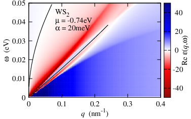
The real part of the dielectric function at a fixed frequency is shown in Fig. 2 where the red line shows the approximation by Eq. (6) and the black line is the full numerical evaluation of Eq. (5). There is always a root of the dielectric function in the limit in which case Eq. (7) reads
The solution corresponds to the plasmon mode with the dispersion given by , where
A second root of Eq. (7) may exist in the range of frequencies given by
where is an analog of Thomas-Fermi wavenumber for each of the spin/valley species. In order for the second root to exist the dielectric function has to become positive
| (8) |
within . The condition in Eq. (8) in the long wavelength limit, , is satisfied so long as
In the lowest order in wavenumber a divergence appears in the dielectric function
| (9) |
which guarantees the existence of the second root. However, at larger wavenumbers the divergence in Eq. (9) is rounded off and the second root of the dielectric function disappears. This is reflected by the termination of the linear branch of the plasmon dispersion shown in solid black lines in Fig. 1(a,b). At high hole doping the difference in Fermi velocities becomes relatively small and the linear mode disappears.

The variation of the plasmon spectrum with the chemical potential is shown in Figure 3(a). When is located in only the -spin/-valley band (orange line, , ), the second mode is absent. When the -spin/-valley band becomes occupied (blue line, , ) the second mode becomes active. Initially, the range of momenta for which the second mode exists is small and grows as moves deeper into the -spin/-valley band (green line, , ). However, as the chemical potential increases further (red line, , ), the range of wave vectors where the second mode exists starts to decrease, and eventually the second mode vanishes (black line, , ).
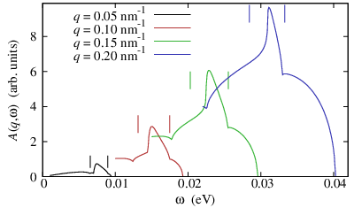
The first plasmon mode is not affected by Landau damping, which is limited to the frequency range . However, the second mode is subject to Landau damping due to electron-hole excitations allowed in the -spin/-valley band. To illustrate the stability of the second plasmon mode, in Fig. 4 we plot the spectral function associated with the plasmon propagator
as a function of for different . The quasiparticle peak is well defined at all wave vectors, and is located between the onset of the two continua, in the narrow region of frequencies between the two electron-hole excitation thresholds of -spin and -spin bands, , respectively. The line shape of the quasiparticle peak corresponding to is distinct from a regular Lorentzian, which reflects Fano-like suppression of the spectral weight due to mixing of plasmons with the electron-hole excitation continuum. The strength of the response from the continuum grows with , but the height of the quasiparticle peak above the continuum increases slightly. The width of the quasiparticle peak also decreases with increasing . Note that the ratio of the peak maximum to the background of the spectral function is consistent with the real and imaginary parts of the dynamical dielectric function being of the same order, in which case this ratio is roughly equal to 2. This indicates that the additional quasiparticle peak identified here is a generic property of a 2D electron gas with lifted spin degeneracy.
With regard to the possibility to observe the predicted splitting of the plasmon spectrum in TMDs experimentally, a crucial parameter is the Zeeman energy. The simplest way to induce strong Zeeman splitting is using magnetic field. The smallest Zeeman field considered in our quantitative calculation, , corresponds to a very high but experimentally accessible magnetic field of (assuming -factor for an out-of-plane field [28]). At such high fields Hall quantization is possible resulting in a discrete spectrum in contrast to the continuous case considered here. In this case the plasmon spectrum is modified due to mixing with cyclotron modes. The splitting of the spectrum predicted here will persist and will be observable in presence of Landau quantization. This situation deserves a separate detailed study. Rotating the magnetic field so that it is in the plane of the TMD removes the Landau quantization, but the anisotropy of the -factor means that a stronger magnetic field is required to achieve a Zeeman field of . An alternative way to achieve very large Zeeman fields (without Hall quantization) is using the proximity effect with a magnetic insulator. Recently, a proximity induced Zeeman field was demonstrated in heterostructures with a Curie temperature . [30, 31] Alternative magnetic insulators can have much higher Curie temperatures for example was reported recently for strained ultra-thin ( unit cells) film on a substrate,[32] and of a layered anti-ferromagnet . [33]
In conclusion, we analyzed the evolution of the plasmon spectrum TMDs in the presence of a strong Zeeman field as a function of the chemical potential. We find that in a wide range of parameters there appears a second plasmon mode characterized by almost linear in wavenumber dispersion. This additional mode is subject to the effect of Landau damping. However, the damping is relatively weak and the mode is associated with a pronounced quasiparticle peak in the spectral function of the electron gas. The shape of the plasmon peak in the spectral function is distinctly non-Lorentzian and reflects the mixing of the mode with electron-hole excitations. The predicted splitting in the collective excitation spectrum is a clear signature of a strong Zeeman field and may be used to identify proximity effect in a TMD/ferromagnetic insulator heterostructure.
Acknowledgements.
We would like to thank Sankar Das Sarma and Euyheon Hwang for helpful discussions. This work is supported by CMTC-LPS-NSA and US-ONR-MURI.References
- [1] A. K. Geim and I. V. Grigorieva, Nature 499, 419 (2013).
- [2] R. A. Gordon, D. Yang, E. D. Crozier, D. T. Jiang, and R. F. Frindt, Physical Review B 65, 125407 (2002).
- [3] Q. H. Wang, K. Kalantar-Zadeh, A. Kis, J. N. Coleman, and M. S. Strano, Nature Nanotechnology 7, 699 (2012).
- [4] B. Radisavljevic, A. Radenovic, J. Brivio, V. Giacometti, and A. Kis, Nature Nanotechnology 6, 147 (2011).
- [5] A. N. Grigorenko, M. Polini, and K. S. Novoselov, Nature Photonics 6, 749 (2012).
- [6] Y. Liu, R. F. Willis, K. V. Emtsev, and T. Seyller, Physical Review B 78, 201403 (2008).
- [7] J. H. Strait, P. S. Nene, W.-M. Chan, C. Manolatou, J. W. Kevek, S. Tiwari, P. L. McEuen, and F. Rana, arXiv:1302.5972 (2013).
- [8] Z. Fei, A. S. Rodin, G. O. Andreev, W. Bao, A. S. McLeod, M. Wagner, L. M. Zhang, Z. Zhao, M. Thiemens, G. Dominguez, M. M. Fogler, A. H. C. Neto, C. N. Lau, F. Keilmann, and D. N. Basov, Nature 487, 82 (2012).
- [9] P. D. Pietro, M. Ortolani, O. Limaj, A. D. Gaspare, V. Giliberti, F. Giorgianni, M. Brahlek, N. Bansal, N. Koirala, S. Oh, P. Calvani, and S. Lupi, Nature Nanotechnology 8, 556 (2013).
- [10] E. H. Hwang and S. Das Sarma, Physical Review B 75, 205418 (2007).
- [11] E. H. Hwang and S. Das Sarma, Physical Review B 80, 205405 (2009).
- [12] R. Sensarma, E. H. Hwang, and S. Das Sarma, Physical Review B 82, 195428 (2010).
- [13] S. Gangadharaiah, A. M. Farid, and E. G. Mishchenko, Physical Review Letters 100, 166802 (2008).
- [14] B. Wunsch, T. Stauber, F. Sols, and F. Guinea, New Journal of Physics 8, 318 (2006).
- [15] A. Scholz, T. Stauber, and J. Schliemann, arXiv:1306.1666 (2013).
- [16] G. Dresselhaus, Physical Review 100, 580 (1955).
- [17] K. F. Mak, K. He, J. Shan, and T. F. Heinz, Nature Nanotechnology 7, 494 (2012).
- [18] T. Cao, G. Wang, W. Han, H. Ye, C. Zhu, J. Shi, Q. Niu, P. Tan, E. Wang, B. Liu, and J. Feng, Nature Communications 3, 887 (2012).
- [19] H. Zeng, J. Dai, W. Yao, D. Xiao, and X. Cui, Nature Nanotechnology 7, 490 (2012).
- [20] D. Xiao, G.-B. Liu, W. Feng, X. Xu, and W. Yao, Physical Review Letters 108, 196802 (2012).
- [21] H. Ochoa, F. Guinea, and V. I. Fal’ko, arXiv:1308.0928 (2013).
- [22] M. Z. Hasan and C. L. Kane, Reviews of Modern Physics 82, 3045 (2010).
- [23] S. Das Sarma and A. Madhukar, Physical Review B 23, 805 (1981).
- [24] G. E. Santoro and G. F. Giuliani, Physical Review B 37, 937 (1988).
- [25] R. E. V. Profumo, R. Asgari, M. Polini, and A. H. MacDonald, Physical Review B 85, 085443 (2012).
- [26] M. Pisarra, A. Sindona, P. Riccardi, V. M. Silkin, and J. M. Pitarke, arXiv:1306.6273 (2013).
- [27] E. Cappelluti, R. Roldan, J. A. Silva-Guillen, P. Ordejon, and F. Guinea, arXiv:1304.4831 (2013).
- [28] H. Rostami, A. G. Moghaddam, and R. Asgari, Physical Review B 88, 085440 (2013).
- [29] A. Kormanyos, V. Zolyomi, N. D. Drummond, P. Rakyta, G. Burkard, and V. I. Falko, Physical Review B 88, 045416 (2013).
- [30] P. Wei, F. Katmis, B. A. Assaf, H. Steinberg, P. Jarillo-Herrero, D. Heiman, and J. S. Moodera, Physical Review Letters 110, 186807 (2013).
- [31] Q. I. Yang and et. al., arXiv:1306.2038 (2013).
- [32] H. Boschker, J. Kautz, E. P. Houwman, W. Siemons, D. H. A. Blank, M. Huijben, G. Koster, A. Vailionis, and G. Rijnders, Physical Review Letters 109, 157207 (2012).
- [33] K. Walther, Solid State Communications 5, 399 (1967).