Electric Field Control of Soliton Motion and Stacking in Trilayer Graphene
Abstract
The crystal structure of a material plays an important role in determining its electronic properties. Changing from one crystal structure to another involves a phase transition which is usually controlled by a state variable such as temperature or pressure. In the case of trilayer graphene, there are two common stacking configurations (Bernal and rhombohedral) which exhibit very different electronic properties [1, 2, 3, 4, 5, 6, 7, 8, 9, 10, 11]. In graphene flakes with both stacking configurations, the region between them consists of a localized strain soliton where the carbon atoms of one graphene layer shift by the carbon-carbon bond distance [12, 13, 14, 16, 17, 18, 15]. Here we show the ability to move this strain soliton with a perpendicular electric field and hence control the stacking configuration of trilayer graphene with only an external voltage. Moreover, we find that the free energy difference between the two stacking configurations scales quadratically with electric field, and thus rhombohedral stacking is favored as the electric field increases. This ability to control the stacking order in graphene opens the way to novel devices which combine structural and electrical properties.
Multilayer graphene has attracted interest in large part due to the ability to induce a sizable band gap with the application of an electric field. The exact nature of the electronic properties of multilayer graphene is controlled both by the number of layers as well as their stacking configuration. The equilibrium in-plane crystal structure of graphene is hexagonal [19], and deviations from this equilibrium require a large amount of energy. Upon stacking multiple graphene sheets, Bernal-stacking – where the A-sublattice of one layer resides above the B-sublattice of the other layer – represents the lowest energy stacking configuration. Thus under normal circumstances, any two graphene layers in a graphite stack will be Bernal-stacked with respect to one another. However, when examining layers more than one apart, there can be multiple nearly-degenerate stacking configurations ( such configurations for n layers) [1]. For example, in the simplest case of trilayer graphene, the top layer may lie directly above the bottom layer (denoted Bernal- or ABA-stacked), or may instead be configured such that one sublattice of the top layer lies above the center of the hexagon of the bottom layer (denoted rhombohedrally- or ABC-stacked). Applying a perpendicular electric field breaks the sublattice symmetry differently depending on the stacking configuration, and thus is capable of re-ordering the energy hierarchy of the stacking configurations [1, 2, 3, 4, 5, 6, 7, 8, 9, 10, 11]. As a consequence, multilayer graphene exhibits the rare behavior of crystal structure modification, and hence modification of electronic properties, via the application of an external electric field.
To examine this effect, we perform scanning tunneling topography (STM) and scanning tunneling spectroscopy (STS) measurements of trilayer graphene on hexagonal boron nitride (hBN). Fig. 1(a) shows a schematic of our experimental setup with the STM tip and the electrical connections indicated. Fig. 1(b) shows Raman spectroscopy mapping of the graphene on hBN flake measured in this study. A central region of trilayer graphene is surrounded by a bilayer region below and a tetralayer region above. The left side of the trilayer region is ABA-stacked and the right side is ABC-stacked. These regions are identified by a change in the width of the Raman 2D peak [20, 21]. A smooth transition of the stacking order can be achieved via a domain wall with a localized region of strain (a strain soliton), where one layer shifts by the carbon-carbon spacing, Å [12, 13, 14, 16, 17, 18, 15]. The interface lies above a flat region of hBN, is atomically smooth in STM topography measurements, and does not display a sizable moiré pattern [22]; therefore it is a good candidate for the study of the intrinsic physics of the domain wall. The ends of the domain wall are bounded by the bilayer and tetralayer regions.

An STM tip is used to scan across the domain wall separating the ABA- and ABC-stacked trilayer graphene regions. There is a net electric field in the region underneath the tip created by voltage differences between the STM tip, silicon back gate and graphene. Figs. 1(c) and (d) show normalized (dI/dV)/(I/V) spectroscopy as a function of gate voltage for the ABA and ABC stacking orders respectively, taken far from the domain wall. The results are similar to those seen in trilayer graphene on SiO2 [23]. Most importantly, the ABA region remains metallic for all gate voltages probed. In contrast, a sizable band gap can be opened in the ABC region with the application of large gate voltages. The spectroscopy for the two stacking orders is easily distinguishable for all gate voltages, even within a few nanometers of the domain wall separating the two stacking orders. This permits very accurate determination of the domain wall location using spectroscopy measurements.
To investigate the connection between the position of the domain wall and the electronic properties of trilayer graphene, we perform dI/dV spectroscopy as a function of tip position scanning from the ABA to ABC region. Figs. 2(a) and (b) show two examples of these measurements (normalized by I/V), taken at different locations on the soliton and at large negative gate voltages (where there is a large gap in the ABC trilayer region). Fig. 2(a) is taken within a few hundred nanometers of the bilayer edge. In this case, the spectroscopy smoothly evolves from ABA to ABC over a spatial extent of about 20 nm. Fig. 2(b) is taken closer to the center of the trilayer region. In this case, the spectroscopy abruptly changes from ABA to ABC. In this region of the sample, even maps with atomic resolution show an abrupt transition from ABA to ABC. As we argue below, this peculiar behavior is due to the STM tip dragging the domain wall for a finite distance along the sample before it snaps back to its equilibrium position. For the case of Fig. 2(a), the STM tip is very close to the pinned boundary (the bilayer edge) and therefore the energy cost of moving the domain wall is too large to overcome.
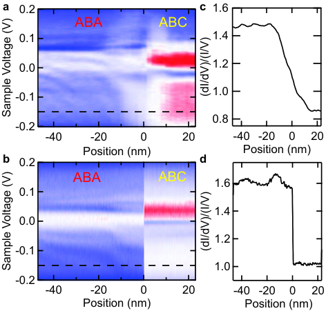
To understand the behavior of the domain wall we take a line cut of the spectroscopy across the boundary at a fixed sample voltage of -150 mV. Figures 2(c) and (d) show the results for the smooth and abrupt transitions, respectively. In both cases, the transition from ABA to ABC stacking can be clearly observed at all sample voltages. Figure 3(a) shows similar line cuts of dI/dV spectroscopy as a function of gate voltage (and therefore electric field) for the pinned domain wall. The red (yellow) region corresponds to ABA (ABC) stacking. We find there is little to no movement of the domain wall in the pinned region as the electric field changes. However, similar measurements near the center of the trilayer region, where the abrupt transition is observed, show markedly different behavior as a function of gate voltage. Fig. 3(b) shows the comparable measurement to Fig. 3(a) in the unpinned region. Here, we find that the position of the domain wall remains nearly stable at small gate voltages, but can change by more than 100 nm with the application of large gate voltages. As the gate voltage (and electric field) becomes larger, more of the sample becomes ABC stacked.

The movement of the ABA/ABC interface can be understood from the energetics of the domain wall. In the absence of an external STM tip, the domain wall position is determined by pinning, elastic energy and stacking energy (see Supplementary Information for details). Assuming that stacking shifts occur only parallel to one of the lattice vectors, we obtain a soliton-like profile of the domain wall with a width ranging from nm for a shear soliton with shifts parallel to the domain wall to nm for a tensile soliton with shifts perpendicular to the domain wall. The external STM tip introduces three additional ingredients; an elastic energy for displacing the soliton from its equilibrium position, a repulsive van der Waals potential between the tip and soliton, and an energy imbalance between the ABA and ABC regions under a perpendicular electric field. The elastic potential for pulling the soliton of length away from a point (where is the relative position) a distance is quadratic in , for , with eV/nm. The van der Waals interaction is given by , where eV nm2 is the repulsion strength, is the radius of curvature of the tip, is the tip-sample distance, and is the tip position. An electric field opens a gap in the ABC region but not in the ABA region which creates a difference in electronic energy [6] that depends on the location of the tip. The induced energy imbalance may be parametrised by a coefficient as where the electric field is computed assuming a spherical tip above the silicon back gate. The integral is taken only over the ABC region ().
Putting all these ingredients together, we obtain the total potential energy of the soliton,
| (1) |
The equilibrium soliton displacement is determined by following the local minimum of the potential [] as the tip position is adiabatically swept. This displacement depends on the tip scan direction and the electric field . It exhibits instabilities beyond certain snapping thresholds, which represent the maximum soliton displacements in a given scan. Scanning from the ABC side towards the ABA side (Figs. 4(a) and (b)), the tip repels the soliton, which is stretched much like a rubber band. The repulsion is the sum of van der Waals plus the electronic contribution from opening a gap in the ABC region. When the elastic force from stretching the soliton equals this repulsion, the soliton cannot be pushed further. As the tip continues to move beyond this point, the soliton snaps back towards its original location and the spectroscopy abruptly changes to ABA graphene. Scanning in the opposite direction (Figs. 4(c) and (d)), the picture is similar, but the electronic contribution is attractive instead of repulsive, and tends to counter the van der Waals repulsion. Hence, the soliton jumps at smaller maximum displacements. In either case, as the soliton jumps under the tip, the measured spectroscopy abruptly changes between ABA- and ABC-type.

The rightward-pointing markers in Fig. 4(e) map out the experimentally found threshold position as the tip scans from the ABA region into the ABC region, as determined by the location where the topographic signal changes. These positions are in agreement with the abrupt changes in the dI/dV spectroscopy observed in Fig. 3(b). The leftward-pointing markers in Fig. 4(e) correspond to the opposite scan direction, starting in ABC and moving towards ABA. The data in both directions can be well fit with our model (solid lines). Parameters eV/nm and eV nm2 in our description are predicted by theory, while is determined by Raman spectroscopy and nm is based on scanning electron microscope images of similar tips. The tip-sample distance nm is set by the tunneling parameters and the traction point is based on the location of the tip. The last parameter, is constrained by theory to a narrow window (see Supplementary Information). From our fits, we obtain . As a check for our model, we have repeated the measurement on a different region of the soliton with a second, similar tip. We find that we can fit this tip’s data by only slightly changing the parameters associated with the tip and the traction point (see Supplementary Information).
As with a local electric field created by an STM tip, a global electric field will also move stacking solitons to increase the ABC-stacked area of the device. This suggests novel and exciting devices that exploit the tunable location of the stacking boundary. As an example, the soliton may be initially placed underneath one of the source-drain contacts such that the entire conduction path for charge carriers in the device is ABA-stacked. With the application of a large enough electric field, the soliton will snap into the ABA region, making the device ABC-stacked and gapped, thus quickly turning off conduction in the device. Such a device would be a good candidate for a graphene FET, offering rapid on-off switching with a high on-off resistivity ratio resulting from the difference in conductivity between ungapped ABA- and gapped ABC-stacked trilayer graphene.
Methods
Mechanically exfoliated multilayer graphene was transferred onto high quality single crystals of hBN which were mechanically exfoliated on a SiO2 substrate [24]. Flakes were characterized via Raman spectroscopy with a WITec Alpha 300RA system using the 532 nm line of a frequency-doubled Nd:YAG laser as the excitation source. The spectra were measured in the backscattering configuration using a 100x objective and either a 600 or 1800 grooves/mm grating. After depositing the graphene on hBN, Cr/Au electrodes were written using electron beam lithography. The devices were annealed at 350∘C for 2 hours in a mixture of Argon and Hydrogen and then at 300∘C for 1 hour in air before being transferred to the UHV LT-STM for topographic and spectroscopic measurements.
All the measurements were performed in UHV at a temperature of 4.5 K. dI/dV measurements were acquired by turning off the feedback circuit and adding a small (5 mV) ac voltage at 563 Hz to the sample voltage. The current was measured by lock-in detection.
Acknowledgements
P.S.-J. acknowledges fruitful discussions with J. F. Rossier.
M.Y. and B.J.L. were supported by the U. S. Army Research Laboratory and the U. S. Army Research Office under contract/grant number W911NF-09-1-0333. J.I-J.W. was partially supported by a Taiwan Merit Scholarship TMS-094-1-A-001. J.I-J.W and P.J-H. have been primarily supported by the US DOE, BES Office, Division of Materials Sciences and Engineering under Award DE-SC0001819. Early fabrication feasibility studies were supported by NSF Career Award No. DMR-0845287 and the ONR GATE MURI. This work made use of the MRSEC Shared Experimental Facilities supported by NSF under award No. DMR-0819762 and of Harvard’s CNS, supported by NSF under grant No. ECS-0335765. A.G.B. was supported by the U.S. Army Research Laboratory (ARL) Director’s Strategic Initiative program on interfaces in stacked 2D atomic layered materials. P.S.-J. received financial support from the Spanish Ministry of Economy (MINECO) through Grant no. FIS2011-23713, the European Research Council Advanced Grant (contract 290846) and from the European Commission under the Graphene Flagship (contract CNECT-ICT-604391).
Supplementary Information
In this Supplementary Material we present our model for the energetics of a stacking soliton at the interface between ABA- and ABC-stacked trilayer graphene. We first consider the elastic energy of a free, relaxed soliton in Sect. I, and how this energy grows under traction in Sect. II. We then describe in Sect. III how an electric field affects differently the electronic free energy in ABA- and ABC-stacked trilayer graphene. In particular, it opens a gap in the electronic spectrum in the case of ABC- but not ABA-stacking, which results in a lower free energy per unit area in the former with respect to the latter. We show that this energy difference scales as . In Sect. IV we describe the profile of produced by an idealized tip. In Sect. V we model the short ranged van der Waals force between the tip and the soliton, which is present regardless of the backgate potential. In Sect. VI we describe how to compute the hysteretic evolution of the soliton, in the presence of the elastic, electric and van der Waals forces, as the STM tip scans through its relaxed position in either the ABA-to-ABC or ABC-to-ABA directions. Finally, in Sect. VII we show data and fits for a second tip.
I Elastic description of a relaxed soliton
In this section we derive, from elasticity theory, the spatial profile, characteristic width and energy density of a relaxed stacking soliton in a graphene bilayer. This description also applies to an ABC/ABA trilayer soliton, assuming that the bottom layer is not strained.
A stacking soliton in a graphene bilayer is a domain wall between an AB- and a BA-stacked region, here taken as and respectively. A soliton is defined by a interlayer (2D) vector displacement field , with boundary conditions
| (2) | |||||
| (3) |
corresponding to AB and BA stacking asymptotics. Here, denotes the “flavour” of the soliton, and are the three bond vectors in the uppermost layer, which is the one we will be deforming (we leave the bottom layer fixed for simplicity, without lack of generality). (Note that displacing the top layer of an AB bilayer by a vector transforms it into a BA)
Our aim here is to compute the field that minimizes the total energy , which is the sum of the elastic energy of the deformed top layer,
| (4) | |||||
| (5) |
plus the stacking energy
| (6) |
This stacking energy is derived from the energy cost of different uniform stackings per unit area, . A uniform AB and BA have minimum stacking energy []. Any other stacking has more energy. By incorporating into the total soliton energy, we may arrive at a non-rectilinear soliton profile. Otherwise, the equilibrium soliton has infinite width, to minimize strain in . Below, we will also include the non-uniform stacking energetics, i.e. the full interlayer shear containing also gradients of , to see how the solution is modified.
Our model for must exhibit the same hexagonal symmetry as the lattice. We will assume is very large, except along the three crystallographic . The cut along these directions takes the form
Since any other displacement than the above is energetically prohibitive, this will impose a constraint for the possible soliton displacement fields,
where must be determined, and describes the soliton profile in space. Its boundary conditions are
| (7) | |||||
| (8) |
We constrain our soliton ansatz further, by assuming it is a straight ridge, oriented at an angle respect . Hence
where is the unit vector normal to the soliton. For concreteness we assume, without loss of generality, that the chosen interlayer shift is , where nm is the carbon-carbon bond length. Then, we write
The strain tensor of this soliton reads,
The associated elastic energy reads
where is the monolayer bulk modulus, while is half its shear modulus. Note that for a given profile , the energy of the soliton is mimimum for an orientation (i.e. a “shear” soliton), and maximum for (a “tensile” soliton).
We now define coordinates across () and along () the soliton. The profile is obtained by the minimization of the total energy . The energy density is independent of , so its integral just gives the length of the soliton. Hence we are left with
| (9) |
A convenient single-parameter model for that preserves all relevant symmetries is , with
and [25].
We can now recast Eq. (9) in a dimensionless form,
| (10) |
where
| (11) |
is a lengthscale associated to the half-width of the soliton. We obtain nm for a shear soliton, and nm for a tensile soliton, in agreement with experiments [15].
The solutions that minimize Eq. (10) for different satisfy a scaling invariance , for some universal function , so that changing parameter (for example, adjusting or ) just rescales the spread of the relaxed soliton, but not its shape. The function can be computed numerically, and is shown in Fig. 5. We see that indeed, is roughly the typical half-width of the soliton. The full width then ranges from 12.2 nm (tensile) to 19.0 nm (shear), in good agreement with experimentally measured values (note that this are roughly twice the full-width-half-maximum values, see Fig. 5).
The energy of the soliton solution is
| (12) |
which equates to an energy per unit length
| (13) |
or approximately for a shear soliton, and for a tensile soliton. We see that a tensile soliton has a more energy per unit length than a shear soliton.
II Energy of a soliton under traction
We next consider the energetics of a stretched soliton pulled away perpendicularly to its equilibrium direction by a point like an elastic band. We can generalize the result for a straight soliton Eq. (13) to a curved soliton whose radius of curvature is everywhere larger than its width . Then we may approximate
| (14) |
with and . Here is the local orientation of the soliton at each point.
In the absence of external traction, the equilibrium shape of the soliton will be a straight line, with an orientation everywhere (shear soliton). Assume this is a vertical straight line at . If we pull from the center point at a distance away from , the soliton shape will be some function , such that and . The soliton profile minimizes the total energy. From Eq. (14) we have
| (15) | |||||
| (16) |
The Euler-Lagrange equation for this variational problem is very simple, . Hence, the pulled soliton will remain a straight line to left and right of the pulling point. If the original soliton had a total length , then , and the total energy becomes
| (17) |
Note that is the total energy of the unpulled soliton. The energy ratio between pulled and unpulled solitons is plotted in Fig. 6. If the pull distance is much smaller than the soliton length , the work done by pulling can be approximated by
| (18) |
This equation corresponds to pulling a shear soliton from its center, at . If the pulling point is generic, at , where , and the unpulled soliton is also generic (angle ) , the above equation generalizes to
| (19) |
For a shear soliton, . For a tensile soliton, .
All the above assumes identical energy stacking densities for the AB [] and BA [] sides of the soliton, i.e. . While this symmetry is guaranteed by inversion symmetry in a suspended graphene bilayer, it may be broken in a trilayer. In such a system, the ABA stacking energy density has been calculated [26, 27] to be slightly lower (more stable) than for ABC stacking (). The relaxed configuration of a soliton pinned at two sites a distance apart is no longer a straight line, but becomes bulged towards the ABC side, to minimize the total energy. For realistic parameters, this energy minimum has a curvature, as a function of traction distance around this bulged configuration, that is almost the same as in the case without the ABA/ABC imbalance. We will therefore employ the analytic result Eq. (19) also for a trilayer soliton.
III Energetics of graphene trilayer in an electric field
We next consider the energy balance between ABA- and ABC-stacked trilayer graphene in the presence of an electric field. Such an electric field arises from the potential energy difference between the sample and an STM tip or a backgate, or both. Without field, Ref. [26] explains the dominant ABA stacking in graphite by the presence of a stacking potential favoring ABA over ABC. ABC is however more sensitive to a perpendicular electric field in that the latter opens a gap in its electronic spectrum, while at physically relevant field strengths, there is no gap for ABA stacking [6]. For massive two-dimensional Dirac fermions with dispersion , it is a straightforward exercise to show that, at half filling and low temperature, the difference in free energy between ungapped () and gapped phase is favoring the gapped phase, with the sample’s area . It is therefore expected that in the presence of an electric field, the electronic contribution to the free energy favors ABC stacking over ABA stacking.
To confirm this expectation, we use the low-energy tight-binding Hamiltonians of Refs. [5, 6] for ABA and ABC stackings. Energy levels are obtained by exact diagonalization and the Gibbs free energy is calculated as for both ABA and ABC Hamiltonians, as a function of the electric field in the graphene trilayer. The latter is incorporated as an on-site energy potential in the top layer and in the bottom layer, with the interlayer spacing Å. Following Ref. [8], we take that charge screening in the trilayer reduces the externally applied electric field by a factor of , . The geometry of the experiment gives an estimate of V/Å in the experiments, so that the range of interest is roughly V/Å.
Fig. 7 shows the free energy difference, , per atom between ABA- and ABC-stacked trilayer graphene for different chemical potentials, . The dependence is quadratic in the field and systematically favors the ABC phase. Because the free energy is extensive we write , where we converted the electric field from internal to external. Taking into account screening [8] and for chemical potentials of experimental interest, eV, we extract from this quadratic behavior (eV)-1. The parameter depends on , which in turn varies slightly with tip and backgate voltages. For the sake of simplicity, and because evaluating the experimental value of vs. gate voltage would introduce an additional parameter in the theory, we will neglect this latter dependence in our theoretical discussion of the soliton motion, and instead consider the bound on we just extracted.
IV Electric field profile under a tip
A voltage bias applied between the backgate and the tip gives rise to an electric field on the sample. In this section we compute this profile, assuming the tip may be modelled by a sphere of radius .
Consider the setup sketched in Fig. 8. The sample is sitting on top of a substrate, composed of a nm-thick hexagonal Boron Nitride (hBN) crystal immediately under the sample, plus a nm-thick layer of SiO2 below. Both materials have similar dielectric properties, so they will enter the electrostatic problem as a single slab of thickness nm with dielectric constant . Below it, the backgate is modelled as a flat and infinite metallic plate. The STM tip hovers a distance nm above the sample, which has a thickness nm. The STM tip’s radius of curvature is much larger than . Hence, for the purpose of computing the field produced on the sample, it is reasonable to model the tip as a sphere of radius . Because the sample is very thin we assume that it is transparent and ignore its presence when computing , beyond inducing screening of the electric field as discussed above. The problem then reduces to that of a sphere-plate capacitor, see e.g. Ref. 28. The solution takes the form of a set of point charges and at positions and , where the origin is chosen on the backgate, and the center of the tip is at . These charges satisfy the recurrence
The seed position is given by geometry, and seed charge is fixed by the voltage between the tip and the backgate. Each virtual charge gives a contribution to the field on the sample, which summed up as
This expression allows us to compute the energy gain in ABC, with respect to ABA, in the presence of , using , as discussed in Sect. III. The number of required images grows with the ratio . For the fits in Fig. 4e of the main text, which has nm, we have employed 6 images.

V Van der Waals force between tip and sample
London-Van der Waals forces are important players in scanning microscopy, due to the extreme proximity between bulky tips and the sample. The origin of this force is the attraction between instantaneous dipole moments in each of the two bodies. Each pair of dipoles, separated a distance , contributes with an extremely short range potential that is proportional to the mass density in the sample and the tip, , where is London’s constant. Integrating over a spherical tip of radius that hovers at a distance over the sample (see Fig. 8), we get an attractive potential with respect to a generic point at a distance from the center of the sphere [29]
If we integrate this over all points in a uniform sample of thickness , we obtain the van der Waals attraction between a sphere and a thin plane. The effective van der Waals interaction between the tip and soliton is computed by taking into account that a soliton of width is expected to have a smaller mass density than the uniform trilayer. The density difference may be estimated as , where nm is the Bravais lattice constant, and the soliton width is nm. It is assumed that only the top layer is strained.
The difference in van der Waals energy between a trilayer with a soliton, at a distance from the tip, and that of a uniform trilayer, is given by
where the integral over sample thickness nm and soliton width nm has been approximated in the limit small and . The integral over the coordinate may be evaluated to finally yield
where , and eV is the Hamaker constant [29]. This yields eV nm2. Note that the resulting van der Waals potential between tip and soliton is repulsive, since the mass density difference is negative.
VI Soliton evolution under STM scan
In this section we discuss the behavior of the soliton as the STM tip is scanned across the sample in the presence of an arbitrary tip-backgate bias. At each tip position it exerts a certain force on the soliton, assumed to lie along the axis in quilibrium. The main source of this tip-soliton interaction comes from the electric field under the tip when the backgate voltage . The resulting electric field (Sect. IV) creates an electronic energy imbalance between ABC and ABA (Sect. III)
As a consequence, the tip will repel the soliton when it approaches from the ABC side, but will attract it when coming from the ABA side. The force is proportional to the square of the backgate voltage . The value of , computed in Sect. III, was found to lie within the range .
The soliton is also subject to the elastic recovery force (Sect. II)
where is the soliton displacement, is its total length, is the traction point and eV/nm.
Our measurements show, however, that an additional interaction between tip and soliton exists even without a tip-backgate voltage , as is clear from the fact that abrupt snapping is observed in the differential conductance for any backgate voltage, including zero. The most natural candidate for this residual force is van der Waals repulsion between the tip and the soliton described in Sect. V. Such an interaction will push the soliton even for . Note that other types of interactions [30] could also play a role, but we find that the simple van der Waals model derived in Sect. V
is able to correctly reproduce the experimental results. The coupling constant is eV nm2.
The total energy is thus . To determine the evolution of the soliton displacement under an adiabatic sweep of the tip position , we compute the equilibrium points, defined by for different . These are represented in Fig. 9 for different values of . At (no electronic contribution , black line), we find that the non-linearity of the model, introduced in particular by the repulsion, yields a bistable region for a range of positions , corresponding to a displaced soliton behind and in front of the advancing tip. This bistable region ends at snapping thresholds nm (the range of the van der Waals repulsion), where the repelled soliton in front of the tip is too stretched to be pushed further, and snaps behind the tip (arrows in Fig. 9). The snapping threshold for opposite scan directions is equal and of opposite sign for . This represents a hysteretic soliton displacement. At finite , the above picture is very similar, but the two hysteretic snapping thresholds are pushed into the ABA region as due to the contribution. The fact that the electronic contribution yields a simple shift is a consequence of the large nm, which controls the range of the potential, as compared to the smaller range nm of the van der Waals repulsion . The described phenomenology is in quantitative agreement with the experimental results, as shown in Fig. 4e of the main text, and Fig. 10 in the next section.
VII Movement of soliton
As a check for our model, we have repeated the measurement of the movement of the soliton as a function of gate voltage for a second tip. Once again, we have measured the locations where the topography (or spectroscopy) changes for the two different scan directions. The soliton moves much less in this region but we still observe the abrupt changes in spectroscopy as a function of position. Fig. 10 plots the locations where there is an abrupt change for both scan directions. We are able to fit this data using the same parameters as the main text except for a change in the traction point to within of the soliton edge, and slightly reducing to 0.3 nm. The change in the traction point is because this set of data was acquired near the bilayer region where the soliton ends and is therefore pinned. The value obtained in this fit for parameter , which governs the free energy difference between ABC and ABA under an electric field, is the same, , as for the first tip. This is a relevant consistency check of our model, as should be a tip-independent property, intrinsic to trilayer graphene.
References
- [1] Aoki, M., and Amawashi, H. Dependence of band structures on stacking and field in layered graphene. Solid State Commun. 142, 123-127 (2007).
- [2] Guinea, F., Castro Neto, A. H., and Peres, N. M. R. Electronic states and Landau levels in graphene stacks. Phys. Rev. B 73, 245426 (2006).
- [3] Avetisyan, A. A., Partoens, B., and Peeters, F. M. Electric field tuning of the band gap in graphene multilayers. Phys. Rev. B 79, 035421 (2009).
- [4] Koshino, M., and McCann, E. Gate-induced interlayer asymmetry in ABA-stacked trilayer graphene. Phys. Rev. B 79, 125443 (2009).
- [5] Avetisyan, A. A., Partoens, B., and Peeters, F. M. Electric-field control of the band gap and Fermi energy in graphene multilayers by top and back gates. Phys. Rev. B 80, 195401 (2009).
- [6] Avetisyan, A. A., Partoens, B., and Peeters, F. M. Stacking order dependent electric field tuning of the band gap in graphene multilayers. Phys. Rev. B 81, 115432 (2010).
- [7] Koshino, M. Interlayer screening effect in graphene multilayers with ABA and ABC stacking. Phys. Rev. B 81, 125304 (2010).
- [8] Zhang, F., Sahu, B., Min, H., and MacDonald, A. H. Band structure of ABC-stacked graphene trilayers. Phys. Rev. B 82, 035409 (2010).
- [9] Kumar, S. B., and Guo, J. Multilayer graphene under vertical electric field. Appl. Phys. Lett. 98, 222101 (2011).
- [10] Wu, B.-R. Field modulation of the electronic structure of trilayer graphene. Appl. Phys. Lett. 98, 263107 (2011).
- [11] Tang, K. et al. Electric-field-induced energy gap in few-layer graphene. J. Phys. Chem. C 115, 9458-9464 (2011).
- [12] Zhang, F., MacDonald, A. H., and Mele, E. J. Valley Chern numbers and boundary modes in gapped bilayer graphene. PNAS 110 10546-10551 (2013).
- [13] Vaezi, A., Liang, Y., Ngai, D. H., Yang, L., and Kim. E.-A. Topological Edge States at a Tilt Boundary in Gated Multilayer Graphene. Phys. Rev. X 3, 021018 (2013).
- [14] San-Jose, P. and Prada, E. Helical networds in twisted bilayer graphene under interlayer bias. Phys. Rev. B 88, 121408 (2013).
- [15] Alden, J. S., et al. Strain solitons and topological defects in bilayer graphene. PNAS 110 11256-11260 (2013).
- [16] Xu, P. et al. A pathway between Bernal and rhombohedral stacked graphene layers with scanning tunneling microscopy. Appl. Phys. Lett. 100, 201601 (2012).
- [17] Warner, J. H., Mukai, M., and Kirkland, A. I. Atomic Structure of ABC Rhombohedral Stacked Trilayer Graphene. ACS Nano 6, 5680-5686 (2012).
- [18] Hattendorf, S., Georgi, A., Liebmann, and Morgenstern, M. Networks of ABA and ABC stacked graphene on mica observed by scanning tunneling microscopy. Surface Science 610, 53-58 (2013).
- [19] Castro Neto, A. H., Guinea, F., Peres, N. M. R., Novoselov, K. S., and Geim, A. K. The electronic properties of graphene. Rev. Mod. Phys. 81, 109-162 (2009).
- [20] Lui, C. H., et al. Imaging stacking order in few-layer graphene. Nano Lett. 11, 164-169 (2011).
- [21] Cong, C., et al. Raman characterization of ABA- and ABC-stacked trilayer graphene ACS Nano 5, 8760 (2011).
- [22] Yankowitz, M., et al. Emergence of superlattice Dirac points in graphene on hexagonal boron nitride. Nature Phys. 8 382-386 (2012).
- [23] Yankowitz, M., Wang, F., Lau, C. N., and LeRoy, B. J. Local spectroscopy of the electrically tunable band gap in trilayer graphene. Phys. Rev. B 87, 165102 (2013).
- [24] Dean, C. R. et al. Boron nitride substrates for high-quality graphene electronics. Nature Nanotech. 5, 722-726 (2010).
- [25] Popov, A. M., Lebedeva, I. V., Knizhnik, A. A., Lozovik, Y. E., and Potapkin, B. V. Commensurate-incommensurate phase transition in bilayer graphene. Phys. Rev. B 84, 045404 (2011).
- [26] Charlier, J.-C., Michenaud, J.-P., and Gonze, X. First-principles study of the electronic properties of simple hexagonal graphite. Phys. Rev. B 46, 4531-4539 (1992).
- [27] Charlier, J.-C., Gonze, X., and Michenaud, J.-P. First-principles study of the stacking effect on the electronic properties of graphite(s). Carbon 32, 289-299 (1994).
- [28] Dall’Agnol, F. F., and Mammana, V. P. Solution for the electric potential distribution produced by sphere-plane electrodes using the method of images. Revista Brasileira de Ensino de Fisica 31, 3503 (2009).
- [29] Hamaker, H. The London—van der Waals attraction between spherical particles. Physica 4, 1058-1072 (1937).
- [30] Saint Jean, M., Hudlet, S., Guthmann, C., and Berger, J. Van der Waals and capacitive forces in atomic force microscopies. Journal of Applied Physics 86, 5245-5248 (1999).