A Tracker for the Mu3e Experiment based on High-Voltage Monolithic Active Pixel Sensors
Abstract
The Mu3e experiment searches for the lepton flavour violating decay , aiming for a branching fraction sensitivity of . This requires an excellent momentum resolution for low energy electrons, high rate capability and a large acceptance. In order to minimize multiple scattering, the amount of material has to be as small as possible. These challenges can be met with a tracker built from high-voltage monolithic active pixel sensors (HV-MAPS), which can be thinned to 50 µm and which incorporate the complete read-out electronics on the sensor chip. To further minimise material, the sensors are supported by a mechanical structure built from 25 m thick Kapton foil and cooled with gaseous helium.
Keywords:
Tracking , Silicon Sensors , Lepton Flavour Violation1 Motivation
In the standard model of elementary particles (SM), lepton flavour is a conserved quantity. In the neutrino sector, lepton flavour violation (LFV) has however been observed in the form of neutrino mixing. Consequently, lepton flavour symmetry is a broken symmetry, the standard model has to be adapted to incorporate massive neutrinos and LFV is also expected in the charged lepton sector, but has so far not been observed. The exact mechanism and size of LFV being unknown, its study is of large interest, as it is linked to neutrino mass generation, CP violation and new physics beyond the SM. In fact, even in a Standard Model extended with massive neutrinos, the branching fraction for decays like is suppressed to unobservable levels of ; an observation would thus be an unequivocal sign for new physics.
The Mu3e experiment [1] aims to find or exclude the decay at the level, improving the last measurement [2] by four orders of magnitude. Performing this measurement within a few years requires very intense, continuous muon beams, which are provided by the high-intensity proton accelerator at the Paul Scherrer Institute (PSI) in Switzerland. Muon stop rates in excess of per second are currently available. A future high-intensity muon beam (HIMB) capturing muons produced in the spallation target of the Swiss neutron source (SINQ) would push this beyond the per second required to reach in branching fraction sensitivity. Running at rates of several billion muon decays per second and at the same time being able to suppress backgrounds by 16 orders of magnitude and being efficient for the signal is a formidable challenge for the detection system.
2 Requirements for the Detector
signal events are constituted by an electron and two positron tracks with a common vertex and coincident in time. As they originate from a muon decay at rest, the vectorial sum of their momenta should vanish and their energies should add up to the muon mass. The maximum momentum is MeV/. There are two main categories of background, on one hand accidental coincidences of positrons from ordinary muon decays with an electron from e.g. photon conversion, Bhabha scattering or mis-reconstruction of positrons curling back in the magnetic field. Accidental backgrounds can be suppressed by excellent vertex, timing and momentum resolution. On the other hand there is the background due to the internal conversion muon decay , which looks exactly like the signal decay, except that the neutrinos carry away some energy and momentum. From the branching fraction as a function of missing energy, the overall energy resolution required for a given sensitivity can be derived, see Fig. 1.
In summary, the Mu3e detector must provide excellent vertex and timing resolution as well as an average momentum resolution better than MeV/ with a large geometrical acceptance and at the same time be capable of standing muon decays per second.
A momentum measurement can be performed by measuring a direction (e.g. with a double layer of detectors) and a third point with some lever arm to determine the curvature in the magnetic field. For the low momentum electrons11 1 From here on meant to imply both electrons and positrons in Mu3e, multiple Coulomb scattering (with expected scattering angle ) and the lever arm are the dominating quantities affecting the resolution, to first order
| (1) |
see Fig. 2a. For good momentum resolution it is thus imperative to have a minimum amount of material, which determines the detector technology as described in section 3 and a large lever arm (ideally close to a semi-circle of the track, where multiple scattering effects cancel to first order, see Fig. 2b), which determines the detector geometry, section 4.
3 Detector Technology
For Mu3e, minimizing the material within the acceptance is crucial. Gas detectors however cannot stand the required rates due to ageing or occupancy (wire chambers) or do not deliver the required precision due to space charge effects (time-projection chambers, see e.g. [6]). Solid state detectors until recently were either too thick (hybrid systems) or too slow (monolithic active pixel sensors, MAPS) for the task at hand. The high-voltage MAPS technology [4, 7, 8] offers a way out of this dilemma by providing sensors that can be thinned to below 50 µm thickness and ran at frame rates above 10 MHz due to fast charge collection and built-in zero-suppression.
The MUPIX series of HV-MAPS are fabricated in a commercial process (AMS 180 nm HV-CMOS) and apply voltages of 50-100 V between the substrate and the deep -wells containing the active electronics (see Fig. 3 for a schematic drawing), leading to the fast charge collection via drift from a thin active depletion zone. The MUPIX 2 prototype with pixels of µm2 size was characterized extensively during 2012 [5, 9]. The chips implement a charge sensitive amplifier and a source follower inside the pixels and a comparator plus digital electronics in the chip periphery. The signal size is measured via the time-over-threshold method. For drift voltages above V signal amplification is observed, see Fig. 4, left. The use of LED flashes to generate signals allows for latency measurements between the flash and the appearance of the signal at the comparator exit. These latencies are of the order of 0.5 µs, dominated by the shaping time and improving with high voltage, see Fig. 4, right. The noise of the sensor was estimated using the sharpness of the threshold for a known injection signal and the signal size estimated using a 55Fe radioactive source, giving signal-to-noise-ratios well above 20.
The MUPIX 3 chip currently under study includes additional digital column logic and encodes hit information encompassing row and column address and a timestamp. Also the pixels are now µm2 in size, close to the µm2 required for the production of and cm2 sensors, which will also include digital logic serializing the hit information on chip and sending it out via up to four 800 Mbit/s low-voltage differential signalling links.
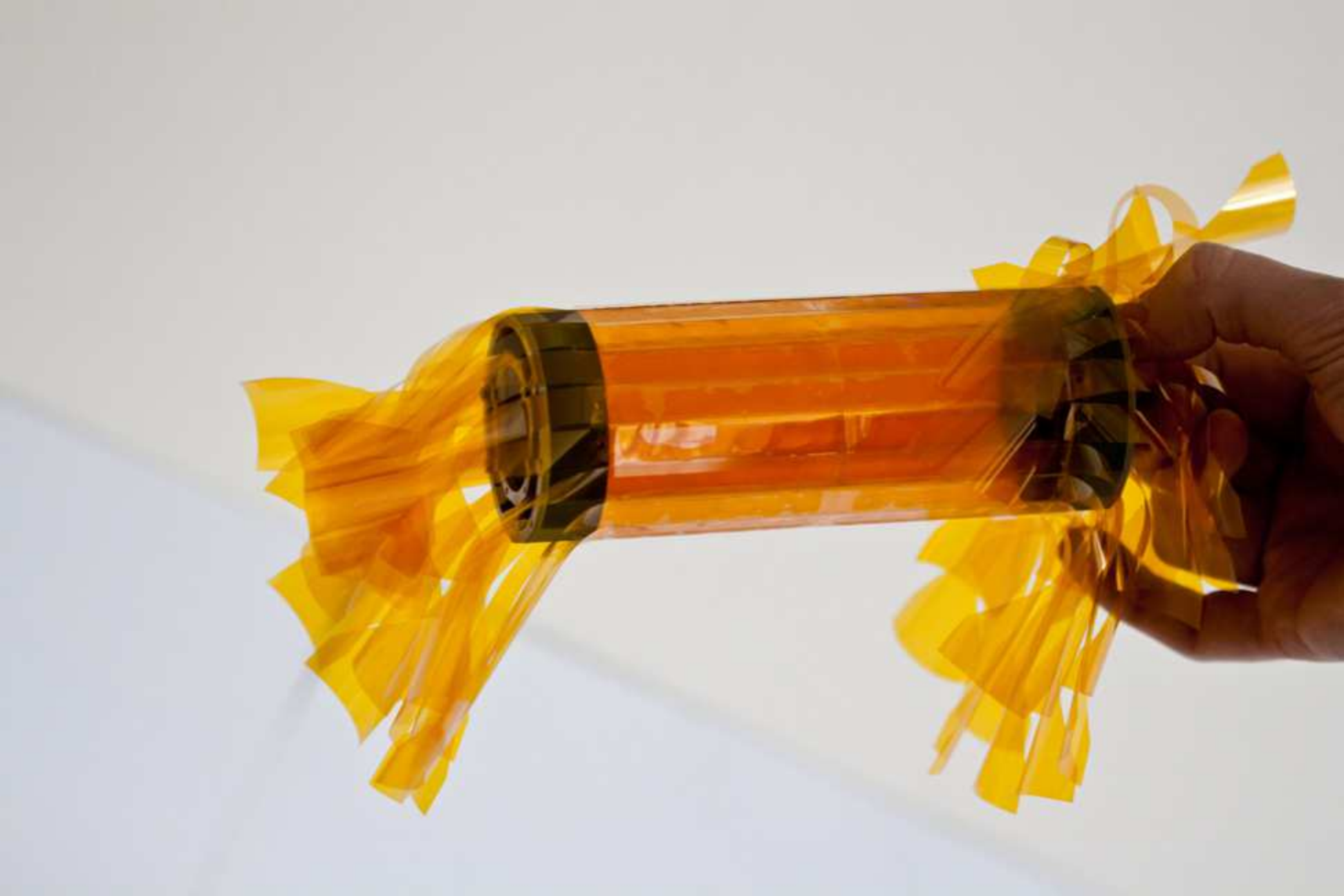
The MUPIX chips will be glued and bonded to Kapton™ flex-prints with aluminium traces for signals and power. These flex-prints in turn are glued to a Kapton™ prism serving as a mechanical support. A complete layer with 50 µm silicon and twice 25 µm Kapton™ plus aluminium and adhesive is less than a permille of a radiation length thick. Prototypes of this mechanical structure using glass plates instead of the silicon have been produced and were found to be surprisingly sturdy (and self-supporting), see Fig. 5. The largest such structures required in the experiment cover 36 cm between supports. In order not to add dead material, the heating power of the chips (estimated at 150 mW/cm2) will be cooled by a flow of gaseous Helium. How to prevent the necessary high flow rates of several m/s [10] from exciting vibrations in the sensor layers is currently under study.
4 Detector Concept
The Mu3e tracking detector should be sensitive for a transverse momentum range from 12 to 53 MeV/ and provide a momentum resolution of better than 0.5 MeV/ over the same range. Moving the detectors to large radii in order to have a large lever arm for high transverse momentum tracks sacrifices acceptance at low momenta (Fig. 6a), whereas at small radii, the lever arm is not sufficient for delivering the required precision at large momenta (Fig. 6b). The Mu3e detector is small, but achieves a large lever arm, often close to the optimum of a semi-circle by also measuring the re-curling part of the track (Fig. 6c). A good solid angle coverage for re-curling tracks leads to a long pipe design for the detector, see Fig. 7. This design encompasses a hollow double-cone muon stopping target, made e.g. from 30 to 80 µm aluminium surrounded by two pixel detector layers for vertex determination. Between the inner and outer pixel detectors, three layers of 250 µm scintillating fibres allow for a timing measurement with resolution. The outer pixel layers and their extension in forward and backward direction allow for precise momentum measurement with re-curling tracks. Inside of the forward and backward extensions, scintillating tiles perform a timing measurement with a resolution better than 100 ps. This overall arrangement of detectors leads to a minimum disturbance of the momentum (and vertex) measurement by the timing detectors, as the main contribution to the momentum resolution comes from the free space curl outside of the detector tube. Another advantage of this design is the modularity, which allows for a staged approach in step with increasing muon rates. A phase Ia detector will consist of only the inner and outer central pixel detectors, sufficient for muon rates of a few 107/s. Phase Ib will add the scintillating fibres and a first set of forward and backward extensions with pixels and tiles and run at 108 muons/s. The full detector as shown in Fig. 7 together with a new beam line providing muons/s will constitute the phase II experiment.
5 Performance Studies
The detector performance is studied both using a Geant4 [11, 12] based simulation with a detailed description of materials and the magnetic field as well as a simplified model mainly for reconstruction studies assuming perfectly cylindrical tracking layers. A three-dimensional multiple scattering track fit ignoring detector resolution is employed for track finding. It is planned to employ a general broken line fit [13, 14, 15] in a second step in order to obtain the best possible resolution. The results presented in the following were obtained with a simplified model and a multiple scattering dominated fit. Fig. 8 shows the momentum resolution for tracks from ordinary muon decays with an RMS of 280 keV/. The resolution for the invariant mass of the three decay particles is shown in Fig. 9. Fig. 10 finally shows the ability of the presented detection system for separating the signal from the background.
6 Conclusions
The Mu3e tracking detector employs a variety of innovative techniques in order to obtain the best possible momentum resolution in a multiple scattering dominated environment, namely:
- 1.
HV-MAPS sensors thinned to 50 µm thickness;
- 2.
A mechanical structure built from 25 µm Kapton™ foil and a 25 µm Kapton™ flexprint, leading to a layer thickness of less than a permille of a radiation length;
- 3.
Cooling with gaseous helium in order not to add material;
- 4.
The use of recurling tracks for increasing the lever arm for momentum measurements.
The combination of these techniques achieves a three particle invariant mass resolution in the order of 0.5 MeV/, thus fulfilling the requirements of the Mu3e experiment for reaching in branching ratio sensitivity for the decay .
Acknowlegments
N. Berger would like to thank the Deutsche Forschungsgemeinschaft for supporting him and the Mu3e project through an Emmy Noether grant. M. Kiehn acknowledges support by the IMPRS-PTFS.
References
- [1] A. Blondel et al., “Research Proposal for an Experiment to Search for the Decay ”, ArXiv e-prints, January 2013, (arXiv:1301.6113 [physics.ins-det]).
- [2] U. Bellgardt et al., [SINDRUM Collaboration], “Search for the Decay ”, Nucl.Phys., B299 1, 1988.
- [3] R. M. Djilkibaev and R. V. Konoplich, “Rare Muon Decay ”, Phys.Rev., D79 073004, 2009, (arXiv:0812.1355 [hep-ph]).
- [4] I. Peric, “A novel monolithic pixelated particle detector implemented in high-voltage CMOS technology”, Nucl.Instrum.Meth., A582 876, 2007.
- [5] A.-K. Perrevoort, Characterisation of High Voltage Monolithic Active Pixel Sensors for the Mu3e Experiment, Master’s thesis, Heidelberg University, 2012.
- [6] F. V. Böhmer, M. Ball, S. Dørheim, C. Höppner, B. Ketzer, I. Konorov, S. Neubert, S. Paul, J. Rauch and M. Vandenbroucke, “Space-Charge Effects in an Ungated GEM-based TPC”, 2012, (arXiv:1209.0482 [physics.ins-det]).
- [7] I. Peric, C. Kreidl and P. Fischer, “Particle pixel detectors in high-voltage CMOS technology - New achievements”, Nucl. Instr. Meth., A 650(1) 158, 2011.
- [8] I. Peric and C. Takacs, “Large monolithic particle pixel-detector in high-voltage CMOS technology”, Nucl. Instrum. Meth., A624(2) 504, 2010.
- [9] H. Augustin, Charakterisierung von HV-MAPS, Bachelor thesis, Heidelberg University, 2012.
- [10] M. Zimmermann, Cooling with Gaseous Helium for the Mu3e Experiment, Bachelor thesis, Heidelberg University, 2012.
- [11] J. Allison, K. Amako, J. Apostolakis, H. Araujo, P.A. Dubois et al., “Geant4 developments and applications”, IEEE Trans. Nucl. Sci., 53 270, 2006.
- [12] S. Agostinelli et al., “Geant4–a simulation toolkit”, Nucl. Instr. Meth., A 506(3) 250 – 303, 2003.
- [13] V. Blobel, C. Kleinwort and F. Meier, “Fast alignment of a complex tracking detector using advanced track models”, Comput.Phys.Commun., 182 1760–1763, 2011, (arXiv:1103.3909 [physics.ins-det]).
- [14] C. Kleinwort, “General Broken Lines as advanced track fitting method”, 2012, (arXiv:1201.4320 [physics.ins-det]).
- [15] M. Kiehn, Track Fitting with Broken Lines for the MU3E Experiment, Diploma thesis, Heidelberg University, 2012.