The Coherent Interlayer Resistance of a Single, Rotated Interface between Two Stacks of AB Graphite
Abstract
The coherent, interlayer resistance of a misoriented, rotated interface between two stacks of AB graphite is determined for a variety of misorientation angles. The quantum-resistance of the ideal AB stack is on the order of 1 to 10 m. For small rotation angles, the coherent interlayer resistance exponentially approaches the ideal quantum resistance at energies away from the charge neutrality point. Over a range of intermediate angles, the resistance increases exponentially with cell size for minimum size unit cells. Larger cell sizes, of similar angles, may not follow this trend. The energy dependence of the interlayer transmission is described.
There is rapidly growing interest in vertically stacked van der Waals materials for electronic device applications.[1, 2, 3, 4, 5, 6, 7] In such structures the interfaces between different materials will, in general, be misoriented with respect to each other.[8] THz cutoff frequencies have been predicted for such devices.[6] At such high frequencies, any small series resistance can degrade performance. For example, an emitter contact resistance of 2.5 is required to achieve a THz cutoff frequency in a heterostructure bipolar transistor.[9] Understanding the effect of the misorientation on the interlayer resistance is required to fully understand the design requirements and performance of proposed vertically stacked devices.
The most well studied and well understood of the van der Waals material are graphite and graphene. [10, 11, 12, 13, 8] There is a long history of investigations of the c-axis resistance of graphite[14, 11, 12, 15, 16, 17] This body of work focused on stacks of kish graphite or highly ordered pyrolytic graphite with a random ensemble of stacking faults in the diffusive limit.
The effect of misorientation on the electronic structure of bilayer graphene has been studied extensively both theoretically and experimentally.[18, 19, 20, 21, 22, 23, 24, 25, 26, 27] After a few degrees misorientation, the in-plane dispersion becomes linear, and after about 10 degrees misorientation, the in-plane velocity is the same as that of single-layer graphene. Thus, the two misorineted layers of graphene act as if they are electronically decoupled.
The interlayer resistance of misoriented bilayer graphene has received less attention.[28, 29, 30] The calculated coherent interlayer resistance as a function of rotation angle is found to vary by 16 orders of magnitude as the misorientation angle changes from zero to 30 degrees.[28] The values vary from approximately to . The room-temperature, phonon-mediated interlayer resistance of misoriented bilayer graphene shows far less dependence on the misorientation angle.[29, 30] It changes by less than an order of magnitude as the angle varies from zero to 30 degrees.[29, 30] Its calculated value is approximately 100 over a range of intermediate rotation angles.[29] Experimental measurements found approximately an order of magnitude larger resistance that varied from 750 to 3400 as the angle varied from to .[30, Kim_coherence_PRL13_note] Calculations of the interlayer magnetoresistance of misoriented bilayer graphene ribbons show a large magnetoresistance ratio accompanied by large transmission peaks or Fano resonances resulting from edge states.[31]

In this work, we calculate the transmission through two stacks of AB graphite that are rotated with respect to each other at their interface. In such a structure, the semi-infinite AB graphite stacks act as ideal leads so that injection is well defined using the usual non-equilibrium Green function (NEGF) approach. The resistance can be calculated for o providing a minimum baseline value. This type of structure is consistent with the proposed vertically stacked van der Waals structures. We determine the coherent, interlayer resistance for a wide range of rotation angles. The energy dependence of the coherent interlayer resistance is calculated and discussed.
The twisted bilayer graphene (TBG) supercell (i.e. the primitive cell of the commensurate twisted bilayer) is created following the method described in Ref. [23]. The top layer of the TBG supercell is used to create an AB stacked bilayer graphene supercell which, in turn, is used to create the top contact. Similarly, the bottom contact is created using the bottom layer of the TBG supercell. Thus, the twisted structure consists of two AB oriented stacks that are rotated with respect to each other as shown in Fig. 1.
The inter layer coherent transport through the twisted structure is modeled using the non-equilibrium Green function (NEGF) formalism with an empirical tight binding Hamiltonian. The coherent resistance is calculated using
| (1) |
where is the Fermi function. The transmission is given by where is 2D wave vector in the TBG Brillouin zone and is the wavevector resolved transmission calculated using NEGF. A tight-binding Hamiltonian is used. The in-plane nearest neighbor hopping element is eV.[13] The model developed by Perebeinos et al. is used for the out-of-plane coupling.[29] Details of the methods are given in the Supplementary Information.[32]
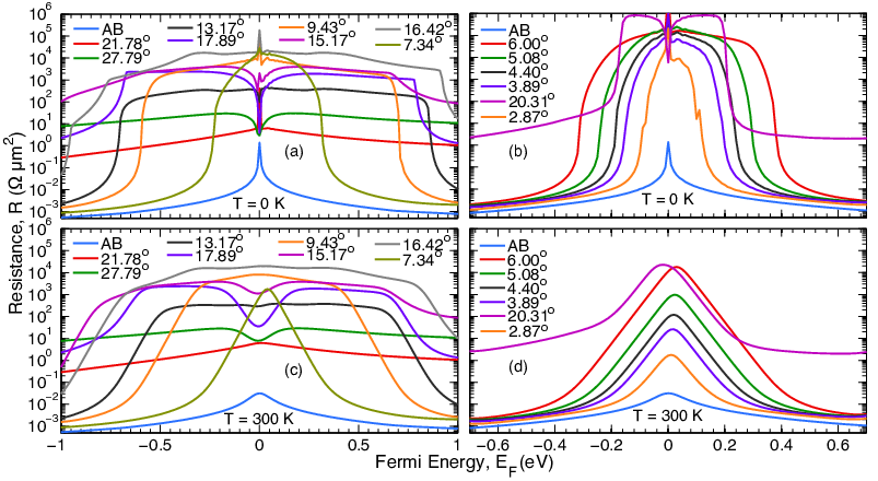
Figs. 2(a,b) show the zero-temperature, interlayer resistance over a range of Fermi energies from eV around the charge neutrality point in Fig. 2(a) and from eV in Fig. 2(b) for a range of rotation angles from to . The lowest curve is the coherent resistance of the ideal AB stack with o. This resistance is the fundamental limiting ‘quantum resistance’ inversely proportional to the number of transverse modes available to carry the current at a given energy. This quantity has recently been calculated for other materials to determine the fundamental lower limit on the contact resistance.[33]
The magnitude of the coherent interlayer resistance increases several orders of magnitude as the layers become misaligned. The legends in Figs. 2(a,b) are ordered according to the size of the corresponding commensurate unit cell so that, among the rotated interfaces, gives the smallest unit cell and gives the largest unit cell. For angles , the magnitude of the resistance increases with the size of the unit cell. This is the same trend found for the coherent, interlayer resistance of bilayer graphene discussed in Ref. [29]. The resistances for angles , fall off rapidly as the energy moves away from the charge neutrality point, so that at larger energies, this trend fails for the smaller rotation angles.
All of the angles shown except fall along the line of minimum unit-cell size shown in Fig. 2 of Ref. [23]. A one to two degree change in the rotation angle can change the commensurate unit cell size by over 3 orders of magnitude. Thus, it is interesting to consider two very close angles with a large difference in cell size. Two such angles are in Fig. 2(a) and in Fig. 2(b). These two angles differ by , yet the rotation gives the smallest unit cell with a lattice constant of Å, and the rotation gives the second largest unit cell with a lattice constant of Å. Near the charge neutrality point, the resistance of the structure is the highest of all of the structures. This follows the trend of increasing resistance with unit cell size. At energies eV away from the charge neutrality point, the resistance rapidly falls 4 to 5 orders of magnitude and approaches the resistance of the structure. This can be understood by considering the extended zone scheme of the reciprocal lattice. At this energy, the Fermi surfaces around the K points that coincide in the extended zone scheme of the structure just begin to touch.

We refer to the magnitude of the K points of the structure in the extended zone scheme as . They are illustrated in Fig. 3. They lie in the second Brillouin zones and their magnitude is where is the magnitude of the point in the first Brillouin zone, , and Å. At a rotation angle of , these points are misaligned by , and their centers are misaligned in -space by Å-1. The radius of the Fermi circle in the plane of ideal AB graphite at eV is . Thus, at eV in the structure, the Fermi surfaces begin to touch around the points. In the extended zone scheme, at low energies, in the structure, conduction takes place at points with a magnitude of . At eV, conduction begins at the points with a magnitude of . Since the matrix element coupling the states decays exponentially with the magnitude of , there is a sudden decrease in resistance when a channel opens at a much smaller -point in the extended zone.[28]
As the magnitude of the energy increases, new channels open around -points in the extended zone. When these points are closer to , the resistance suddenly drops and approaches a new value dominated by the transmission through the smaller points. For example, at eV, the structure begins to conduct around the points and its resistance falls several orders of magnitude to that of the structure. When the resistance falls to the same order of magnitude as that of the ideal AB structure, it indicates that the transmission is taking place around the -points of the first Brillouin zone. At higher energies, this is the dominant transport channel for all of the low-angle structures as can be seen in Fig. 2(b).
When a new channel opens up in the extended zone scheme, it will generally appear in the reduced zone of the commensurate primitive cell as a sudden movement of the transmission in -space. This results from the fact that new points in the extended zone do not, in general, map onto the points of the reduced Brillouin zone. For the structure, the transmission in the reduced Brillouin zone shifts from the point to the point at eV.
The coherent interlayer resistances at K are shown in Figs. 2(c,d). They are obtained by convolving the transmission with the room temperature thermal broadening function in Eq. (1) which removes the sharpest features from Fig. 2(a,b). At room temperature, the interlayer resistances for angles exponentially decay with energy torwards the ideal unrotated value.
The room temperature resistance values for all structures are plotted in Fig. 4 at a Fermi energy of 0.26 eV as considered in Refs. [28, 29] for rotated bilayer graphene. The values are also listed in Table 1. The trend of exponentially increasing resistance with unit-cell size is clear for rotation angles . An abrupt, three order of magnitude discontinuity in the trend occurs between and for the low rotation angles. In these structures, transmission is taking place around the -points of the first Brillouin zone.
There is also the one outlying point from the structure. While its unit-cell size is huge, and it is not a small angle, its resistance is far off of the initial trend. It has the same resistance as the smallest structure. That is because, at an energy of 0.26 eV, its transmission is taking place around the same points in the extended zone as that of the structure.
The vast number of huge commensurate primitive cells a small rotation angle away from much smaller primitive cells, as shown in Fig. 2 of Ref. [23], will not follow the exponential trend of resistance versus cell size at any energy a few hundred meV away from the charge neutrality point. Instead, their finite Fermi surfaces will overlap at some much reduced point in the extended zone, and those -points, corresponding to a much smaller cell size, will control the conductance.
In conclusion, the
quantum-resistance of ideal AB graphene
is on the order of .
For small misorientation angles,
the coherent interlayer resistance
exponentially decreases towards the ideal, unrotated
AB value at higher energies.
For intermediate angles of minimal cell sizes,
the coherent interlayer resistance
exponentially increases with cell size.
For intermediate angles with very large cell sizes,
the resistance will correspond to a much smaller
cell size of a nearby angle for any finite Fermi energy
of a few hundred meV.
Acknowledgement: This work was supported in part by FAME,
one of six centers of STARnet, a Semiconductor Research Corporation
program sponsored by MARCO and DARPA.
| Rotation Angle | Lattice Constant | No of Atoms | |
|---|---|---|---|
| AB | 2.46 | 2 | |
| 21.78 | 6.51 | 28 | 3.28 |
| 27.79 | 8.87 | 52 | 27.7 |
| 13.17 | 10.72 | 76 | 363 |
| 17.89 | 13.69 | 124 | 1860 |
| 9.43 | 14.96 | 148 | 4080 |
| 15.17 | 16.13 | 172 | 3720 |
| 16.42 | 17.22 | 196 | 16400 |
| 7.34 | 19.21 | 244 | 0.90 |
| 6.00 | 23.46 | 364 | 5.55 |
| 5.08 | 27.71 | 508 | 0.24 |
| 4.40 | 31.97 | 676 | |
| 3.89 | 36.23 | 868 | |
| 20.31 | 36.23 | 868 | 7.11 |
| 2.87 | 49.01 | 1588 |

References
- [1] L. Britnell, R. V. Gorbachev, R. Jalil, B. D. Belle, F. Schedin, A. Mishchenko, T. Georgiou, M. I. Katsnelson, L. Eaves, S. V. Morozov, N. M. R. Peres, J. Leist, A. K. Geim, K. S. Novoselov, and L. A. Ponomarenko, Science 335, 947 (2012).
- [2] H. Yang, J. Heo, S. Park, H. J. Song, D. H. Seo, K.-E. Byun, P. Kim, I. Yoo, H.-J. Chung, and K. Kim, Science 336, 1140 (2012).
- [3] S. Chuang, R. Kapadia, H. Fang, T. C. Chang, W.-C. Yen, Y.-L. Chueh, and A. Javey, App. Phys. Lett. 102 (2013), 10.1063/1.4809815.
- [4] T. Georgiou, R. Jalil, B. D. Belle, L. Britnell, R. V. Gorbachev, S. V. Morozov, Y.-J. Kim, A. Gholinia, S. J. Haigh, O. Makarovsky, L. Eaves, L. A. Ponomarenko, A. K. Geim, K. S. Novoselov, and A. Mishcheno, Nature Nanotechnology 8, 100 (2012).
- [5] W. J. Yu, Z. Li, H. Zhou, Y. Chen, Y. Wang, Y. Huang, and X. Duan, Nat. Mat. 12, 246 (2013).
- [6] W. Mehr, J. Dabrowski, J. Christoph Scheytt, G. Lippert, Y.-H. Xie, M. C. Lemme, M. Ostling, and G. Lupina, IEEE Elect. Dev. Lett. 33, 691 (2012).
- [7] D. Jena, Proc. IEEE 101, 1585 (2013).
- [8] A. K. Geim and I. V. Grigorieva, Nature 499, 419 (2013).
- [9] M. J. W. Rodwell, M. Le, and B. Brar, Proc. IEEE 96, 271 (2008).
- [10] G. J. Morgan and C. Uher, Phil. Mag. B 44, 427 (1981).
- [11] D. Z. Tsang and M. S. Dresselhaus, Carbon 14, 43 (1976).
- [12] S. Ono, J. Phys. Soc. Jap. 40, 498 (1976).
- [13] A. H. Castro Neto, F. Guinea, N. M. R. Peres, K. S. Novoselov, and A. K. Geim, Rev. Mod. Phys. 81, 109 (2009).
- [14] W. Primak and L. H. Fuchs, Phys. Rev. 95, 22 (1954).
- [15] T. Tsuzuku, Carbon 21, 415 (1983).
- [16] K. Matsubara, K. Sugihara, and T. Tsuzuku, Phys. Rev. B 41, 969 (1990).
- [17] G. Venugopal, G. S. Kim, and S.-J. Kim, Jap. J. Appl. Phys. 50, 06GE06 (2011).
- [18] B. Lopes dos Santos J. M., R. Peres N. M., and H. Castro Neto A., Phys. Rev. Lett. 99, 256802 (2007).
- [19] X. Wu, X. Li, Z. Song, C. Berger, and W. A. de Heer, Phys. Rev. Lett. 98, 136801 (2007).
- [20] S. Latil, V. Meunier, and L. Henrard, Phys. Rev. B 76, 201402 (2007).
- [21] J. Hass, F. Varchon, J. Millán-Otoya, M. Sprinkle, N. Sharma, W. de Heer, C. Berger, P. First, L. Magaud, and E. Conrad, Phys. Rev. Lett. 100 (2008).
- [22] S. Shallcross, S. Sharma, and O. A. Pankratov, Phys. Rev. Lett. 101, 056803 (2008).
- [23] S. Shallcross, S. Sharma, E. Kandelaki, and A. Pankratov O., Phys. Rev. B 81, 165105 (2010).
- [24] G. Trambly de Laissardiere, D. Mayou, and L. Magaud, Nano Letters 10, 804 (2010).
- [25] A. Luican, G. Li, A. Reina, J. Kong, R. R. Nair, K. S. Novoselov, A. K. Geim, and E. Y. Andrei, Phys. Rev. Lett. 106, 126802 (2011).
- [26] J. M. B. Lopes dos Santos, N. M. R. Peres, and A. H. Castro Neto, Phys. Rev. B 86, 155449 (2012).
- [27] S. Shallcross, S. Sharma, and O. Pankratov, Phys. Rev. B 87, 245403 (2013).
- [28] R. Bistritzer and H. MacDonald A., Phys. Rev. B 81, 245412 (2010).
- [29] V. Perebeinos, J. Tersoff, and P. Avouris, Phys. Rev. Lett. 109, 236604 (2012).
- [30] Y. Kim, H. Yun, S.-G. Nam, M. Son, D. S. Lee, D. C. Kim, S. Seo, H. C. Choi, H.-J. Lee, S. W. Lee, and J. S. Kim, Phys. Rev. Lett. 110, 096602 (2013).
- [31] S. Ahsan, K. M. Masum Habib, M. R. Neupane, and R. K. Lake, J. Appl. Phys. 114, 183711 (2013).
- [32] See supplementary material for more detailed calculation methods.
- [33] J. Maassen, C. Jeong, A. Baraskar, M. Rodwell, and M. Lundstrom, App. Phys. Lett. 102, 111605 (2013).