Voltage Controlled Switching Phenomenon in Disordered Superconductors
Abstract
Superconductor-to-Insulator transition (SIT) is a phenomenon occurring for highly disordered superconductors and is suitable for a superconducting switch development. SIT has been demonstrated to be induced by different external parameters such as temperature, magnetic field, electric field, etc. However, electric field induced SIT (ESIT), which has been experimentally demonstrated for some specific materials, holds the promise of any practical device development. Here, we demonstrate, from theoretical considerations, the occurrence of ESIT. We also propose a general switching device architecture using ESIT and study some of its universal behavior, such as the effect of sample size, disorder strength and temperature on the switching action. This work provides a general framework for development of such a device.
Introduction
Superconducting switch has been in development for the past 60
years. The first attempt was the development of cryotron, which was
a magnetic field driven switching of a superconductor [1].
There has also been several attempts to generate FET architecture
using superconductors[2],[3].
The discovery of superconductor to insulator transition (SIT) for
disordered superconductors [4] opened up doors for a new
switching mechanism. SIT was particularly attractive, because unlike
the metal to superconductor transition, SIT provided a much larger
change of the current with one phase being superconductor and hence
zero resistance and the other being insulator and hence infinite
resistance (ideally). However, such transition was driven by either
magnetic field, or disorder modification or temperature change
[5], making such phenomenon unsuitable for application
in integrated circuits.
Quite recently there have been a few demonstrations of electric
field driven SIT. Though these works hold the promise of leading to
a further development of superconducting electronics, all of them
are demonstrated for very specific materials and no microscopic
analysis of such process was given
[3],[6],[7] .
In this work, we first demonstrate strong fluctuation of
superconducting pair amplitude with electron density (number of
electrons per lattice site), for a strongly disordered
superconductor system. We start with negative U Hubbard model, Eq.
1, describing a disordered superconductor. From this
model, we then show the strong dependence of the superconducting
pair amplitude, an internal parameter governing the
superconductivity of a sample, on the average density of electron
per lattice site. We then demonstrate that such strong fluctuations
can lead to SIT, through phase correlation calculations. Based on
this phenomenon, we then propose a general architecture of a
superconducting switch, a device, capable of switching from
superconducting state, with effectively zero resistance, to an
insulating state, with resistance of the order of
[5]. Even though there are few realizations of such a
device, most of them requires a large change of electron density to
bring about a change of phase, as is evident from the high values of
voltage needed to switch such a system. The device we are proposing
is driven by a quantum phenomenon
[8],[9],[10], where small changes of
electron density can lead to a change of phase, hence requiring a
small amount of voltage change, compared to current
experimental devices.
Finally, we study some universal properties , namely the effect of
sample size, disorder strength and temperature
on the behaviour of the device.
Model and Methods
We model the disordered superconductor using a negative-U Hubbard Hamiltonian on a square lattice. The Hamiltonian is given by
| (1) |
Here () is the creation
(annihilation) operator for an electron at site with a spin
, represents the hopping energy, is a site
dependent random potential with uniform distribution from to
, is the chemical potential and is the strength of the
attractive interaction between two electrons of opposite spins at
the same site.
In this model, represents the kinetic energy of the electrons
and all other parameters are scaled with . represents the
same site interaction between electrons of the opposite spins and
represent the cooper attraction giving rise to superconductivity.
The partition function for this model is given by,
| (2) | |||||
where is the hermitian conjugate and is the inverse temperature in the unit where Boltzmann constant is unity. We introduce the Hubbard-Stratonovic transformation with a local Hubbard-Stratonovic field given by . is the order parameter with being the pair amplitude and being the phase. Under this transformation, the partition function becomes,
| (3) | |||||
where with
which would
be calculated by self-consistency.
Bogoliubov-de Genne approximation: The Hubbard-Stratonovic field () can be obtained by applying Bogoliubov-de Genne approximation (BdG). In BdG approximation the partition function is evaluated at the saddle point. Under this approximation, we obtain an effective Hamiltonian given by
| (4) | |||||
The Hamiltonian has to follow two self-consistent relations, namely, and . is diagonalized by a Bogoliubov transformation . The local Bogoliubov amplitudes are obtained by the following equation,
| (5) |
Here represents the single particle contribution of and are the eigenvalues [11]. The self consistent relations in terms of the Bogoliubov amplitudes are
| (6) |
| (7) |
Starting from some initial guess values, we self-consistently obtain the values of and for each lattice site . We define the spatial average of as given by
| (8) |
The average electron density per lattice site is defined as
| (9) |
We can change the average electron density () in the sample by
controlling the chemical potential (). The BdG approximation
gives the saddle point solution for the . However, it has
completely missed the fluctuations of phase , due to
its mean-field nature.
Fluctuations around the Saddle point: To incorporate phase fluctuations we go beyond BdG and introduce a newly developed method [12],[13] which allows us to calculate classical phase fluctuations while ignoring time dependence of the order parameter (quantum fluctuations). Under this approximation the partition function becomes,
| (10) |
In terms of eigenvalues of equation(5), the partition function reads,
| (11) |
For obtaining the fluctuations around the saddle point, we relax the self-consistent constraint on and calculate the value of for all possible values of through Eq. (5) (for a particular disorder realization).Using the values of thus obtained, we can evaluate the values of and the expectation value of any observable given by
| (12) |
We have checked that for the temperature range we are interested in,
the values of are practically the same as
its value evaluated in BdG approximation. However, has a
strong dependence on temperature. Therefore we replace
in Eq. 12 by its BdG value and hence we only need to
integrate over . The integration over is
performed using Monte Carlo method [12],[13]. The
energy eigenvalues
can be ignored while calculating Eq. 12.
Using the partition function , it has been shown that for weak
disorder, the system shows small fluctuations of pair-amplitudes
while preserving long range phase correlation. Strong disorder on
the other hand, leads to strong fluctuations of the pair-amplitudes
because of the formation of superconducting islands and also
destroys the long range phase correlation. This phenomenon has also
been recently experimentally observed [14]
[15].
Electric field driven SIT (ESIT)
At strong disorder, is strongly dependent on the value of , as is demonstrated in Figure 1. This strong fluctuation of with is due to rapid change in local density of states around the small window near the fermi-surface [8]. The key feature of this fluctuation is that, the fluctuation only takes place when the sizes of the superconducting islands become comparable to the superconducting coherence length, . Our main motivation is to induce an SIT by controlling the size and distribution of the islands, which can be achieved by tuning .
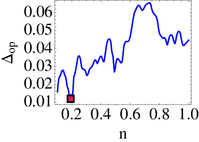
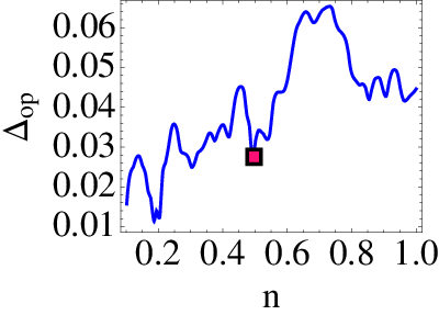
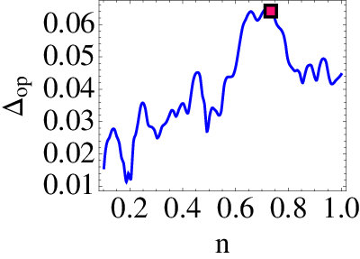
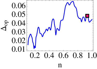


The tuning of the electron density can be achieved by applying suitable electric fields. For a first order calculation, we assume a classical dependence. The electric field inside the two electrodes separated by a distance is , where is the applied voltage. Therefore charge density on the surface is where is the dielectric constant. Because of the condition of equilibrium in a metal the additional charge density on the surface of the superconductor is exactly equal to . To convert this charge density into the electron density per lattice we divide it by where is electronic charge and is the lattice constant on the superconducting plane. Therefore, we obtain the dependence of electron density on applied electric field as
| (13) |
where and is the electron
density per lattice site for .
The electric field is applied perpendicular to the plane of the
superconductor. It is assumed that the disorder superconductor is
only on the plane whereas in the direction it is metal.
This assumption holds for a thin layer of disordered superconductor
such that the thickness in the axis is much less than the
coherence length and hence it can be treated as a metal along that
axis. For a more realistic situation, the functional dependence of
will change, but the basic principal of modification of
electronic distribution via electric field remains the same.
Thus we can obtain a SIT driven by applied potential across the sample. Since this transition is driven by small changes of the values of , hence small values of applied potential can lead to a switching of the sample from superconducting state to an insulating state.
Device Construction Using ESIT
The strong dependence of on the electron density and
control of the electron density using an electric field opens up the
possibility of developing a voltage control device which switches
between insulator and superconductor states. Because of this strong
dependence, a small change of electron density ()
can drive the system from insulator to superconductor and vice
versa. This, in turn,
implies that a small voltage change (from Eq. (13)) is required to drive this switching operation.
To demonstrate the switching action, we calculate the edge-to-edge
phase correlation for a given sample as a function of electron
density. The edge-to-edge pase correlation is defined as [16]
| (14) |
Here and correspond to site indices at the two opposite edges of the lattice. We have used a lattice on the xy plane with the edges from to and to . For calculating the edge-to-edge phase correlation, we sum over all the lattice sites on the edge. This is because in an actual device, phase correlation between all the lattice sites on the edge will contribute. We have assumed a periodic boundary condition along the x-axis and an open boundary condition along the y-axis. We assume the current flowing in the y direction and hence we need to measure the phase correlation along the y-axis.
A non-zero value of edge-to-edge phase correlation implies a
superconducting state and effectively zero resistance current flow
[16] . Lack of such correlation even in the presence of
superconducting islands is typical signature of insulating states
associated with SIT
[15],[17],[18],[19]. Such
states have much higher resistance () compared to
the superconducting states and a sample in such a state
can effectively work like an open circuit. Figure demonstrates the switching phenomenon.


We can now use this switching phenomenon to construct a device which
can act as a voltage controlled electronic switch. The basic
architecture is shown in the Figure . The switching takes place
on the
plane whereas the control field acts in the direction.

Effect of Sample Size, Disorder Strength and Temperature on Switching
The operational efficiency of the device depends on the strength of
the disorder (), the sample size of the device, compared to the
coherence length (), and the operating temperature ().
Effect of Sample Size: Figure demonstrates the effect of
sample size on the fluctuation of the superconducting pair
amplitude. If , then the fluctuations of
with would increase and the stability of the
switch would be affected. On the other hand, for , the fluctuation reduces and the switching
property can be suppressed. The switching property arises because of
the strong fluctuation of with . As shown in Fig.
1, for a particular value of , we have large and closely spaced
superconducting islands, corresponding to large value of
, whereas, for another value of we have large
non-superconducting regions, corresponding to smaller values of
. This is true for a system size comparable to the
coherence length. However, for , even though in
regions of size comparable to , we have strong pair
amplitude fluctuation with , on the scale of the system size,
change of electron density merely rearranges the position of the
superconducting islands and hence the global properties like
and edge-to-edge phase correlation doesn’t show a
significant dependence on , leading to the suppression of the
switching property. Thus for efficient operation, suitable sample
size must be selected, depending on the coherence length of
the material used.


Effect of Disorder Strength: In the weak disorder regime, the
effect of electron density on the value of is
insignificant. However, stronger the disorder, greater is this
effect, as is demonstrated in Fig. 5. This happens because of rapid
change of superconducting landscape of a sample with a small change
of electron density in strong disorder regime. A strong change of
local density of states depending on the value of leads to this
changing landscape as is described in Ref. [8].
Sample size and disorder strength give us two handles to control the
change of electron density required for performing the switching
action. By changing the sample size and the disorder strength, we
can change the fluctuation of with and hence we
can control the change of density required for the system to switch
from insulating state to superconducting state and vice versa. For
example, if it is needed to decrease the change of required for
the switching, one can increase the disorder strength or reduce the
sample size or both.


Effect of Temperature: Within the range we are working,
finite temperature will have insignificant effect on the
superconducting landscape and hence . However, the
edge-to-edge phase correlation will have a strong dependence on the
temperature. This in turn, will effect certain properties of the
switching action, such as the switching point (the voltage or the
electron density about which the system undergoes a transition from
insulator to superconductor), switching gap (the difference of the
value of across the switching point),etc. As can be seen in
Figure , with change of temperature, the difference between the
switching states changes. This, in turn, can effect the stability of
the switch. Figure demonstrates the effect of temperature on the
switching gap. However, the switching point (), i.e.
, remains independent of temperature,
where and are the values of at
superconducting and insulating states respectively. The invariance
of the switching point with temperature can be attributed to the
fact that for low temperatures, the landscape of pair amplitude
across the sample, remains almost invariant. On the other hand, the
change of the switching gap arises because of the decrease of the
phase correlation in the superconducting state with
an increase of temperature.

Discussions and Conclusions
The strong dependence of pair amplitude on the average electron
density have thus enabled us to postulate a device, capable of
switching between insulator and superconductor states, driven by
very small change of electron density. The requirement of small
change of electron density in turn implies that a small voltage
change is required to drive the switching mechanism. In the example
we have shown (Fig. ), the total change of the electron density
is along the x-axis. However, the change of electron density
across the transition point is as low as .
We have used the following values of material properties for Eq.
13- , and
, where is the
free space permittivity. For these parameters, we need a voltage
change of (density change ) for switching. However, by
controlling the disorder and sample size, we can modify the
switching voltage
appropriately.
A typical coherence length is of the order of . Therefore a
typical system size can be be of the order of . However,
one can change the size of a typical device by using materials
having different coherence lengths. For example, by using aluminium,
one can construct devices with size of the order of tens of microns,
where as by using materials such as alloys of and , one can
construct devices of the order of tens of nanometers. Also the
architecture provided is a very basic FET structure. But in the a
realistic situation, the architecture might be completely different
and material dependent.
Individual characteristics of a device, such as the change in
electron density for the transition, the electron density about
which the transition occurs, the switching gap, etc, are strongly
sample dependent. Different samples with different disorder
realization will have different switching points, switching gaps,
etc. However, the phenomenon of the strong dependence of
on , and ESIT is independent of the disorder
landscape. Averaging over different disorder realization will erase
the fluctuations but since a single sample will contain a particular
disorder realization, disorder averaging is less informative in this
context.
The architecture of this device gives us an distinct advantage over
the previous attempts, since it can provide a possible adaptation of
superconducting switches in integrated circuits. Also, the
theoretical treatment allows us to claim in a generalized manner
that such a switch can be developed, though the exact material,
optimal for application, can only be determined experimentally. With
proper system, such a design can potentially usher in
superconducting electronics, which can improve
the efficiency and capability of large computational systems.
Acknowledgements
We would like to thank Prof. Shudhansu Shekhar Mondal for valuable discussions.
References
- [1] D. A. Buck, The Cryotron-A Superconductive Computer Component, Proc. of IRE, 44, 482 (1956).
- [2] T. Nishino et. al., 0.1 Gate-Length Superconducting FET. IEEE Electron Device Lett., 10, 61-63, (1989).
- [3] J. H. Schon et al. A Superconducting Field-Effect Switch, Science 288, 656 (2000).
- [4] Y. Liu et. al., Scaling of the Insulator-to-Superconductor Transition in Ultrathin Amorphous Bi Films, Phys. Rev. Lett. 67, 2068, (1991).
- [5] A. M. Goldman and N. Markovic, Superconductor-Insulator Transitions in the Two-Dimensional Limit, Phys. Today 51, 39 (1998).
- [6] M. Gabay and J. M. Triscone, Superconductors: Terahertz superconducting switch, Nature Photonics 5, 447 (2011).
- [7] Kevin A. Parendo et. al., Electrostatic Tuning of the Superconductor-Insulator Transition in Two Dimensions, Phys. Rev. Lett. 94, 197004 (2005).
- [8] Sanjib Ghosh and Sudhansu S. Mandal, Shell effect in strongly disordered superconductors. arXiv:1307.0609, (2013)
- [9] A. M. Garcia-Garcia et al., BCS superconductivity in metallic nanograins: Finite-size corrections, low-energy excitations, and robustness of shell effects, Phys. Rev. B. 83, 014510 (2011).
- [10] S. Bose et. al., Observation of shell effects in superconducting nanoparticles of Sn, Nature Materials 9, 550 (2010).
- [11] Amit Ghosal, Mohit Randeria and Nandini Trivedi, Role of Spatial Amplitude Fluctuations in Highly Disordered s-Wave Superconductors. Phys. Rev. Lett., 81, 3940 (1998).
- [12] Yonatan Dubi, Yigal Meir and Yshai Avishai, Nature of the superconductorinsulator transition in disordered superconductors. Nature, 449, 876 (2007).
- [13] M. Mayr, G. Alvarez, C. Sen, and E. Dagotto, Phase fluctuations in strongly coupled d-wave superconductors, Phys. Rev. Lett. 94, 217001 (2005)
- [14] A. Kamlapure et. al., Emergence of nanoscale inhomogeneity in the superconducting state of a homogeneously disordered conventional superconductor, Scientific Reports 3, 2979 (2013)
- [15] B. Sacepe et. al., Disorder-Induced Inhomogeneities of the Superconducting State Close to the Superconductor-Insulator Transition, Phys. Rev. Lett. 101, 157006 (2008).
- [16] A. Erez and Y. Meir, Thermal phase transition in two-dimensional disordered superconductors, Europhys. Lett. 91, 47003 (2010).
- [17] D. Kowal, and Z. Ovadyahu, Disorder induced granularity in an amorphous superconductor, Solid State Commun., 90, 783-786 (1994).
- [18] R. W. Crane et. al. Survival of superconducting correlations across the two-dimensional superconductor-insulator transition: A finite-frequency study, Phys. Rev. B 75, 184530 (2007).
- [19] B. Sacepe et. al., Localization of preformed Cooper pairs in disordered superconductors, Nature Physics 7, 239-244 (2011).