Electro-Thermo-Chemical Computational Models for 3D Heterogeneous Semiconductor Device Simulation
Abstract.
In this article we propose and numerically implement a mathematical model for the simulation of three-dimensional semiconductor devices characterized by an heterogeneous material structure. The model consists of a system of nonlinearly coupled time-dependent diffusion-reaction partial differential equations with convection terms describing the principal electrical, thermal and chemical phenomena that determine the macroscopic electrical response of the device under the action of externally applied electrical and thermal forces. The system is supplied with suitable initial, boundary and interface conditions that account for the interaction occurring among the various regions of the device with the surrounding environment. Temporal semi-discretization of the problem is carried out with the Backward Euler Method while a fixed-point iteration of Gummel type is used for system decoupling. Numerical approximation of the linearized subproblems is carried out using an exponentially fitted stabilized Finite Element Method on unstructured tetrahedral grids. Several computational experiments are included to validate the physical accuracy of the proposed computational algorithm in the study of realistic device structures.
Keywords: Semiconductors; electronic and memory devices; nonlinear reaction-diffusion system with convection; interface conditions; numerical simulation; finite element method.
1. Introduction
The continuous scaling of semiconductor devices has pushed contemporary research and most prominent technologies towards the use of innovative materials where new physical phenomena occur. In this context, an important class of applications is represented by resistive memories. In the case of Phase Change Memories (PCM) the resistive state is determined by a controlled switch of a calchogenide between the crystalline and the amorphous phase [34]. Here recent studies have clearly demonstrated the onset of a significant mass transport among different components of the calchogenide alloys. In other devices, the Resistive Random Access Memories (ReRAM), the low and high resistance state [32] is realized by using and controlling non-equilibrium thermo-chemical reactions Moreover, in most of these new applications, the active material of the device (where transport, diffusion and reaction processes occur) is no longer homogeneous but often displays a markedly heterogeneous structure, as in the case of advanced logic devices. Finally, during the specific device application, the main physical material properties are not constant but also evolve in time due to the extreme working conditions (i.e., high electric and/or thermal fields).
A multidisciplinary approach is clearly fundamental to describe the basic functionality of heterogeneous devices in the correct physical framework. As a matter of fact, even if the exploration of materials properties can be effectively understood and theoretically simulated with the help of “ab-initio ”calculations [27], the electrical response and the time scale of operation of such devices still need to be addressed with the advanced mathematical methods traditionally employed in electronic, mechanical and thermal simulation. The novel challenge introduced by the technological application considered in the present article is that theoretical elements of semiconductor device physics, chemical, thermal and mechanical properties, must be included within a unified model setting in order to allow self-consistent calculations that account for the mutual interplay among the various phenomena occuring in the same device. This strong requirement reflects into a similar constraint in the numerical treatment of the problem because standard simulation suites are no longer usable but they need to be integrated and in some cases completely developed from scratch.
For these reasons, in this article we have developed a general mathematical and numerical framework in which the different physical contributions to the simulation can be effectively incorporated and mutually coupled to reach the desidered self-consistency and model accuracy.
The mathematical model consists of a system of nonlinearly coupled time-dependent diffusion-reaction partial differential equations (PDEs) with convection terms describing the principal electrical, thermal and chemical phenomena that determine the macroscopic electrical response of the device under the action of externally applied electrical and thermal forces (see [5, 13] and [14, 18, 19, 11]). The system is supplied with initial, boundary and interface conditions that account for the interaction occurring among the various regions of the device with the surrounding environment.
The numerical approximation of the problem is conducted in two distinct steps. In the first step, temporal semi-discretization is carried out with the Backward Euler Method using a non-uniform time stepping. In the second step, a fixed-point iteration of Gummel type is adopted for system decoupling [22]. This leads to solving a sequence of linearized advection-diffusion-reaction equations that are numerically treated using an exponentially fitted stabilized Finite Element Method (FEM) [16, 35, 12] on unstructured tetrahedral partition of the computational domain. The FEM is chosen in the present discrete formulation of our model because it can properly address the complexity of the three-dimensional geometry (3D), avoiding any requirement of symmetry often used as a simplification and offering at the same time the adequate flexibility to implement all the mathematical and physical models needed in these emerging applications.
An outline of the article is as follows. Sect. 2 illustrates the fundamental conservation laws that express mass and energy balance of a system of charged species in a material medium under the combined effect of electrical, thermal and chemical forces. Sect. 3 is devoted to the description of the multi-domain geometrical structure of the 3D semiconductor device object of the present study while Sect. 4 describes how to adapt the general thermo-electrochemical theory of Sect. 2 to the mathematical modeling of the class of devices of Sect. 3. The resulting formulation deals with the case of a single negatively charged species (electrons, ) and consists of a nonlinearly coupled system of advection-diffusion-reaction PDEs that have to be solved in a heterogeneous domain supplied by a set of initial and boundary conditions. Sect. 5 is, instead, devoted to illustrate the three main computational steps which allow to translate the differential problem of Sect. 4 into the successive solution of linear algebraic systems providing the approximate solution of the problem. Sect. 6 is devoted to the validation of the physical accuracy of the computational model through the simulation of 3D device structures under realistic working conditions. Sect. 7 draws the main conclusions reached in the present article and addresses possible future research developments. Appendix A contains a list of all the symbols introduced in the article, specifying for each symbol the associated physical meaning and units.
2. Modeling of Thermo-Electrochemical Phenomena
In this section we introduce the fundamental conservation laws that express mass and energy balance of a charged multi-species system moving in a material medium under the combined effect of electrical, thermal and chemical forces. For a complete treatment of electrochemical phenomena and of the mathematical foundations of non-equilibrium thermodynamics, we refer to [5] and to, e.g., [13]. For the mathematical analysis of general reaction-diffusion thermo-chemically coupled systems, we refer, e.g., to [14, 18, 19, 11] and to the bibliography cited therein.
Let be the total number of chemicals flowing in the medium under the action of electrical, chemical and thermal forces. We denote by , , the number density of the -th chemical at the spatial position and time , and by its ionic valence (equal to zero if the species is electrically neutral). We set . We also introduce the dependent variables and representing the temperature of the medium and the electric field at the spatial position and time , respectively.
2.1. Conservation laws
The basic form of the mathematical model considered in this article is constituted by the following coupled system of PDEs in conservation form:
| (1a) | ||||
| (1b) | ||||
| (1c) | ||||
Eqns. (1a) are the continuity equations for the chemicals , , where is the current density associated with each chemical and is the corresponding net production rate accounting for recombination and generation phenomena in the medium.
Eq. (1b) is the energy balance equation in the system, where and are the mass density and the specific heat of the medium, respectively, is the energy flux density in the medium while is the net heat production rate.
Eq. (1c) is the Poisson equation expressing Gauss’ law in differential form, where is the electron charge, is the dielectric permittivity of the medium and is a given function of position that accounts for the possible presence of fixed ionized dopant impurities. Assuming the quasi-static approximation in Maxwell’s equations (see [29]), the electric field can be expressed as
| (1d) |
where is the electrostatic potential at each spatial position in the medium and time .
2.2. Constitutive relations
In this section, we provide the mathematical characterization of the fluxes and and of the other model parameters in system (1). To this purpose, we follow the classical references [24, 13] and, for more recent applications, [8, 11], and assume that both current density and energy flux density can be expressed as the sum of two contributions, namely, an electrochemical flux and a thermal flux, so that:
| (2a) | ||||
| (2b) | ||||
2.2.1. Electrical fluxes
Let denote the electrical conductivity of species defined as
| (3) |
where is the electrical mobility of the -th species.
The electrochemical flux associated with is [5]:
| (4a) | ||||
| (4b) | ||||
where is the electrochemical potential of the -th species given by the sum of the electrical potential and of the chemical potential
| (5) |
and being the chemical energy of the -th species and Faraday’s constant, respectively. In a homogeneous material (), is constant so that the electrochemical potential is just a constant shift of the electric potential. In a non-homogeneous material (), the chemical energy is defined as
| (6) |
where is the ideal gas constant and is a reference concentration, so that the electrochemical potential is [5]
| (7) |
where is Boltzmann’s constant.
Let us now consider the thermal current density . We have [8]:
| (8a) | ||||
| (8b) | ||||
where is the thermal potential, being the thermopower coefficient of the material.
Gathering together the above definitions of the various flux and potential contributions, we can write a generalized Ohm’s law for the current density associated with the -th chemical:
| (9a) | ||||
| (9b) | ||||
| (9c) | ||||
where is the thermo-electrochemical potential of the -th chemical and is the thermo-electrochemical field experienced by the -th chemical.
Remark 2.1 (The generalized Drift-Diffusion model).
Replacing (3) into (9) we obtain the following equivalent form of the current density associated with the -th chemical:
| (10a) | ||||
| (10b) | ||||
| (10c) | ||||
where is the generalized diffusion coefficient of the -th chemical, related to the electrical mobility through the generalized Einstein relation (10c) and is the generalized electric field experienced by the chemical . Thus, Eq. (10a) represents the generalized Drift-Diffusion (DD) model for ionic charge transport in a non-homogeneous and non-isothermal material. If the material is in isothermal conditions and electrons and holes are considered for transport, relation (10a) degenerates into the classical DD model [22]. In this case, two chemicals are flowing in the material (), namely, negatively charged electrons () and positively charged holes ().
2.2.2. Thermal flux
Let denote the thermal conductivity of the material. Then, classical Fourier law states that heat thermal flow in the material is expressed by the following relation
| (11) |
Heat is also transported in the direction of the total current flow in the material according to the following relation [13]
| (12) |
where:
| (13a) | ||||
| (13b) | ||||
are the total thermo-electrochemical potential and current density, respectively. Gathering together the above definitions of the various flux and potential contributions, we can write the thermo-electrochemical heat flux in a concise advection-diffusion form
| (14) |
2.3. Model coefficients, sources and sinks
To complete the description of the thermo-electrochemical model we need specify the mathematical form of the physical parameters and coefficients. For sake of simplicity, we assume henceforth that the net production rates and are identically equal to zero. These assumptions are equivalent to state that sources and sinks in the material bulk accounting for mutual interactions among the chemicals are neglected in our description. Concerning the other model parameters, we assume from now on that the electrical mobilities , the thermopower , the dielectric permittivity , the thermal conductivity , the mass density and the specific heat and are constant positive quantities whose numerical values are specified in Sect. 6.
Example 2.1 (The case of silicon devices).
A significant example of the application of the thermo-electrochemical model illustrated in this section is provided by the study of silicon devices traditionally employed in the semiconductor technology for microelectronics applications. The corresponding version of system (1) including Joule heat dissipation but not thermo-electric power effects, is usually referred to as Energy-Transport (ET) model (see [22]). The extension of the ET to cover also thermo-electric mechanisms (Peltier and Thomson effects) can be found in [9].
3. Geometry and structure of the device
In this section we address the geometrical description of the semiconductor device object of the present work. Fig. 1(a) shows a perspective view of a typical 3D template devices for electronics applications. More complex device configurations will be investigated in Sect. 6. The device is characterized by an intrinsically material heterogeneous structure composed of an active region (yellow layer) sandwiched between two inactive regions (red and grey blocks). These latter regions accomplish several important functions: 1) they provide electrical and thermal connection with the external environment, allowing to apply a voltage and thermal drop across the device; 2) one of them supplies the intermediate active region with the appropriate thermo-electrochemical driving energy; and 3) the other one collects the thermo-electrochemical current flux produced by the active region and transfers it to the external circuit connected in series to the device for further use.


In view of the mathematical modeling of the problem, we consider in the present article the slightly simplified schematic geometrical representation illustrated, with a two-dimensional (2D) cut view, in Fig. 1(b). The device region is an open bounded domain consisting of the union of three subdomains: the two inactive regions, (top) and (bottom), and the intermediate active layer, . The external boundary of the device, , is made of the union of three open disjoint surfaces, , and , on which an outward unit normal vector is defined.
The top and bottom surfaces, and , are the electrical and thermal contacts where external voltage and thermal sources are applied. The lateral surface of the device, , is the material interface between the device and the external environment whose temperature is denoted by . The portion of belonging to the boundary of the active region is denoted henceforth as .
The intermediate subdomain is separated from the top inactive region by the interface surface on which we define the normal unit vectors and , outwardly directed on each surface with respect to and . In a similar manner, on the bottom interface surface separating from the inactive region we define the normal unit vectors and , outwardly directed on each surface with respect to and . Clearly, on and on .
4. Mathematical Model of a 3D Semiconductor Device
In this section we use the basic theory developed in Sect. 2 to construct the thermo-electrochemical mathematical model of the 3D heterogeneous semiconductor device introduced in Sect. 3. From now on, we denote by the time interval in which we study the dynamical behaviour of the device and we assume that:
- (A1):
-
the two inactive regions and are metals or degenerate semiconductors;
- (A2):
-
charge transport in the device active region is only due to electrons that are injected by tunneling from one of the inactive regions into the active layer.
Based on (A2), we limit ourselves to considering the case and set , being the electron number density in the device. Based on (A1), we also set:
| (15) |
where and are the constant values of the electron concentration in the two metallic domains. Relations (15) express the fact that the two metal regions and are homogeneous conductors, so that electrical conductivity is uniform (equal to and , respectively) and electric current transport is governed by the ideal Ohm’s law. Finally, we assume that the chemical energies of the bottom and top metal regions are constant values equal to and , respectively, the thermopower coefficient is a piecewise constant function equal to and in the bottom and metal regions, respectively, and to in the active region, the electron electrical mobility is a positive constant in the active region and the mass density and specific heat are piecewise constant positive functions equal to , , and , , , respectively.
Replacing (10) and (14) into (1) and using (15), we end up with the following system of PDEs in conservation form to describe the thermo-electrochemical processes occurring in a 3D heterogeneous semiconductor device:
| (16a) | ||||
| (16b) | ||||
| (16c) | ||||
The chosen ordering of the equations in system (16) reflects the structure of the solution map that is used to iteratively solve the problem as illustrated in Sect. 5.
Eq. (16a) represents a generalized Poisson equation in the whole device, because it coincides with the differential Gauss’ law (1c) in the active region while in the two metal regions it takes the form and meaning of an electro-thermal Ohm’s law, having defined in a piecewise manner over the device domain the electro-thermal flux as:
| and the space charge density as: | ||||
Eq. (16b) is the electron continuity equation in the active region, the electron current density being defined as
| (18) |
Eq. (16c) is the heat flow equation in the whole device structure, the total heat flux being defined as
| (19a) | ||||
| where the thermo-electrochemical potential and density flux are defined in a piecewise manner over the device domain as: | ||||
| (19b) | ||||
| and: | ||||
| (19c) | ||||
To complete the mathematical model of thermo-electrochemical transport in a semiconductor device, we need specify suitable initial and boundary conditions.
Concerning the initial conditions, we set:
| (20a) | ||||
| (20b) | ||||
where and are given positive functions.
Concerning the boundary conditions, for all we set:
| (21a) | ||||
| (21b) | ||||
| (21c) | ||||
| for the generalized Poisson equation, and: | ||||
| (21d) | ||||
| (21e) | ||||
| (21f) | ||||
| for the electron continuity equation, and: | ||||
| (21g) | ||||
| (21h) | ||||
| (21i) | ||||
for the generalized heat equation.
Let us address the mathematical and physical interpretation of the above boundary conditions.
Relations (21a)- (21b) are non-homogeneous Dirichlet boundary conditions for the electric potential expressing the physical fact that the electric contacts are equipotential surfaces equal to the externally applied voltage sources and .
Relations (21c)- (21f) are homogeneous Neumann conditions expressing the physical fact that charge transport in the device is self-contained, i.e., current lines start and close between the two bottom and top surfaces.
Relation (21d) is a non-homogeneous Neumann condition for the electron flux, being the (positive) electron current density injected by tunneling from the bottom metal region into the active layer across the separating surface .
Relation (21e) is a Robin boundary condition expressing the net electron current flux flowing between the active region and the top metal region across the separating interface surface . The mathematical form of this boundary condition is analogous to that used to describe current flux balance at a Schottky interface between a metal and a semiconductor accounting for thermoionic emission (from the metal) and drift-diffusion injection (from the semiconductor) [31]. According to this interpretation, and are the values of drift velocity and electron concentration at thermodynamical equilibrium conditions while is the unknown value of electron number density on the interface side of the active layer.
Relations (21g)- (21h) are non-homogeneous Dirichlet boundary conditions for device temperature expressing the physical fact that the electric contacts are also equi-thermal surfaces equal to the externally applied positive thermal sources and .
Relation (21i) is a Robin boundary condition expressing the net heat flux exchange between the device and the surrounding environment, being a non-negative heat transfer coefficient.
Remark 4.1 (The nature of the model).
It is interesting to notice that the coupled set of equations (16)- (17) supplemented by the initial conditions (20) and boundary conditions (21) constitute an incompletely parabolic system of PDEs because of the need of satisfying the elliptic constraint (16a) at each time level. This issue makes the treatment of the problem quite difficult, both in analytical and numerical terms.
5. Computational Techniques
In this section we describe the various steps that transform the PDE model (16)- (21) into the successive solution of linear systems of algebraic equations of large size that represent the discrete counterpart of the problem.
5.1. Time semi-discretization
We divide the time interval into a finite number of time slabs of nonuniform width , with , in such a way that discrete time levels are denoted as , . The choice of a nonuniform discretization of the time variable is made in order to properly track the wide dynamical range of the temporal scales of the thermo-electrochemical phenomena occuring in the device under investigation which may vary between nanoseconds to milliseconds up to even seconds. In the present computer implementation, the sequence of values of is user-defined and for time advancing the Backward Euler (BEM) method is adopted because of its unconditional stability. An alternative approach based on the use of higher-order methods coupled with adaptive strategies for automatic time-step selection (see, e.g., [4, 23, 1]) will be considered in a future extension of the computational scheme proposed in the present article.
5.2. Solution map
Throughout the remainder of the article, given a function
we set
for every . We also denote by ,
and the characteristic functions of the sets ,
and , respectively,
such that if
and if
, .
The functional iteration illustrated
below is used to linearize the thermo-electrochemical model
upon previous time
semidiscretization with the BEM:
given , , execute the following
solution steps:
A) set ;
B) for until convergence, solve:
| (22a) | ||||
| with: | ||||
| and set ; | ||||
| (22b) | ||||
| with: | ||||
| and set ; | ||||
| (22c) | ||||
| with: | ||||
| and set . | ||||
C) Let denote the solution triple. Should the sequence be converging to a fixed point , then set:
| (22d) |
and proceed to the next time level.

The solution map (22) can be regarded as the extension of the Gummel decoupled iteration widely employed in contemporary semiconductor device simulation (see [29]) and thoroughly analyzed in [22]. The study of existence (and possible uniqueness) of a fixed point of (22) and of the convergence of the solution map as a function of model physical parameters goes beyond the scope of the present article and will be the object of a future publication.
The three steps A), B) and C) of the functional iteration (22) are schematically represented in the flow-chart of Fig. 2 where the symbol GPE in the first block indicates the linear Generalized Poisson Equation (22a), while ECE and HFE denote the linear Electron Continuity Equation (22b) and the linear Heat Flow Equation (22c), respectively. The criterion adopted to monitor the convergence of the solution map (22) is to stop the algorithm at the first value of the iteration counter such that
where is a prescribed tolerance, denotes the vector of nodal degrees of freedom of the finite element approximation and
is the -norm of a vector . In the numerical experiments we have set .
5.3. Numerical approximation
In this section we carry out the numerical approximation of each linear boundary value problem in the Gummel iterative process (22) using the Galerkin Finite Element (FE) method. To this purpose, we introduce a partition of the domain into regularly shaped [10] tetrahedral elements of average size , denoting the discretization parameter. On the triangulation , we define the finite dimensional space
| (23) |
of piecewise affine functions that are continuous over the computational domain. The dimension of is denoted henceforth by and coincides with the number of vertices of .
The standard Galerkin FE method consists of finding the approximation of the weak solution of each problem in (22) (see [26]) and gives rise to the solution of a linear system of algebraic equations
| (24) |
where is the stiffness matrix, is the vector of nodal values , , while is the load vector. The formulation may suffer of unwanted instabilities in the case where reaction and/or convection terms dominate over the diffusion term. Such instabilities typically show up under the form of spurious oscillations in the computed numerical solution which, in extreme cases, may even give rise to negative values of . This latter event is physically not acceptable, should represent a number density or a temperature.
The simple-minded remedy to overcome these problems is to reduce the mesh size , at the price, however, of a considerable increase of the computational effort which may become overwhelming in 3D simulations. An alternative approach consists of introducing into the FE formulation suitable stabilization terms as discussed in [7, 15, 6, 26]. These stabilized FE methods prevent (or strongly limit) the onset of spurious oscillations preserving at the same time the optimal convergence properties of the plain FE approximation but are not able, in general, to ensure the computed solution to be non-negative.
Since in our application (and more in general, in thermo-electrochemical models) the property of of being non-negative is critical because of the physical meaning of the unknown (temperature, number density), in this article we adopt the exponentially fitted or edge-averaged finite element scheme thoroughly discussed and analyzed in [2, 3, 16] (in two spatial dimensions) and in [35, 25, 12] (also in three spatial dimensions). The method is a multi-dimensional extension of the classical Scharfetter-Gummel difference scheme [28] and gives rise to the linear algebraic system
| (25) |
where is the stiffness matrix associated with the exponentially fitted discretization, is the corresponding solution vector while the right-hand side is the same as in (24). According to Lemma 5.1 of [35], it can be shown that is a M-matrix [33] under suitable conditions on the shape regularity of the triangulation . This property implies the following important result which expresses the well-posedness and monotonicity of the discrete problem.
6. Simulations and Results
The model and the computational algorithm described in Sect. 4 and Sect. 5 have been implemented in a numerical code written in C++ 98 and compiled with gcc 4.5.2 in shared libraries on 64-bit architectures and run on multiple cores blades. The code has then been applied to the simulation of several 3D structures with a cubic or cylindrical shape of which some examples are shown in Fig. 3.


Fig. 3 visualizes typical meshes built with tetrahedra used in the discretization procedure. Cubic structures are geometrically discretized using a general Delaunay mesh generator because the most important surfaces are axis aligned. In the case of cylindrical structures a Delaunay mesher able to build a boundary conformal mesh employing surface-adapted, anisotropic, mesh layers has been used in order to properly account for the influence of the interfaces on the boundary conditions [30]. The resulting meshes are constituted by a number of elements varying from 90000 to 450000 depending on the simulated structure. All the reported simulation results show the computed solutions at steady-state conditions. In the case of -size structures the final time needed for steady-state to be reached is of the order of , while in the case of cylindrical -size structures the final time needed for steady-state to be reached is of the order of . The typical computational time for the presented cases varies between a minimum of 30 minutes to a couple of hours maximum. In all reported simulation data and results, physical model parameters and variables are expressed in the units of the International System according to the list of Sect. A, except for the length scale which is expressed in for graphical convenience.
6.1. Comparison with analytical solutions
This section is devoted to the comparison of the computed 3D numerical solution with the 1D analytical solution obtained for simple cases. For this purpose, as reference structure we have used a cubic device characterized by different values of the thickness and imposed homogeneous Neumann boundary conditions on , and . Firstly, we have tested Eq. (1a) with and a constant given electric field of strength equal to considering three different chemical species with charge and ( being the electron charge). For each species, the initial condition is set constant in all and equal to . A linear variation of temperature from to is imposed to the structure. Geometrical thicknesses are and . Fig. 4 reports the results of the numerical simulation (1D cuts along the axis in the center of the plane) compared with the analytical solution: symbols are for the numerical and lines for the analytical results. No difference has been found between our implementation and the exact stationary solution.

Secondly, we have considered Eq. (16c) with an electric field directed along the axis, , where is the unit vector of the axis. If an uniform concentration of electrons () is imposed in all we can neglect the contribution coming from the diffusion term so that (19) reduces to
| (27) |
where is the electron mobility. In this condition Eq. (16c) can be solved analytically. The considered thicknesses of the cubic structure are and . Robin boundary conditions have been enforced and with and and , while homogeneous Neumann conditions are enforced on . Initial condition for temperature is set constant to in all . For convenience of the reader, Tab. 1 reports the values of the parameters used during the comparison.
| Parameter | value |
|---|---|
Fig. 5 shows a 1D cut along the axis in the center of the plane of the 3D numerical solutions compared with the exact analytical ones in the stationary case (symbols are for numerical and lines for analytical values). To measure the relative weight of thermal diffusion with respect to thermal convection it is useful to introduce the local Pèclet number
| (28) |
denoting the average mesh size used in the computations, equal to . In the three considered cases () the values of are , and , respectively, this indicating that in the first case the thermal flow is dominated by convection while in the other two cases diffusion is the principal transport mechanism of heat in the device. It is important to notice that in the case , the use of the exponentially fitted FEM prevents the onset of spurious oscillations without introducing any extra amount artificial thermal diffusion. In all the simulated cases a very good agreement between numerical and analytical solution is found.

6.2. Heterogeneous material
As discussed in Sect. 1, heterogeneous materials are widely used in a new emerging application like PCM devices. In this section we report the results of the numerical simulations in a heterogeneous medium for the model of Sect.4. The test cases (denoted a, b and c) consist in cubic structures ( and ) where the transport region, , is divided along the axis into three zones with thickness of 3, 4 and 3, respectively. Tab. 2 reports the different parameters used in each of the regions separated by a comma. For sake of clarity, Tab. 3 shows the boundary conditions applied to the simulation domain for Eq. (16a) to (16c), the symbols D, N and R denoting Dirichlet, Neumann and Robin types, respectively. We note that thermal and electrical gradients are directed towards . Initial conditions are set constant in for all transport equations to the value of for electrons and for temperature.
| Parameter | a | b | c |
|---|---|---|---|
| Equation | boundary | type | value |
|---|---|---|---|
| Eq. (16a) | D | ||
| Eq. (16a) | D | ||
| Eq. (16a) | N | Homogeneous | |
| Eq.(16b) | R | ; | |
| Eq. (16b) | R | ; | |
| Eq. (16b) | R | ; | |
| Eq. (16c) | R | ; | |
| Eq. (16c) | R | ; | |
| Eq. (16c) | R | ; |
Fig. 6 shows the electron concentration obtained by the numerical simulations in the three different cases: because of symmetry reasons we have reported the solutions on the axis and the coordinates of the simulation plane on the plane.


For case a) electrons are forced towards the bottom interface place at because thermal power is high enough to force electrons moving against the electric field. Case b) is exactly the opposite of case a): electrons are moving along the electric field but against the thermal gradient towards : the different values of the peaks for cases a) and b) depend of the different values of the electron mobility chosen in the device regions. More complex to interpret are the results showed for case c) in which a charge accumulation is found in the center (along the axis) of the active regions: this is due to the chosen low electron mobility in this region and the opposite effects of thermal and electrical gradients.
1D cuts along the axis in the center of the simulation plane are shown in Fig. 7. In particular, Fig. 7(a) shows electron concentration as in Fig. 6 clarifying the accumulation of the electrons at the top and bottom interface or at the center of the cube. Fig. 7(b) shows the temperature profiles: the different thermal conductivity chosen for the various region of the devices is resulting in different thermal velocities justifying the difference in the profiles.


6.3. Cylindrical shape
Sect. 1 has already pointed how geometries can be very complex in the new devices due to the miniaturization technological process. A typical example is the case of a cylindrical shape that can simulate the gate all around or three gate devices such those employed in the SONOS memories [17], or in the FinFET CMOS [20] and [21] . The numerical implementation of the model of Sect. 4 has been here applied to study the cylinder of Fig. 3(b) with and . In Tabs. 4 and 5 we have reported the parameters and the boundary conditions used in the simulations. We note that thermal and electrostatic gradients are in the same directions towards the center of the cylinder in the last two boundary condition for Eq. (16a), while in the first boundary condition they are in the opposite direction. Moreover the boundary conditions result in an injection of electrons from the surface inside . Initial conditions are set constant in in the transport equations with for electrons and for temperature.
| Parameter | value |
|---|---|
| Equation | boundary | type | values |
|---|---|---|---|
| Eq. (16a) | D | ||
| Eq. (16a) | D | ||
| Eq. (16a) | N | Homogeneous | |
| Eq. (16b) | R | ; | |
| Eq. (16b) | R | ; | |
| Eq. (16b) | R | ; | |
| Eq. (16c) | R | ; | |
| Eq. (16c) | R | ; | |
| Eq. (16c) | R | ; |
Fig. 8 shows the numerical solution of Eq. (16a) for the three different applied bias on : as expected, the potential is a continous function overall the device and the gradient direction is swapping between the first and the last two values.
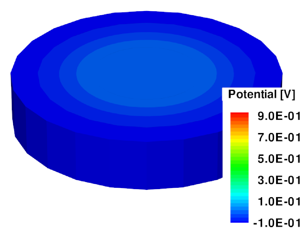
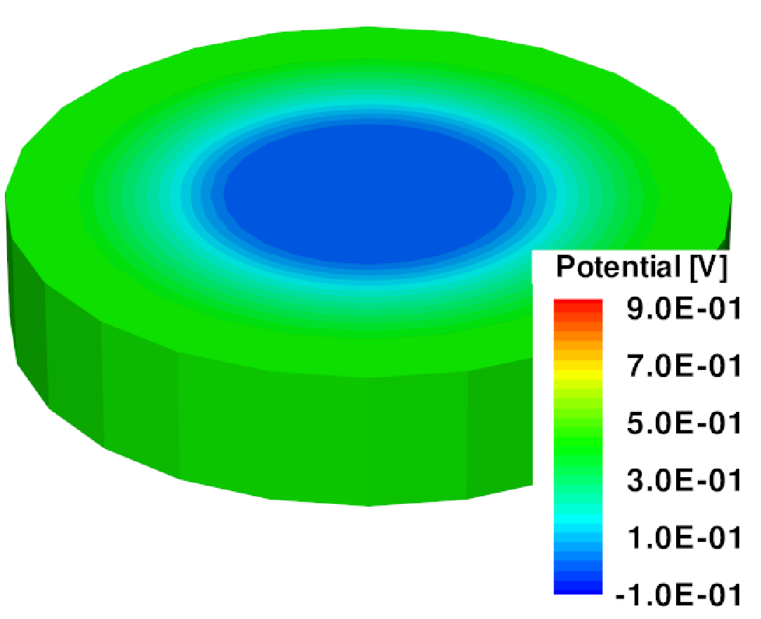
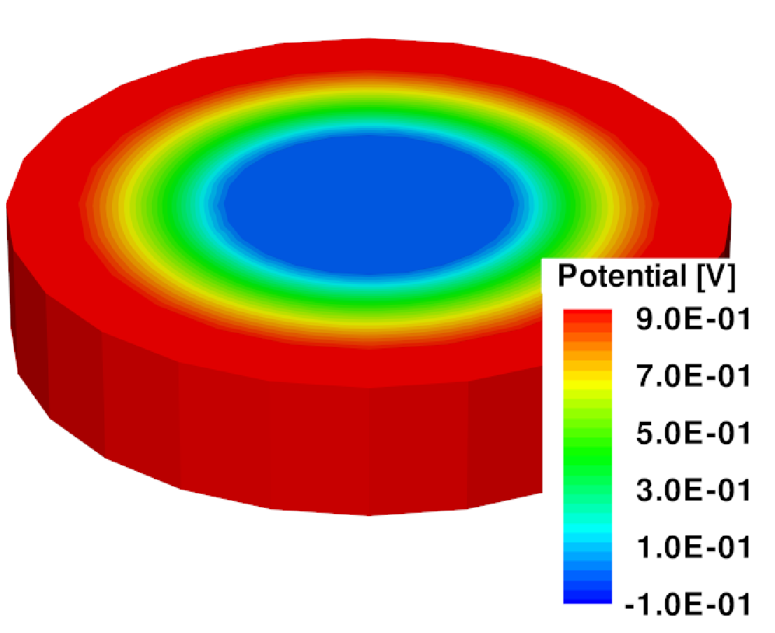
Fig. 9 shows 1D cuts at and of electron concentration (cf. Eq. (16b)) for three different applied bias on . Even if electrons are injected in from , in the case with on electric and thermal gradients are pushing electrons back towards . This results in very low diffused profiles. In the latter two cases, on the contrary, the electric field is high enough to dominate over the thermal gradient and hence electrons can diffuse towards .

7. Conclusions and Future Perspectives
In the present article we have provided a unified mathematical framework capable of describing the complex and interplaying electro-thermo-chemical processes that occur in modern new emerging technologies in semiconductor device industry.
The general conservation law format of the model building block equations allowed us to successfully adapt to the presently investigated application: 1) the functional iteration tools usually employed in standard electronic transport device simulation programs, and 2) the Finite Element Exponentially Fitted discretization technique that, in conjunction with a suitable tetrahedral geometrical partition of the computational domain, is characterized by enjoying a discrete maximum principle for chemical number densities and temperatures.
Model and computational algorithms have been thoroughly validated by the numerical study of several realistic device geometries for which, in some simple albeit significant cases, exact analytical solutions were available. Results have always been characterized by a very good mathematical accuracy and close agreement with physically expected solution behaviour, clearly demonstrating the potentiality of model and numerical tools in providing close insights and fine prediction for outperforming devices of the next node generation.
Future steps in our research programme in this new emerging area include:
- (1)
further validation of the proposed computational model through calibration against measured data;
- (2)
inclusion of mechanical stress analysis in the model;
- (3)
analysis of the existence of a fixed point and convergence of the functional iteration (22);
- (4)
analysis of well-posedness of each differential subproblem in the iterative map (22);
- (5)
Acknowledgements
The authors gratefully acknowledge Giovanni Novielli and Silvia Sorbello (MSc degree students in Mathematical Engineering at Politecnico di Milano) for their contribution in the development of the simulation program and of the numerical results.
References
- [1] U.M. Ascher and L.R. Petzold, Computer methods for ordinary differential equations and differential-algebraic equations, SIAM, 1998.
- [2] R.E. Bank, J.F. Burgler, W. Fichtner, and R.K. Smith, Some upwinding techniques for finite element approximations of convection-diffusion equations, Numer. Math. 58 (1990), 185–202.
- [3] R.E. Bank, W.M. Coughran Jr., and L.C. Cowsar, The finite volume Scharfetter–Gummel method for steady convection–diffusion equations, Comput. Visual. Sci. 1(3) (1998), 123–136.
- [4] R.E. Bank, Jr. W.M. Coughran, W. Fichtner, E.H. Grosse, D.J. Rose, and R.K. Smith, Transient simulation of silicon devices and circuits, IEEE Trans. on CAD CAD-4 (1985), no. 2, 436–451.
- [5] A.J. Bard and L.R. Faulkner, Electrochemical methods: Fundamentals and applications (2nd ed.), Wiley, 2001.
- [6] F. Brezzi, L.P. Franca, T.J.R. Hughes, and A. Russo, , Comput. Methods Appl. Mech.Engrg. 145 (1997), 329–339.
- [7] A.N. Brooks and T.J.R. Hughes, Streamline upwind Petrov-Galerkin formulations for convection dominated flows with particular emphasis on the incompressible Navier-Stokes equations, Comput. Meths. Appl. Mech. and Engr. 32 (1982), 199–259.
- [8] M.V. Cheremisin, Peltier-effect-induced correction to ohmic resistance, Journal of Experimental and Theoretical Physics 92 (2001), no. 2, 357–360 (English).
- [9] P. Ciampolini, A. Pierantoni, A. Liuzzo, and G. Baccarani, 3d simulation of silicon devices: physical models and numerical algorithm, Process and Device Modeling for Microelectronics (G. Baccarani, ed.), Elsevier North-Holland, Amsterdam, 1993, pp. 53–107.
- [10] P.G. Ciarlet, The Finite Element Method for Elliptic Problems, North Holland, Amsterdam, 1978.
- [11] L. Consiglieri, On the posedness of thermoelectrochemical coupled systems, The European Physical Journal Plus 128 (2013), no. 5, 1–16 (English).
- [12] C. de Falco, Quantum–corrected drift–diffusion models and numerical simulation of nanoscale semiconductor devices, Ph.D. thesis, Università degli Studi di Milano, 2006.
- [13] S.E. de Groot and P. Mazur, Non-equilibrium thermodynamics, Dover, 1984.
- [14] P. Degond, S. Génieys, and A. Juengel, A system of parabolic equations in nonequilibrium thermodynamics including thermal and electrical effects, J. Math. Pures Appl. 76 (1997), 991–1015.
- [15] L.P. Franca, S.L. Frey, and T.J.R. Hughes, Stabilized finite element methods: I. application to the advective–diffusive model, Comput. Methods Appl. Mech.Engrg. 95 (1992), 253–276.
- [16] E. Gatti, S. Micheletti, and R. Sacco, A new Galerkin framework for the drift-diffusion equation in semiconductors, East-West J. Numer. Math. 6(2) (1998), 101–135.
- [17] C. Gerardi, E. Tripiciano, G. Cina, S. Lombardo, C. Garozzo, D. Corso, G. Betro, C. Pace, and F. Crupi, Multiple gate nvm cells with improved fowler- nordheim tunneling program and erase performances, Solid State Electronics 54 (2010), no. 11, 1319–1325.
- [18] A. Glitzky and R. Huenlich, Global estimates and asymptotics for electro-reaction-diffusion systems in heterostructures, Appl. Anal. 66 (1997), 205–226.
- [19] A. Glitzky and A. Mielke, A gradient structure for systems coupling reaction-diffusion effects in bulk and interfaces, Z. Angew. Math. Phys. 64 (2013), 29–52.
- [20] D. Hisamoto, W.-C. Lee, J. Kedzierski, E. Anderson, H. Takeuchi, K. Asano, T.J. King, J. Bokor, and C. Hu, A folded-channel mosfet for deep-sub-tenth micron era, Proc of IEEE International Electron Devices Meeting Technical Digest (1998), 1032–1034.
- [21] X. Huang, W.-C. Lee, C. Kuo, D. Hisamoto, J. Kedzierski, E. Anderson, H. Takeuchi, Y.-K.Choi, K. Asano, V.Subramanian, T.J. King, J.Bokor, and C.Hu, Sub 50-nm finfet; pmos, Proc of IEEE International Electron Devices Meeting Technical Digest (1999), 67–70.
- [22] J.W. Jerome, Analysis of charge transport, Springer-Verlag, Berlin Heidelberg, 1996.
- [23] J.D. Lambert, Numerical methods for ordinary differential systems: The initial value problem, Wiley, 1991.
- [24] L.D. Landau, E.M. Lifshitz, and L.P. Pitaevskii, Electrodynamics of continuous media, Course of Theoretical Physics, vol. 8 (2nd Ed.), Butterworth-Heinemann, 1984.
- [25] R.D. Lazarov and L.T. Zikatanov, An exponential fitting scheme for general convection–diffusion equations on tetrahedral meshes, Comput. Appl. Math., (Obchysljuval’na ta prykladna matematyka, Kiev) 1(92) (2005), 60–69.
- [26] A. Quarteroni and A. Valli, Numerical approximation of partial differential equations, Springer-Verlag, New York, Berlin, 1994.
- [27] R.Car and M.Parrinello, Unified approach for molecular dynamics and density-functional theory, Physical Review Letters 55 (1985), no. 22, 2471–2474.
- [28] D. L. Scharfetter and H. K. Gummel, Large sygnal analysis of a silicon read diode oscillator, IEEE Trans. Electron Devices (1969), 64–77.
- [29] S. Selberherr, Analysis and simulation of semiconductor devices, Springer-Verlag, Wien-New York, 1984.
- [30] Synopysis, User manual version f-2011.09, 2011.
- [31] S.M. Sze and K.K. Ng, Physics of semiconductor devices (3rd ed.), Wiley, 2006.
- [32] I. Valov, R. Waser, J.R. Jamenson, and M.N. Kozicki, Electrochemical metallization memories-fundamentals, applications, prospects, Nanotechnology 22 (2011), 1–22.
- [33] R.S. Varga, Matrix iterative analysis, Englewood Cliffs, New Jersey, 1962.
- [34] H.-S. Wong, S.Raoux, S. Kim, J.Liang, J.P. Reinfenberg, B.Rajendran, M.Asheghi, and K.E. Goodson, Phase change memory, Proceeding of the IEEE 98 (2010), no. 12, 2201–2227.
- [35] J. Xu and L. Zikatanov, A monotone finite element scheme for convection–diffusion equations, Math. Comp. 68(228) (1999), 1429–1446.
Appendix A List of symbols
Below, we provide a summary of all the variables, physical constants and parameters that have been introduced throughout the article, specifying for each symbol the meaning and units.
| Symbol | Meaning | Units |
|---|---|---|
| position vector | ||
| time variable | ||
| total number of chemicals | ||
| ionic valence | ||
| number density | ||
| temperature | ||
| electric potential | ||
| electric field | ||
| net production rate | ||
| current density | ||
| energy flux density | ||
| mass density | ||
| specific heat | ||
| net heat production rate | ||
| dielectric permittivity | ||
| net doping | ||
| electrochemical current flux | ||
| thermal current flux | ||
| electrochemical heat flux | ||
| thermal heat flux | ||
| electrical mobility | ||
| electrical conductivity | ||
| chemical potential | ||
| electrochemical potential | ||
| chemical energy | ||
| reference concentration | ||
| thermal potential | ||
| thermopower coefficient | ||
| thermo-electrochemical field | ||
| thermo-electrochemical potential | ||
| diffusion coefficient | ||
| generalized electric field | ||
| thermal conductivity | ||
| total thermo-electrochemical flux | ||
| total thermo-electrochemical potential |
| Symbol | Meaning | Units | Numerical Value |
|---|---|---|---|
| electron charge | |||
| Boltzmann constant | |||
| ideal gas constant | |||
| Faraday constant |