Generation of a fully valley-polarized current in bulk graphene
Abstract
The generation of a fully valley-polarized current (FVPC) in bulk graphene is a fundamental goal in valleytronics. To this end, we investigate valley-dependent transport through a strained graphene modulated by a finite magnetic superlattice. It is found that this device allows a coexistence of insulating transmission gap of one valley and metallic resonant band of the other. Accordingly, a substantial bulk FVPC appears in a wide range of edge orientation and temperature, which can be effectively tuned by structural parameters. A valley-resolved Hall configuration is designed to measure the valley polarization degree of the filtered current.
The low-energy electronic elementary excitations in bulk graphene originate from the out-plane - hybridization.[1] Their massless energy dispersion is well described by Dirac cones at the six corners of the Brillouin zone.[2] The six cones can be divided into two inequivalent groups labeled by the valley index and . Intervalley coupling or scattering requires a rather large change of the momentum and is thus suppressed in clean graphene samples. This independence suggests that the valley degree of freedom could be utilized as an information carrier.[3, 4, 5, 6, 7, 8]
How to generate a high-contrast valley population of charge carriers is a fundamental goal of graphene valleytronics. Several proposed valley filters require either a point contact with zigzag edges[3] or a breaking of the inversion symmetry.[4, 5] These factors may break the specific bulk elementary excitation that is essential for most of the excitement about graphene,[9, 10] such as Klein tunneling, nonzero minimum conductivities, and half-integer quantum Hall effect. Therefore, several schemes of valley filtering have been proposed based on bulk graphene, utilizing either valley-dependent trigonal band warping,[6] or pseudo magnetic fields induced by strain.[7] However, the generated valley polarization is shown to be low even at zero temperature.
In this Letter we present a scheme to achieve a fully valley-polarized current (FVPC) in bulk graphene. The proposed valley filter is a strained graphene under a periodic magnetic modulation [see Fig. 1(a)]. We show that, the combination between the periodic magnetic field and the strain can lead to a coexistence of insulating transmission gap of one valley and metallic resonant band of the other. Under this mechanism, the bulk FVPC survives in a wide range of edge orientation, temperature, and structural parameters. We also discuss how to measure the valley polarization degree of the output current.

Suppose that the magnetic superlattice consists of ferromagnetic metal (FM) strips. Each FM strip () has a size along the direction, a magnetization , a distance to the nearest strip(s) [see Fig. 1(b)], and is close enough to the graphene plane. The induced magnetic field can be approximately described[7] by the vector potential . Here is the Heaviside step function, , the size of a unit cell, and . The uniaxial tensile strain is homogeneous in the whole filtering region, i.e., and . It leads to changes in the nearest-neighbor hopping amplitudes, and can be described by pseudo magnetic vector potentials.[10, 11] When the edge orientation (the -axis) has an angle with respect to the armchair direction [see Fig. 1(c)], the pseudo vector potential reads with . Here and is the total length of the filtering region.
In the low-energy continuum approximation, the Hamiltonian for a given valley is[9] where for the valley and , is the Fermi velocity, is the pseudospin Pauli matrices, and is the momentum operator. For brevity, hereafter we express all quantities in dimensionless form by means of a characteristic length nm and energy unit meV. We assume that the sample width so that edge details are not important.[12] For an electron with energy and incident angle , the envelope function in each region () of the building block has the form
| (1) |
Here is the conserved transverse momentum, , with being a common gate voltage on all FM strips, , , , and .
The wave amplitudes and are determined from the continuity of the envelope function and the scattering boundary condition and . We write
| (2) |
where () is the transfer matrix for the superlattice unit cell . By means of the matrix and the condition and , one can express as[13]
| (3) |
From Eq. (3) we get and the matrix element , with , , and . Here we have used the identity . The transfer matrix for the finite superlattice is . From the recurrence relation and , we obtain the matrix elements of [14]
| (4) |
Here , , , and .
The total transfer matrix determines the valley-resolved transmission coefficient . The transmission probabilities read
| (5) |
where , , , , and .
Recent mobility measurements on graphene indicate that the electron-phonon scattering can be ignored in the temperature range of 10-100.[15] In this range, the ballistic valley-resolved conductance is given by the Landau-Büttiker formula[16]
| (6) |
where is the Fermi-Dirac distribution function at the temperature and the Fermi energy , and is the quantum conductance (2 accounts for the spin degeneracy). The zero-temperature conductance can be rewritten as , where is half of the number of the transverse modes and is the maximal channel conductance per valley.
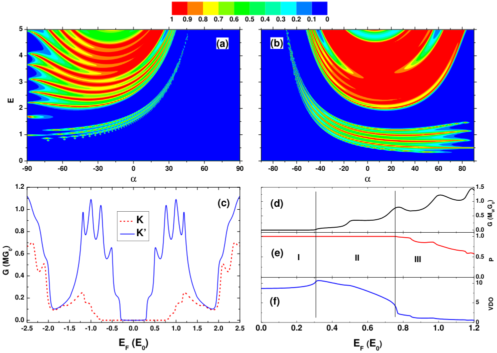
In Fig. 2 we present the results for and . As the incident energy decreases, the transmission demonstrates obvious quasi transparent region and transmission gap [see Figs. 2(a) and 2(b)]. The transmission gap is divided into two parts by a resonant region of --fold splitting. These observations are typical features of a periodic structure, which come from the -th power terms in Eq. (4). As a result, the valley conductance displays obvious quasi ballistic region, resonant band (), and blocked region ( with ) in the Fermi energy windows , , and , respectively [see Fig. 2(c)]. For valley , the transmission is suppressed in a wider energy window and the conductance in the resonant band becomes smaller. This is because the total vector potential () acting on electrons is distinct in amplitude from its counterpart for electrons.
A direct consequence is that, when the Fermi energy falls into the window II marked in panels (d)-(f) of Fig. 2, the current from valley is almost totally blocked while the current from valley possesses the order of the maximal channel conductance. Such coexistence of the blocked region of one valley and resonant band of the other renders the outgoing current a bulk FVPC (contributed mainly by electrons). This is clearly reflected from the valley difference in orders-of-magnitude (VDO) of the outgoing currents, [see Fig. 2(f)]. In the window I [], although the valley polarization is as good as in the window II, the rather small conductance makes it impossible for either detection or applications. The generation mechanism is rather similar to that for the nearly 100% spin-polarized current in half-metals,[17] i.e., the coexistence of metallic nature and insulating nature for electrons with opposite spin orientations. Very recently, a FVPC has also been predicted in ferromagnetic silicene junctions.[18] Due to the intrinsic gap, a much simpler single-junction design is sufficient for the FVPC generation. When the unit cells’ sizes differ, the and ranges for resonant tunneling become smaller meanwhile the transmission is strongly suppressed.[19] This leads to smaller conductance in narrower resonant bands for both valleys, hence a smaller FVPC in an operation window at higher energy.
The dependence of the total conductance and valley polarization on the edge orientation is shown in Fig. 3. It is evident that the total conductance (polarization) is a periodic function of with a period (). In addition, VDO is antisymmetric (symmetric) with respect to the angle (). These observations result from the dependence of on the edge orientation[20] and the symmetry . Thus it is sufficient to consider only the angle interval . Within this range a larger leads to a narrower window of Fermi energy where the VDO is high [Fig. 3(a)]. Actually, for (the zigzag direction), the valley polarization completely disappears because [Figs. 3(c) and 3(d)]. A remarkable FVPC (high VDO with substantial ) can be obtained under and relatively high Fermi energies. It can be also achieved under and relatively low Fermi energies. Under such values, electrons in valley feel alternate modulations of total vector potential along the direction, which lead to an almost transparent transmission [dashed curves in Fig. 3(d)]. In the following we will focus only on the armchair edge ().

We now consider the effect of temperature, which is shown in Fig. 4. The rich oscillations in the conductance spectrum at zero temperature are gradually smeared out as the temperature increases. Generally, the valley currents decrease (increase) with the temperature in the resonant bands (blocked regions). This leads to increasing total current in window I and decreasing VDO in window II (see Fig. 4(a) (b)). As a result, both windows I and II become smaller and disappear with the increase of temperature (see Fig. 4(c)). These behaviors can be understood from Eq. (6). Valley currents at a finite temperature are determined by the zero-temperature valley currents in an estimated energy range . In this range a dramatic variation of with energy results in an obvious temperature effect. Nevertheless, we can still obtain a bulk FVPC in a wide range of Fermi energy at a low temperature [see Fig. 4(c)].
The tunability of a FVPC source is desirable for valleytronic applications. In Fig. 5, we examine the influences of structural parameters such as the number of superlattice units and the strain strength . For simplicity, the ratio and are fixed at . When increases from to , the total conductance is lowered slightly and more conductance peaks appear [see Eq. (4)]. As the optimal VDO increases greatly, we can obtain bulk FVPC at higher temperatures in an almost unchanged energy window. However, the choice of should guarantee that the total length is smaller than the electron mean free path and valley coherent length. With the increasing of , bulk FVPC can appear in a wider Fermi energy window and the optimal VDO also increases, while the conductance decreases greatly. Thus the strain (and magnetization) strength should be chosen as moderate. All the results above are obtained under electron-hole symmetry. If this symmetry is broken by a common negative gate voltage on all FM strips, the conductance in the hole (electron) region increases (decreases) but the VDO decreases (increases). Both the conductance and VDO curves shift towards the hole region. As a result, the inclusion of a negative (positive) electric potential is helpful for obtaining bulk FVPC for electrons (holes) in lower energy and at higher temperature.
The injection of a valley-polarized current into a gapped graphene will lead to a finite Hall voltage.[4] This mechanism can be utilized to measure the valley polarization degree of the filtered current [see Fig. 1(b)]. Due to the effective valley dependent gaps[5] () changes slightly to () in the detection region. The voltage between the upper (lower) edge and the middle region () is proportional to ().[4] Thus and VDO can be respectively reflected by and , especially when the gap is small. A rather huge positive (negative) is an evidence for that we obtain a FVPC of valley ().
In summary, we have demonstrated that a strained graphene under the modulation of a finite magnetic superlattice can generate a bulk FVPC. The FVPC appears in a wide range of edge orientation angles and temperature. The underlying mechanism is the coexistence of the metallic resonant band and insulating transmission-blocked region of two valleys in a certain Fermi energy window. Such a mechanism implies that superlattices consisting of any valley filtering structures can be used to generate a FVPC. The FVPC can be effectively controlled by tuning the structural parameters, and may be used as a high-quality current source of bulk valleytronics. A valley-resolved Hall configuration is suggested to measure the valley polarization degree of the filtered current.
F.Z. acknowledges support from the NSFC Grant No. 11174252. Y.G. acknowledges support from the NSFC Grant No. 11174168 and the 973 Program Grant No. 2011CB606405.
References
- [1] P. Wallace, Phys. Rev. 71, 622 (1947).
- [2] G.W. Semenoff, Phys. Rev. Lett. 53, 2449 (1984).
- [3] A. Rycerz, J. Tworzyd, and C. W. J. Beenakker, Nature Phys. 3, 172 (2007).
- [4] D. Xiao, W. Yao, and Q. Niu, Phys. Rev. Lett. 99, 236809 (2007).
- [5] F. Zhai and K. Chang, Phys. Rev. B 85, 155415 (2012); D. Moldovan, M.R. Masir, L. Covaci, and F.M. Peeters, ibid. 86, 115431 (2012).
- [6] J.M. Pereira Jr., F.M. Peeters, R.N. Costa Filho, and G.A. Farias, J. Phys.: Condens. Matter 21, 045301 (2009).
- [7] F. Zhai, X.F. Zhao, K. Chang, and H.Q. Xu, Phys. Rev. B 82, 115442 (2010); A. Chaves, L. Covaci, Kh.Yu. Rakhimov, G.A. Farias, and F.M. Peeters, ibid. 82, 205430 (2010); T. Fujita, M.B.A. Jalil, and S.G. Tan, Appl. Phys. Lett. 97, 043508 (2010); F. Zhai and L. Yang, ibid. 98, 062101 (2011).
- [8] D. Gunlycke and C.T. White, Phys. Rev. Lett. 106, 136806 (2011); L. Jiang, G. Yu, W. Gao, Z. Liu, and Y. Zheng, Phys. Rev. B 86, 165433 (2012); J.N.B. Rodrigues, N.M.R. Peres, and J.M.B. Lopes dos Santos, ibid. 86, 214206 (2012).
- [9] C. W. J. Beenakker, Rev. Mod. Phys. 80, 1337 (2008).
- [10] A. H. Castro Neto, F. Guinea, N. M. R. Peres, K. S. Novoselov, and A. K. Geim, Rev. Mod. Phys. 81, 109 (2009).
- [11] V.M. Pereira and A.H.C. Neto, Phys. Rev. Lett. 103, 046801 (2009).
- [12] J. Tworzydło, B. Trauzettel, M. Titov, A. Rycerz, and C.W.J. Beenakker, Phys. Rev. Lett. 96, 246802 (2006).
- [13] M. Born and E. Wolf, Principles of Optics: Electromagnetic Theory of Propagation, Interference and Diffraction of Light (Pergamon, Oxford, 1964).
- [14] In Phys. Rev. Lett. 80, 2677 (1998), Pereyra derived a similar formula where and are Chebyshev polynomials of the second kind in variables , , , and . That formula assumes and and holds only for the case .
- [15] S.V. Morozov, K.S. Novoselov, M.I. Katsnelson, F. Schedin, D.C. Elias, J.A. Jaszczak, and A.K. Geim, Phys. Rev. Lett. 100, 016602 (2008); J.H. Chen, C. Jang, S. Xiao, M. Ishigami, and M.S. Fuhrer, Nature Nanotechnol. 3, 206 (2008).
- [16] M. Büttiker, Y. Imry, R. Landauer, and S. Pinhas, Phys. Rev. B 31, 6207 (1985).
- [17] R.A. de Groot, F.M. Mueller, P.G. van Engen, and K.H.J. Buschow, Phys. Rev. Lett. 50, 2024 (1983); J.H. Park, E. Vescovo, H.J. Kim, C. Kwon, R. Ramesh, and T. Venkatesan, Nature 392, 794 (1998).
- [18] T. Yokoyama, Phys. Rev. B 87, 241409(R) (2013).
- [19] N. Abedpour, A. Esmailpour, R. Asgari, and M.R.R. Tabar, Phys. Rev. B 79, 165412 (2009).
- [20] Note that the change is not due to the edge’s microscopic termination which alter with the edge orientation, because the sample under consideration is sufficiently wide hence bulk states dominate the valley-resolved transport. Due to this factor and large Fermi wavelength at small (see Ref. 3), edge imperfections can be also ignored.