Theory of Neutral and Charged Excitons in Monolayer Transition Metal Dichalcogenides
Abstract
We present a microscopic theory of neutral excitons and charged excitons (trions) in monolayers of transition metal dichalcogenides, including molybdenum disulfide. Our theory is based on an effective mass model of excitons and trions, parametrized by ab initio calculations and incorporating a proper treatment of screening in two dimensions. The calculated exciton binding energies are in good agreement with high-level many-body computations based on the Bethe-Salpeter equation. Furthermore, our calculations for the more complex trion species compare very favorably with recent experimental measurements, and provide atomistic insight into the microscopic features which determine the trion binding energy.
Monolayer transition metal dichalcogenides (TMDs) have recently emerged as two-dimensional (2D) semiconducting alternatives to metallic graphene with remarkable properties [1, 2, 3]. For example, MoS2, a prototypical family member, exhibits strong photoluminescence [2, 3], high charge mobility [4], and selective optical pumping of spin and valley degrees of freedom [5, 6, 7]. Typically produced by mechanical exfoliation, MoS2 has more recently been synthesized via chemical vapor deposition [8, 9], opening the door to further investigation on large, high-quality samples and incorporation into atomically thin optoelectronic devices. Quite recently, several studies have demonstrated the generation and electrostatic manipulation of singly-charged excitons or trions in MoS2 [10], MoSe2 [11], and WSe2 [12], akin to those previously observed in quasi-2D semiconductor quantum wells [13, 14, 15]. However, the large magnitude of observed trion binding energies (20–30 meV) is unprecedented. This is a clear signal that such atomically thin semiconductors exhibit unusually strong Coulomb interactions.
The scenario revealed by experiments to date is summarized pictorially in Fig. 1, which shows the 2D hexagonal lattice of MoS2 in panel (a) and the low-energy band structure near the fundamental, direct gap at the point in panel (b), including significant spin-orbit splitting in the valence band. The latter gives rise to two distinct excitonic features, labeled and in the schematic absorption spectrum shown in panel (c). The primary excitonic features show a substantial binding energy, relative to the electron-hole continuum, e.g. for the neutral exciton, . The exciton features exhibit a fine structure, with a splitting attributable to the formation of trions labeled and , with binding energies and .
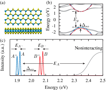
In this Letter we present a microscopic theory of excitonic effects in monolayer TMDs that describe the main features shown in Fig. 1 remarkably well. Our theory is based on two-body and three-body excitonic Hamiltonians in the effective mass approximation with screened interactions appropriate for strictly 2D semiconductors. The Hamiltonians are parametrized by ab initio calculations. Variational wavefunctions, inspired by previous treatments of excitons in semiconductor quantum wells [16, 17, 18], are employed. By treating neutral and charged excitons on an equal footing, we achieve an internal consistency that yields accurate, nontrivial predictions for neutral excitons while also providing quantitative insight into the more complex trion species as well as trion binding energies that agree well with those inferred from experiment. Our theory yields exciton binding energies in good, overall agreement with recent ab initio calculations based on the Bethe-Salpeter equation for TMDs [19, 20, 21, 22]. Extension of those calculations to the three-body trion problem is expected to be quite challenging.
Within the effective mass approximation, , our theory employs the neutral excitonic Hamiltonian
| (1) |
and trion Hamiltonian
| (2) |
the latter of which is a generalization of the familiar Hamiltonian for the negative hydrogen ion [23] or for trions in quasi-2D quantum wells [16, 17, 18]. It implicitly assumes that the trion can be treated as an isolated, three-body problem reached in the low doping limit 11 1 This approximation of isolated trions may be justified in the low doping limit due to disorder induced localization of carriers on lengthscales comparable to the exciton and trion radii.. This approximation precludes the observation of Fermi edge effects arising from the dynamical response of the electron gas [25, 15], an effect which has been observed in the absorption spectra of MoS2 [10]. We also neglect interband mixing, due to the large spin-orbit splitting in TMDs, and consider only the exciton and and its associated trion feature (see Fig. 1(c)); the features could be treated analogously. We also neglect any intervalley (–) coupling under the assumption of a selective, circularly polarized excitation [5, 6, 7]. The use of linear polarization can excite coherent superpositions of valley excitons, inducing a valley exchange interaction [12], also not treated here.
In typical experiments, the monolayer TMD material is surrounded by an environment with dielectric constants (above) and (below), but the electron and hole are restricted to orbitals that are primarily made up of TM -states at the center of the trilayer TMD unit. When there is a large dielectric contrast, which is typical of monolayer TMDs in vacuum or on weak dielectrics, the effective in-plane 2D interaction for charges separated by reduces to a form derived by Keldysh [26],
| (3) |
where and are the Struve function and the Bessel function of the second kind. This interaction behaves like a screened Coulomb potential at long range, but has a weaker logarithmic divergence at short range, where the crossover is determined by the screening length . The above interaction follows for a geometry which assumes the monolayer material has a thickness and isotropic dielectric constant , for which the screening length is given by . In the strictly 2D limit of a polarizable plane in vacuum (), Cudazzo et al. have recently rederived Eq. (3), showing that the screening length is given by , where is the 2D polarizability of the planar material [27]. For the case of surrounding vacuum, we have numerically verified that the screening length often times can be accurately calculated using either definition of , vide infra, assuming that the relevant dielectric constant of the monolayer is the in-plane component of the dielectric tensor of the bulk material. Here, we focus on freestanding monolayer TMDs, but in future work on monolayer TMDs in novel environments, the more general treatment of screening will be needed.
The necessary parameters for the exciton and trion Hamiltonians can be calculated from first principles. The effective masses can be extracted from the low energy band structure (see Fig. 1(b)), calculated in density functional theory (DFT) or the approximation [28]. To extract the 2D polarizability, and thus the screening length , we modify the protocol in Ref. 27 slightly. We employ the relation
| (4) |
where is the interlayer separation for a supercell containing two AB-aligned monolayers of TMD separated by vacuum. The in-plane dielectric constant is the limit of the head of the inverse dielectric tensor, calculated within the random phase approximation (RPA) [29]. Our protocol naturally interpolates between bulk TMDs ( where is the lattice constant) and monolayer TMDs (). This procedure tests the extraction of the monolayer 2D polarizability from the bulk dielectric constant via Eq. (4) retaining only the term of order .
We study four monolayer TMDs: MoS2, MoSe2, WS2, and WSe2. The effective mass of the electron and hole were calculated based on the parametrized band structures of Xiao et al. [5]. The Hamiltonian adopted in that work includes terms up to first order in , yielding identical electron and hole masses. Higher order terms in predict differing effective masses [30, *kor13], as also found in ab initio calculations [32, 19, 33, 22]. For evaluation of the polarizability, DFT and subsequent RPA calculations were performed with the quantum espresso [34] and berkeleygw [35] packages, respectively. For MoS2, in addition to the RPA result obtained with DFT input, we have also calculated the RPA dielectric constant with an approximate input, obtained by applying an -dependent rigid shift to the unoccupied DFT bands, , with eV and eVÅ, based on the results of Ref. 20. Further computational details appear in the Supplemental Material.
Using MoS2 as an example, Fig. 2 shows the calculated dielectric constant and the two-dimensional polarizability as a function of the interlayer separation employed in the supercell calculations. The dielectric constant clearly follows Eq. (4), giving the trivial limit of unity in the limit. Many studies utilize similar 3D supercells to calculate dielectric properties for 2D monolayer materials [36, 37, 33, 19]. Two reported values for MoS2 [37, 33] are plotted in Fig. 2(a), showing agreement with the present results. Clearly, the dielectric constant at a fixed supercell size together with an effective screened Coulomb interaction does not represent dielectric screening in monolayer TMDs. Furthermore, use of the conventional, 3D Wannier-Mott theory with such a model to estimate exciton binding energies or radii [33, 19] is not physical. In contrast, the two-dimensional polarizability shown in Fig. 2(b) converges to a finite and physically meaningful value independent of the final supercell size 22 2 The convergence of the polarizability is much slower due to the changing bandgap and required a extrapolation to the monolayer limit.. Specifically, we find Å and 5.0 Å, for DFT and , respectively. These values imply a two-dimensional screening length of 30–40 Å. To elucidate trends across materials, we use the DFT+RPA value and discuss the impact of the smaller polarizability below. Interestingly, we see that the DFT polarizability extracted from bulk MoS is extremely close to its converged monolayer value, showing the near-equivalence of the two previously discussed definitions of screening length, .

As a first approximation to the neutral excitonic properties of monolayer TMDs, we employ the total exciton wavefunction , where and are conduction and valence Bloch wavefunctions, with a simple variational guess for the envelope function,
| (5) |
This variational wavefunction becomes the exact ground state wavefunction in the limit of weak screening, where . For a nonzero polarizability, the wavefunction is no longer exact, but will exhibit the correct asymptotic behavior, i.e. exponential decay for distances larger than the screening length . For this wavefunction, the kinetic energy is easily shown to be and the potential energy is readily evaluated by quadrature. The exciton binding energy is then found by minimizing , where the optimum value of is an estimate of the exciton radius.
For the trion envelope wavefunction, we consider the simple variational form
| (6) |
a symmetrized product of exciton wavefunctions. First proposed by Chandrasekhar [39], it is perhaps the only two-parameter wavefunction to correctly predict a bound state of the negative hydrogen ion [23]. The differing exciton radii, , essentially allows one electron to sit close to the hole, near the neutral exciton radius, while the other is further away to minimize the unfavorable electron-electron repulsion. A polarization term can also be included, although we will not do so here for simplicity. For such a variational wavefunction, Eq. (6), with no dependence on the distance between the two electrons, the so-called Hughes-Eckart term vanishes [40], simplifying the numerical calculations. Again, the kinetic energy can be evaluated analytically and the potential energy can be calculated numerically as a three-dimensional integral.
The results for all four TMDs considered in this work are summarized in Table 1. Exciton binding energies are all predicted to be around 0.5 eV, with the ordering MoS2 WS2 MoSe2 WSe2. This trend generally agrees with recent ab initio Bethe-Salpeter equation (BSE) calculations on the same four materials [19]. Specifically for MoS2, we find a binding energy of 0.54 eV and an exciton radius of 10.4 Å. Four recent BSE studies [19, 20, 21, 22], which vary in details of implementation, give results that vary by a factor of two, falling between 0.5 and 1.1 eV (Table 1). Two technical challenges need to be fully resolved: convergence with respect to Brillouin zone sampling and the extrapolation of the results to limit, a particular challenge for the results [20]. Self-consistency would reduce screening, as is evident in Fig. 2. If we use our polarizability in the monolayer limit, we find a correspondingly larger binding energy of about 0.7 eV. It is common for DFT to overestimate polarizability, and so taken together, our variational estimates predict an exciton binding energy between 0.5 and 0.7 eV. All things considered, our variational estimate for the exciton binding energy is in good agreement with available ab initio calculations.
| Exciton binding energy | Trion binding energy | |||||
|---|---|---|---|---|---|---|
| Theory | BSE | Theory | Exp | |||
| MoS2 | 0.25 | 6.60 | 0.54 | 1.03, 1.1 [19, 20] | 26 | 18 [10] |
| 0.5, 0.54 [21, 22] | ||||||
| MoSe2 | 0.27 | 8.23 | 0.47 | 0.91 [19] | 21 | 30 [11] |
| WS2 | 0.16 | 6.03 | 0.50 | 1.04, 0.54 [19, 22] | 26 | |
| WSe2 | 0.17 | 7.18 | 0.45 | 0.90 [19] | 22 | 30 [12] |
Carrying out the variational minimization of for MoS2, we find a trion binding energy (defined as the difference between the trion and exciton variational energies) between 26 and 32 meV using the DFT and polarizability, respectively. These values are impressively close to the experimental value of 18 meV [10], suggesting that the approximations used here, including the form of the variational wavefunction, are accurate and physically meaningful. We find optimal radii of Å and Å, i.e. one electron is at the neutral exciton radius while the other is more than twice as far away, just as in the negative hydrogen ion. The largeness of this trion binding energy, which is almost exactly equal to thermal energy at room temperature, suggests that trions are intrinsically abundant and may play active roles in the excitonic physics of monolayer TMDs.
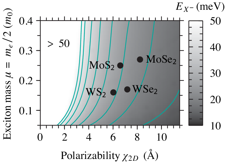
The calculated trion binding energies for all four TMDs studied fall in the range of 20–30 meV, in reasonable agreement with recently measured trion binding energies [10, 11, 12]. The similarity of trion binding energies in MoSe2 and WSe2 is perfectly reproduced. We find competing effects in the trion binding energy, parallel to the well-known trends for the exciton binding energy. As Fig. 3 shows, increase in effective mass or reduction in polarizability both lead to stronger trion binding. The exciton mass is largely determined by the metal (i.e. W versus Mo electrons) whereas the polarizability depends on both the metal and the chalcogen: selenides have larger polarizabilities than sulfides, and within a given chalcogenide family, molybdenum yields larger polarizabilities than tungsten. This argument also predicts a larger trion binding energy in MoS2 than in MoSe2, contrary to the limited experimental results to date [10, 11]. However, while the experiments on MoSe2 and WSe2 were done almost identically, the experiments on MoS2 required significant gating to achieve charge neutrality and exhibited extensive broadening in the lineshapes, both argued to be artifacts of defects introduced by mechanical exfoliation [10]. Definitive trends for intrinsic trion binding energies remain an ongoing challenge for both theory and experiment 33 3 We have also investigated the use of Eq. (3) with and to simulate the SiO2 dielectric substrate in experiments. This approach yields a trion binding energy in much better agreement with experiment for MoS2 but binding energies which are significantly underestimated for MoSe2 and WSe2. However, due to imperfect monolayer-substrate contact geometries, any intermediate vacuum spacing will reduce the effective dielectric constant of the environment..
We briefly consider the positive trion. Its Hamiltonian is identical to Eq. (2), except that the electron mass replaces the hole mass in the Hughes-Eckart term. Since this term vanishes for our choice of wavefunction, we predict the positive trion binding energy to be identical to that of the negative trion. More generally, any difference in the electron and hole masses only affects the binding energy to the extent that the true wavefunction depends explicitly on the distance between the electrons (for ) or between the holes (for ). This simple result may explain the equivalent positive and negative trion binding energies recently observed in monolayer MoSe2 [11], although more recent results on WSe2 exhibit asymmetric trion binding energies [12].
While our variational approach has proved very effective, particularly to elucidate trends in the trion binding energies, several physical effects remain to be quantified. A non-variational treatment will obviously increase the neutral exciton binding energy. Although we have neglected the repulsive electron-hole exchange interaction, which would decrease the binding energy, the relatively large exciton radius suggests that this contribution will be small. The trion binding energy, being an energy difference, is presumably less sensitive to these effects, such that a favorable cancellation of errors is likely responsible for the observed accuracy as compared to recent experiments. This latter effect is apparent in comparing binding energies based on DFT and polarizabilities: while the exciton binding energy increases by 40%, the trion binding energy only increases by 20%. Other atomic-scale factors include local fields in the screened interaction at shorter range, the role of the perpendicular extent of the electron and hole wavefunctions, and a more accurate treatment of the low-energy band structure that accounts for anisotropy in the effective mass and trigonal warping effects [30, *kor13].
To summarize, we have presented a simple, physically appealing theoretical treatment of both neutral and charged excitons in monolayers of TMDs, a family of prototypical two-dimensional semiconductors. Our results highlight the strong effective Coulomb interactions in monolayer TMDs and related 2D semiconductors that result in a dominant role for excitons in the low energy optical physics, including bound trions that may be further engineered to play a significant role at room temperature for device applications.
We thank Jens Kunstmann, Eran Rabani, Tony Heinz, and Louis Brus for invaluable discussions. This work was supported in part by the Center for Re-Defining Photovoltaic Efficiency through Molecule Scale Control, an Energy Frontier Research Center funded by the U.S. Department of Energy, Office of Science, Office of Basic Energy Sciences under Award Number DE-SC0001085. This work was carried out in part at the Center for Functional Nanomaterials, Brookhaven National Laboratory, which is supported by the U.S. Department of Energy, Office of Basic Energy Sciences under Contract No. DE-AC02-98CH10886 (M.S.H). T.C.B. was supported in part by the Department of Energy, Office of Science under Contract No. DE-AC05-06OR23100.
References
- [1] K. S. Novoselov, D. Jiang, F. Schedin, T. J. Booth, V. V. Khotkevich, S. V. Morozov, and A. K. Geim, Proc. Nat. Acad. Sci. 102, 10451 (2005).
- [2] K. F. Mak, C. Lee, J. Hone, J. Shan, and T. F. Heinz, Phys. Rev. Lett. 105, 136805 (2010).
- [3] A. Splendiani, L. Sun, Y. Zhang, T. Li, J. Kim, C.-Y. Chim, G. Galli, and F. Wang, Nano Lett. 10, 1271 (2010).
- [4] B. Radisavljevic, A. Radenovic, J. Brivio, V. Giacometti, and A. Kis, Nature Nanotech. 6, 147 (2011).
- [5] D. Xiao, G.-B. Liu, W. Feng, X. Xu, and W. Yao, Phys. Rev. Lett. 108, 196802 (2012).
- [6] H. Zeng, J. Dai, W. Yao, D. Xiao, and X. Cui, Nature Nanotech. 7, 490 (2012).
- [7] K. F. Mak, K. He, J. Shan, and T. F. Heinz, Nature Nanotech. 7, 494 (2012).
- [8] Y.-H. Lee, X.-Q. Zhang, W. Zhang, M.-T. Chang, C.-T. Lin, K.-D. Chang, Y.-C. Yu, J. T.-W. Wang, C.-S. Chang, J.-L. Li, and T.-W. Lin, Adv. Mater. 24, 2320 (2012).
- [9] A. M. van der Zande, P. Y. Huang, D. A. Chenet, T. C. Berkelbach, Y. You, G.-H. Lee, T. F. Heinz, D. R. Reichman, D. A. Muller, and J. C. Hone, Nature Materials (Article ASAP, DOI: 10.1038/nmat3633) (2013).
- [10] K. F. Mak, K. He, C. Lee, G.-H. Lee, J. Hone, T. F. Heinz, and J. Shan, Nature Materials 12, 207 (2013).
- [11] J. S. Ross, S. Wu, H. Yu, N. J. Ghimire, A. M. Jones, G. Aivazian, J. Yan, D. G. Mandrus, D. Xiao, W. Yao, and X. Xu, Nature Communications 4, 1474 (2013).
- [12] A. M. Jones, H. Yu, N. J. Ghimire, S. Wu, G. Aivazian, J. S. Ross, B. Zhao, J. Yan, D. G. Mandrus, D. Xiao, W. Yao, and X. Xu, arXiv:1303.5318 .
- [13] K. Kheng, R. T. Cox, Y. Merle d’Aubigné, F. Bassani, K. Saminadayar, and S. Tatarenko, Phys. Rev. Lett. 71, 1752 (1993).
- [14] G. Finkelstein, H. Shtrikman, and I. Bar-Joseph, Phys. Rev. Lett. 74, 976 (1995).
- [15] V. Huard, R. T. Cox, K. Samindayar, A. Arnoult, and S. Tatarenko, Phys. Rev. Lett. 84, 187 (2000).
- [16] B. Stébé, G. Munschy, L. Stauffer, F. Dujardin, and J. Murat, Phys. Rev. B 56, 12454 (1997).
- [17] B. Stébé, E. Feddi, A. Ainane, and F. Dujardin, Phys. Rev. B 58, 9926 (1998).
- [18] A. Esser, E. Runge, R. Zimmermann, and W. Langbein, Phys. Rev. B 62, 8232 (2000).
- [19] A. Ramasubramaniam, Phys. Rev. B 86, 115409 (2012).
- [20] H.-P. Komsa and A. V. Krasheninnikov, Phys. Rev. B 86, 241201(R) (2012).
- [21] J. Feng, X. Qian, C.-W. Huang, and J. Li, Nature Photonics 6, 866 (2012).
- [22] H. Shi, H. Pan, Y.-W. Zhang, and B. I. Yakobson, Phys. Rev. B 87, 155304 (2013).
- [23] H. A. Bethe and E. E. Salpeter, Quantum Mechanics of One- and Two-Electron Atoms (Plenum Publishing Corporation, 1977).
- [24] This approximation of isolated trions may be justified in the low doping limit due to disorder induced localization of carriers on lengthscales comparable to the exciton and trion radii.
- [25] P. Hawrylak, Phys. Rev. B 44, 3821 (1991).
- [26] L. V. Keldysh, JETP Lett. 29, 658 (1979).
- [27] P. Cudazzo, I. V. Tokatly, and A. Rubio, Phys. Rev. B 84, 085406 (2011).
- [28] M. S. Hybertsen and S. G. Louie, Phys. Rev. B 34, 5390 (1986).
- [29] M. S. Hybertsen and S. G. Louie, Phys. Rev. B 35, 5585 (1987).
- [30] H. Rostami, A. G. Moghaddam, and R. Asgari, arXiv:1302.5901 .
- [31] A. Kormanyos, V. Zolyomi, N. D. Drummond, P. Rakyta, G. Burkard, and V. I. Fal’ko, arXiv:1304.4084 .
- [32] H. Peelaers and C. G. Van de Walle, Phys. Rev. B 86, 241401(R) (2012).
- [33] T. Cheiwchanchamnangij and W. R. L. Lambrecht, Phys. Rev. B 85, 205302 (2012).
- [34] P. Gianozzi, et al., J. Phys. Condens. Matter. 21, 395502 (2009).
- [35] J. Deslippe, G. Samzonidze, D. A. Strubbe, M. Jain, M. L. Cohen, and S. G. Louie, Comput. Phys. Commun. 183, 1269 (2012).
- [36] M. van Schilfgaarde and M. I. Katsnelson, Phys. Rev. B 83, 081409(R) (2011).
- [37] A. Molina-Sánchez and L. Wirtz, Phys. Rev. B 84, 155413 (2011).
- [38] The convergence of the polarizability is much slower due to the changing bandgap and required a extrapolation to the monolayer limit.
- [39] S. Chandrasekhar, Astrophys. J. 100, 176 (1944).
- [40] H. Hogaasen, J.-M. Richard, and P. Sorba, Am. J. Phys. 78, 86 (2010).
- [41] We have also investigated the use of Eq. (3) with and to simulate the SiO2 dielectric substrate in experiments. This approach yields a trion binding energy in much better agreement with experiment for MoS2 but binding energies which are significantly underestimated for MoSe2 and WSe2. However, due to imperfect monolayer-substrate contact geometries, any intermediate vacuum spacing will reduce the effective dielectric constant of the environment.
- [42] J. P. Perdew, K. Burke, and M. Ernzerhof, Phys. Rev. Lett. 77, 3865 (1996).
I Supplemental Material
II Computational details
DFT calculations were performed with the quantum espresso [34] software package, using a -point grid with between 3 (for bulk) and 1 (for monolayer), using the exchange-correlation functional of Perdew, Burke, and Ernzerhof [42], norm-conserving pseudopotentials, and a plane-wave cutoff of 40 Ry ( 550 eV). RPA calculations were done with the berkeleygw [35] package on the same -point grid and included 50 unoccupied bands. The size of the dielectric matrix is determined by where the cutoff energy is equal to the energy of the highest unoccupied band included. The limit is taken numerically with a slightly shifted -point grid as described in Ref. 35.
For all materials studied, we employed experimental lattice constants and metal-chalcogen separations as given in Table 2.
| (Å) | (Å) | (Å) | |
|---|---|---|---|
| MoS2 | 3.16 | 12.30 | 1.59 |
| MoSe2 | 3.30 | 12.94 | 1.67 |
| WS2 | 3.16 | 12.35 | 1.59 |
| WSe2 | 3.29 | 12.98 | 1.67 |
III Macroscopic dielectric constants of bulk MoS2
Unlike in the case of monolayer systems, the static dielectric constant is well-defined for bulk TMDs. Using the procedure described in the text, we have calculated the transverse and longitudinal dielectric constant of bulk MoS2 as an example. These values are reported in Table 3 and compared to other recent values found in the literature.