Radiation induced electronic trap states and local structural disorder in van der Waals bonded semiconductor crystals
Abstract
In controlled X-ray irradiation experiments, the formation of trap states in the prototypical van der Waals bonded semiconductor Rubrene is studied quantitatively for doses up to (). About electronic trap states, located around above the valence band, are created by each absorbed photon which is 2–3 orders of magnitude more than protons produce. Thermal annealing is shown to reduce these traps. Local structural disorder, which has also been induced by other means in different studies, is thus identified as a common origin of trap states in van der Waals bonded molecular organic semiconductors.
Keywords:
CHARGE-LIMITED CURRENT; SINGLE-CRYSTAL; TRANSPORT; MOBILITY; ENERGY; X-RAY; TRAP STATE; ORGANIC SEMICONDUCTORpacs
71.20.Rv 72.80.LeThe understanding of charge traps in van der Waals bonded semiconductors has reached new levels in recent years and organic electronic devices’ performance has much improved with promising perspectives for applications. With the emerging understanding and spectral analysis of the trap density of states (DOS) [1, 2] it is highly desirable to quantify the interaction of environmental influences with van der Waals bonded semiconductors in terms of density and spectral distribution of the induced trap states. Such environmental influences may occur during fabrication, storage or operation of an organic electronic device. They cover a broad range of chemical [3], mechanical [4] and also radiative [5, 6, 7] phenomena.
The commonly known adverse influence of traps on charge transport [2] as well as spin diffusion length [8] is contrasted by an unexpected positive influence of X-ray radiation in electron-beam evaporation processes on the magnetotransport in organic materials [8]. These observations are a strong motivation to further investigate the defects arising from X-ray radiation.
Furthermore, after intense scintillation studies in the 1970s [9, 10, 11, 12], organic materials are considered anew for direct X-ray detection through the photoconductivity effect [6, 13]. For applications in low-cost, large-area integrated X-ray imaging panels it will be of central importance to assess the radiation damage and whether those defects can be healed by thermal annealing.
In this study we address the formation of electronic trap states upon X-ray irradiation in Rubrene single crystals, a grain boundary free model material for van der Waals bonded semiconductors. The spectral density of trap states (DOS) is determined by measuring current voltage characteristics at different temperatures and applying temperature-dependent space-charge limited current spectroscopy (TD-SCLC). The basic concept of SCLC is electrical transport by charge carriers thermally excited above a certain energy separating extended from localised states. No further a priori assumptions — in particular no specific transport model — are required. Due to the Fermi-Dirac statistics this excitation from localised traps to delocalised conducting states takes place in a small energy window. With increasing voltage, more space charge is injected, hence the Fermi energy is shifted towards the delocalised states. The trap DOS is calculated from this differential increment. The energy scale is given by the thermal activation energy at a given voltage corrected by the statistical shift, which accounts for the asymmetry of the DOS around . The full procedure is formally discussed in references 14, 15, 16, 17, 18, 19 and numerically implemented using cubic smoothing splines [20].
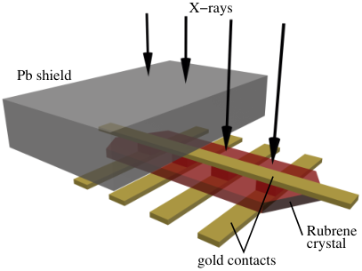
Rubrene crystals were grown by physical vapour transport in high purity argon flow. The platelet-like crystals were then laminated onto prefabricated gold electrodes, similar to the ‘flip-crystal’ technique [21]. For the vacuum deposition of the top electrode, the samples were cooled in order to minimise the thermal load on the crystals. The sample layout is schematically shown in Fig. 1. Current flows along the long crystallographic axis [22, 23, 24]. The simultaneous measurement of up to four sites on the same crystal — called channels — provides verifiable results and the shielding of some of these channels during irradiation provides the necessary reference. Furthermore, this sample arrangement (c.f. Fig. 1) enables checking of reproducibility and device stability.
The SCLC measurements were performed in darkness in a cryostat’s helium atmosphere. Charge carrier injection from the laminated bottom electrodes turned out to be more efficient than from the deposited top electrode and thus the polarity for all measurements was chosen accordingly. Current and power limits prevent crystal damage [25, 26] or local heating.
For the quantitative study of the radiation damage, a crystal diffractometer served as a well-defined monochromatic CuK () radiation source. The lateral intensity distribution (beam profile) was measured with the diffractometer’s image-plate detector and suitable Zirconium attenuators. For the measurement of the intensity in absolute units, a suitably calibrated instrument was kindly provided by the University Hospital Zurich. The beam’s peak intensity was corresponding to a photon flux of . Approximating Rubrene as a 42:28 mixture of carbon and hydrogen the crystal at the center of the beam absorbed a dose of () [27] during one hour of exposure. The thick gold top contact absorbs only about of the incident intensity. For comparison, a single computed tomography (CT) scan accounts for up to [28], typical radiotherapy doses are some [29] and the accumulated lifetime dose of X-ray imaging sensors is a few [13].
After first measuring the trap DOS of the pristine crystals, the samples were transfered to an Argon filled glass tube with a Kapton window and aligned in the X-ray beam with fluorescent marks. During irradiation, two out of four channels were shielded by a lead foil thus providing reference data on the same crystal. After each hour of irradiation, the samples were measured and the trap DOS calculated. These repeated measurements required the crystals to be stable over multiple thermal cycles between and .
The densities of states measured on two crystals before and after irradiation are shown in Fig. 2. The unirradiated channels do not show any significant change in the trap DOS compared to the pristine state — an example is shown for crystal B. Thus, X-ray induced defects are clearly identified. Furthermore, the unchanged DOS in unirradiated channels reflects the stability and reproducibility of sample handling and measurement.
In the exposed channels, the trap DOS increases by up to (Fig. 2, crystal B) in a narrow energy range peaked around . The area under this peak yields the total trap density of traps generated during one hour of X-ray irradiation. After the second hour of irradiation, the induced trap density has doubled within experimental uncertainty. The X-ray absorption length is much longer than the typical crystal thickness of (only of the photons are absorbed), and with an hourly dose of , approximately photons are abosrbed per creating a uniform defect density.
To quantitatively compare X-ray and ion irradiation in Fig. 3 it is appropriate to consider the microscopic interaction mechanism as sketched in the insets. An absorbed X-ray photon will deposit its full energy of in a single primary event causing a cascade of secondary events which in turn create numerous microscopic defects. In contrast, every proton of experiences approximately primary interactions on its way through a thick crystal, each time transfering to the crystal’s electronic system [7, 30]. Simulations using the same SRIM [31] parameters as in ref. 7 show that atom displacement is negligible.
The electronic excitations allow for hydrogen atoms to be detached from Rubrene molecules [32]. They will then diffuse through the crystal and cause structural disorder as interstitials in the Rubrene lattice. Since the crystal surfaces in this study were not covered during irradiation, it was possible for detached hydrogen to escape from the crystal. It is thus appropriate to consider the open surface data from reference 7 (open symbols in Fig. 3) for a comparison.
The density of radiation-induced traps is plotted as a function of primary events in Fig. 3. Note that the primary event counts of the X-ray datapoints are an upper limit based on the assumption that the samples were centred at peak intensity. Solid blue (proton radiation) symbols are data from covered surfaces saturating at high dose due to re-attachement of hydrogen knocked off in a previous event. For each primary interaction event, protons create , while X-rays produce . A central result of this study is: per primary interaction event, X-rays are found to be times more effective than ions in trap generation. This is attributed to the shower of secondary events following every photon absorption. These showers spatially distribute the energy in the crystal as opposed to the point-like event of an ion interaction. These secondary events apparently carry enough energy to create defects and their number would account for the 100- to 1000-fold defect creation rate.
The spectral distribution of the additional traps suggests their common microscopic origin: they are peaked above the (hole) mobility edge and the peak is wide. The summary in Fig. 4 shows data for Rubrene crystals irradiated with protons or Helium ions [7], together with X-ray data from this study. Most remarkably, a very similar position and distribution width has been found in Pentacene thin films exposed to oxygen [33] and in UV/ozone exposed Rubrene single crystals [3]. Furthermore, recent low background UPS studies [34] also report the formation of energetically very similar traps when oxygen but also chemically neutral nitrogen or argon penetrate Pentacene films and the same defects have been found in both photocurrent measurements in organic solar cells[35] and density functional calculations of specific hydrogen- and oxygen-related defects[36, 37].
To further elucidate the origin of radiation induced trap states, Crystal A in Fig. 2 has been annealed for at in helium atmosphere. Most significantly, a reduction of radiation defects by approximately is observed. This is a central result and is in line with previous observations in anthracene crystals [38, 11, 39].
A motivation to consider structural defects as a possible cause is the partial recovery after thermal annealing at moderate temperatures. Annealing of structural defects even at room temperature has been shown to take place in Pentacene thin films always kept in high vacuum [40]. Similarly, intercalation with inert gases (N2 and Ar) induces trap states at a similar energy [34]. Also in organic polymer solar cells, radiation induced damage recovering by annealing has been observed and interpreted in terms of hydrogen detachment and rearrangement [35, 37, 41]. Particularly interesting is the bending of a pentacene molecule when two hydrogen atoms are attached to the initially flat entity, creating localised electronic states [36]. Similar detailed calculations for Rubrene [42] with attached oxygen of hydrogen in various configurations give no evidence for new electronic states within the few tenths of above the HOMO band accessible in the experiment. However, they reveal a slight rotation of a phenyl side-group. While the authors are not aware of a corresponding calculation involving a missing hydrogen in Rubrene, the previous experimental observations [7] clearly suggest hydrogen detachment to be a key step in trap state formation.
The discussion about the microscopic nature of intentionally induced defect states in organic semiconductor crystals is now stimulated by (a) the formation of electronically active states above the HOMO band and (b) the ability to partially anneal them at very moderate temperatures. Future studies therefore might address the relative impact of new chemical species perturbing the electron system (e.g. H detachment, O or OH attachement), and on modifications of the molecule’s structure and its environment in the crystal. Combining local probes and macroscopic transport measurements will produce such new insights.
In conclusion, we have quantitatively studied the formation of bulk trap states in van der Waals bonded single crystals by X-ray irradiation. For each absorbed photon, approximately trap states are created, while proton irradiation [7] generates up to trap state per primary interaction. The spectral trap distribution is peaked near above the HOMO transport level and is wide. Very similar trap distributions which can be partially annealed are produced by hydrogen- and oxygen-related chemical defects but also when van der Waals bonded semiconductors are locally disturbed by proton or Helium ion radiation [7] or by penetration of oxygen or chemically neutral nitrogen or argon [3, 33, 2, 34]. This formation of energetically very similar trap states by a wide range of treatments and the observation of partial annealing of these states set the framework for future studies focussing in the respective contributions of chemical and structural defects.
Acknowledgements.
The authors thank Carlo Bernasconi from the Laboratory of Crystallography, ETH Zurich for access to the X-ray diffractometer. Stephan Klöck and Jérôme Krayenbühl from University Hospital Zurich are greatfully acknowledged for their help in measuring the X-ray intensity and Kurt Mattenberger for support with various technical issues.References
- [1] A. Salleo, Electronic Traps in Organic Semiconductors (Wiley-VCH Verlag GmbH & Co. KGaA, 2013), chap. 14, pp. 341–380, ISBN 9783527650965.
- [2] W. L. Kalb, S. Haas, C. Krellner, T. Mathis, and B. Batlogg, Phys. Rev. B 81, 155315 (2010).
- [3] C. Krellner, S. Haas, C. Goldmann, K. Pernstich, D. Gundlach, and B. Batlogg, Phys. Rev. B: Condens. Matter Mater. Phys. 75, 245115 (2007).
- [4] T. Sekitani, Y. Kato, S. Iba, H. Shinaoka, T. Someya, T. Sakurai, and S. Takagi, Appl. Phys. Lett. 86, 073511 (2005).
- [5] A. Quaranta, A. Vomiero, S. Carturan, G. Maggioni, and G. Della Mae, Synth. Met. 138, 275 (2003).
- [6] C. R. Newman, H. Sirringhaus, J. C. Blakesley, and R. Speller, Appl. Phys. Lett. 91, 142105 (2007).
- [7] T. Zimmerling, K. Mattenberger, M. Döbeli, M. J. Simon, and B. Batlogg, Phys. Rev. B 85, 134101 (2012).
- [8] J. Rybicki, R. Lin, F. Wang, M. Wohlgenannt, C. He, T. Sanders, and Y. Suzuki, Phys. Rev. Le 109, 076603 (2012).
- [9] S. Weisz, A. Cobas, P. E. Richardson, H. H. Szmant, and S. Trester, J. Chem. Phys. 44, 1364 (1966).
- [10] J. Birks, Proc. Phys. Soc. A 64, 874 (1951).
- [11] K. Yokoi and Y. Ohba, Chem. Phys. Lett. 56, 560 (1978).
- [12] N. Shiomi, J. Phys. Soc. Jpn. 23, 1177 (1967).
- [13] J. Blakesley, P. Keivanidis, M. Campoy-Quiles, C. Newman, Y. Jin, R. Speller, H. Sirringhaus, N. Greenham, J. Nelson, and P. Stavrinou, Nucl. Instrum. Methods Phys. Res., Sect. A 580, 774 (2007).
- [14] O. Zmeškal, F. Schauer, and S. Nešpůrek, J. Phys. C: Solid State Phys. 18, 1873 (1985).
- [15] F. Schauer, S. Něspůrek, and O. Zmeškal, J. Phys. C: Solid State Phys. 19, 7231 (1986).
- [16] F. Schauer, S. Něspůrek, and H. Valerián, J. Appl. Phys. 80, 880 (1996).
- [17] F. Schauer, R. Novotny, and S. Nešpůrek, J. Appl. Phys. 81, 1244 (1997).
- [18] S. Nešpůrek, O. Zmeškal, and F. Schauer, Phys. Status Solidi A 85, 619 (1984).
- [19] D. Braga, N. Battaglini, A. Yassar, G. Horowitz, M. Campione, A. Sassella, and A. Borghesi, Phys. Rev. B 77, 115205 (2008).
- [20] C. de Boor, A practical guide to splines, vol. 27 of Applied mathematical science (Springer Verlag, New York, 1987).
- [21] J. Takeya, C. Goldmann, S. Haas, K. Pernstich, B. Ketterer, and B. Batlogg, J. Appl. Phys. 94, 5800 (2003).
- [22] O. D. Jurchescu, A. Meetsma, and T. T. Palstra, Acta Crystallogr., Sect. B: Struct. Sci. 62, 330 (2006).
- [23] E. Menard, A. Marchenko, V. Podzorov, M. E. Gershenson, D. Fichou, and J. A. Rogers, Adv. Mater. 18, 1552 (2006).
- [24] T. Minato, H. Aoki, H. Fukidome, T. Wagner, and K. Itaya, Appl. Phys. Lett. 95, 093302 (2009).
- [25] J. Srour, G. Vendura, D. Lo, C. Toporow, M. Dooley, R. Nakano, and E. King, IEEE T. Nucl. Sci. 45, 2624 (1998).
- [26] J. Srour, J. Palko, D. Lo, S. Liu, R. Mueller, and J. Nocerino, IEEE T. Nucl. Sci. 56, 3300 (2009).
- [27] J. Hubbell and S. Seltzer, Tables of x-ray mass attenuation coefficients and mass energy-absorption coefficients, URL http://physics.nist.gov/PhysRefData/XrayMassCoef/cover.html.
- [28] D. J. Brenner and E. J. Hall, N. Engl. J. Med. 357, 2277 (2007).
- [29] J. Krayenbühl, private communications.
- [30] M. Pope and C. E. Swenberg, Electronic processes in organic crystals and polymers (Oxford University Press, 1999).
- [31] J. Ziegler, J. Biersack, and U. Littmark, SRIM The Stopping and Range of Ions in Solids (Pergamon Press, New York, 1985), URL http://www.srim.org.
- [32] R. Barillon and T. Yamauchi, Nucl. Instrum. Methods Phys. Res., Sect. B 208, 336 (2003).
- [33] W. L. Kalb, K. Mattenberger, and B. Batlogg, Phys. Rev. B 78, 035334 (2008).
- [34] F. Bussolotti, S. Kera, K. Kudo, A. Kahn, and N. Ueno, Phys. Rev. Lett. 110, 267602 (2013).
- [35] R. Street, J. Northrup, and B. Krusor, Phys. Rev. B: Condens. Matter Mater. Phys. 85, 205211 (2012).
- [36] J. E. Northrup and M. L. Chabinyc, Phys. Rev. B 68, 041202(R) (2003).
- [37] J. E. Northrup, Applied Physics Express 6, 121601 (2013).
- [38] G. Heppell and R. Hardwick, Trans. Faraday Soc. 63, 2651 (1967).
- [39] C. Zorn, Nucl. Phys. B, Proc. Suppl. 32, 377 (1993).
- [40] W. L. Kalb, F. Meier, K. Mattenberger, and B. Batlogg, Phys. Rev. B: Condens. Matter Mater. Phys. 76, 184112 (2007).
- [41] K. Nakagawa and N. Itoh, Chem. Phys. 16, 461 (1976).
- [42] L. Tsetseris and S. Pantelides, Phys. Rev. B: Condens. Matter Mater. Phys. 78, 115205 (2008).