Anomalous transport in half-metallic ferromagnetic CrO2
Abstract
We have investigated transport properties of CrO2 thin films deposited on TiO2 and sapphire substrates. The films are good metals down to low temperatures. The residual resistivity is of the order of 6 cm for films deposited on TiO2 and two times higher for films on sapphire substrates. The sign of the magnetoresistance (MR) changes from negative to positive at a temperature around 100 K. This fact, as well as a rapid change in the ordinary and anomalous Hall coefficients suggest a change in the electronic state. At lower temperatures the MR is a linear function of the applied field. This linear dependence might be explained as intergrain tunneling MR. This interpretation is also suggested by the angular MR. The planar Hall effect measurements reveal that the CrO2 thin films are not in a single magnetic domain state even for films deposited on an isostructural TiO2 substrate.
I Introduction
The material CrO2 belongs to the class of half metallic ferromagnets (HMF) [1, 2], as revealed by electronic band structure calculations [3, 4] and point contact Andreev Spectroscopy (PCAS) [5, 6]; i.e. it has a gap in the minority-spin density of states (DOS) () at the Fermi level of the order of 1.5 eV, but no gap in the majority DOS (), resulting in complete spin polarization at the Fermi level. These findings have stimulated the interest in CrO2 as a source of spin-polarized electrons for spintronics devices. Also, its halfmetallic character was recently used for the realization of long-ranged supercurrents [7, 8, 9]. However, the electronic properties of CrO2 are still not fully understood. For instance, the resistivity between 10 K and 300 K is usually described in terms of an excitation gap [10, 11], but a clear connection with an electronic or spin gap excitation cannot be made. Also, different results have been reported with respect to the Hall effect. Watts et al. presented data showing a sign reversal at low temperatures [11], which they interpreted as evidence for two-band transport, but this was not found in later studies [12, 13]. In this article we return to the issue of magnetotransport in high-quality thin films of CrO2, with proper attention to the different crystallographic axes of the material. We find resistivity behavior which is subtly different from earlier reports, with an anomaly around 100 K. We do not see a sign change in the Hall effect, but we do find non-monotonous behavior in the high-field magnetoresistance. We also study the low-field magnetoresistance behavior and come to a similar conclusion as König et al., that Intergrain Tunneling Magnetoresistance (ITMR) takes over from Anomalous Magnetoresistance (AMR) when the temperature decreases to below 100 K. Data on the Planar Hall Effect (PHE) confirm that the magnetization does not switch in single-domain fashion in these films, different from one particular case reported by Gönnenwein [15]. The article consists of two parts. First, the measurements of the temperature-dependent resistance , of the high-field MR and of the Hall effect are presented and discussed. Next, the data on the low field magnetoresistance (MR) are given, with emphasis on the angular dependent MR and on the planar Hall effect. We conclude that the data indicate that a change in the electronic structure of CrO2 takes place around 100 K, possibly driven by a decrease of the carrier concentration.
II Material and sample preparation
CrO2 is a tetragonal material with a rutile structure and lattice parameters
= = 0.4421 nm and = 0.2916 nm. In CrO2, the oxygen atoms form
octahedra around the Cr-atoms. There are two inequivalent octahedra,
side-sharing and corner-sharing ones. The side-sharing octahedra form a kind of
ribbons along the -axis [16] (slightly distorted, elongation
along the -axis [4, 3]). The Cr ion in its formal 4+
valence state has two electrons in the orbitals with the spin quantum
number . As mentioned, CrO2 is a HMF, although a Mott insulating-like
ground state and antiferromagnetic spin order could be expected because of
strong correlations. Kroton et al. [4] showed using the
LSDA+U method that the bands of CrO2 are divided into two parts: a
weakly dispersing band well below the Fermi level and a strongly dispersing
band crossing the Fermi level. The former band provides the localized moments
and the latter is a strongly hybridized band that dilute the effect of
the Coulomb interaction and is responsible for the metallic behavior in
CrO2. The oxygen state extends to the Fermi level and plays the role
of electron or hole reservoirs. This causes self-doping and double-exchange
(DE) between the -electrons and is responsible for the half-metallic nature.
A strong correlation between the spins of localized and non-localized electrons
makes the Hall effect and also the anomalous Hall effect a subtle tool to probe
topological spin defects of the 3D ferromagnetic material
[12, 13].
The compound CrO2 is a metastable phase and bulk material is synthesized at
high pressures. Deposition techniques such as sputtering, pulsed laser
deposition or molecular beam epitaxy cannot be used, but high quality thin
films can be grown using the technique of chemical vapor deposition (CVD) at
ambient pressure, as for instance discussed in
Refs. [17, 18, 19, 20, 21, 22]. In CVD, a
precursor such as CrO3 is thermally evaporated at 260 ∘C and the
sublimated precursor transfers to a lattice matched substrate (such as
TiO2 or Al2O3) at an elevated temperature of 390 ∘C
using a pure Oxygen flow at 100 sccm. The lattice parameters of TiO2 (rutile
with = = 0.4594 nm, mismatch with TiO2 -3.8%; = 0.2958 nm,
mismatch -1.5%) closely match those of CrO2 and epitaxial growth is
possible with small (although not negligible) effects of substrate-induced
strain. The growth on an -axis oriented substrate is in the form of
rectangular grains with the long axis aligned along the film -axis and the
short axis along the -axis. It has been reported that pretreatment of the
TiO2 substrates with hydrofluoric acid (HF) can enhance the strain in the
films [22, 23, 24, 25] and it affects both magnetic and
electronic properties. Growth on sapphire is more complicated because of its
hexagonal structure ( = 0.4754 nm), which is close to Cr2O3. Growth on
sapphire actually starts with Cr2O3 and then changes to the required
CrO2 [20, 21]. Grains are aligned at 60∘ to each other
with six-fold rotational symmetry of hexagonal crystal structure of underlying
sapphire substrate. For details about film growth and morphology, see
Ref. [23]

To investigate transport properties of CrO2 thin films, microbridges were structured in the films deposited via the above mentioned CVD process on untreated TiO2, pretreated TiO2 and sapphire substrates. For films deposited on both pretreated and untreated TiO2 substrates, L-shaped bridges were fabricated in order to investigate the transport along both in-plane crystal directions (current along the - and -axis) at the same time. They were made with electron-beam lithography. The bridges were 40 m wide, with 200 m separation between the voltage contacts and 100 nm thickness of the film. For the lithography step, a negative resist (MaN2405) was spin coated at 4000 rpm for 60 sec, and baked for 10 min at 90 ∘C. Next, the L-structure was etched in the CrO2 films, a schematic is shown in Fig. 1. It is difficult to etch the film with Ar ion etching because of a rather slow etch rate. So, etching was done with reactive ion etching (RIE), where a mixture of CF4 (30 sccm) and O2 (15 sccm) was utilized with a background pressure of 10-6 mbar. The RIE etch rate was of the order of 0.8 nm/sec. For the sapphire substrate, a 200 nm thick film was grown, in which a Hall bar (200 m wide, 2 mm between the voltage contacts) was structured with optical lithography.
III Results: Resistivity, magnetoresistance, Hall effect
III.1 Resistivity
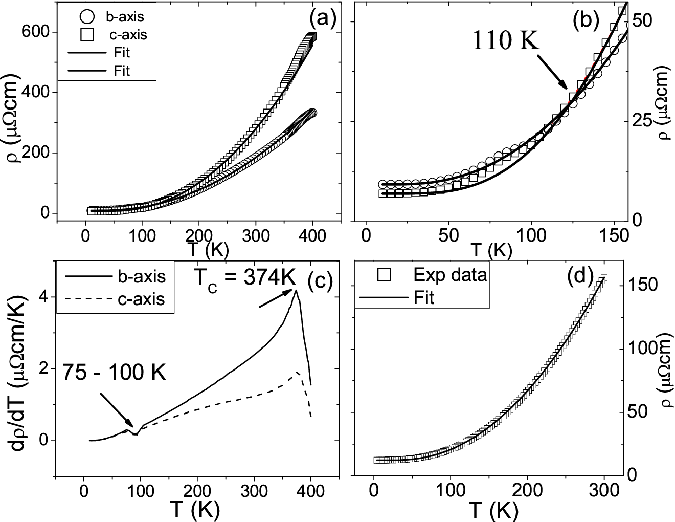
Figure 2a shows the resistivity as a function of temperature for a 100 nm thick CrO2 film deposited on a pretreated TiO2 substrate, along both the -axis and the -axis. The residual resistivity () is of the order of 9 cm along the -axis while along the -axis it is found 6 cm. These values are quite similar to the literature values [11, 12]. It is noticeable that at 4 K is lower for the -axis than for the -axis, while this tendency reverses at room temperature, with a crossover at 110 K (see Fig. 2b). We observed an unexpected bump in between 75 - 105 K along both in-plane axes that is very clear in the derivative of the resistivity plotted in Fig. 2c. The derivative also reveals the ferromagnetic transition at around 374 K. Qualitatively, the results are the same for CrO2 films deposited on untreated TiO2 and pretreated TiO2 substrates although there is rather a small quantitative difference.
Figure 2d presents data of a 200 nm thick CrO2 film deposited on a sapphire substrate. At low temperature, becomes almost temperature independent, with 12 cm, larger than of the films deposited on TiO2. In contrast, at room temperature, is significantly lower than those for films on TiO2.
| (1) |
where is a coefficient. As shown in Fig. 2 this expression fits the data well. Table 1 gives typical numbers for , and . The low values of indicate that the films behave as good metals at low temperatures. The mean free path can be estimated from the free electron model using the relation , where is the density of states at the Fermi level, is the Fermi velocity and is the charge of the electron. Using states/J/cm3 and m/s [3], is evaluated to be about 100 nm. This long suggests that the grain boundaries do not strongly affect the transport behavior. The values of are around 100 K, which does not seem to be related to a characteristic energy scale of the material. This will be discussed further below, but here we note that 100 K is the temperature where shows an anomaly.

As the physical significance of is not clear, we also tried to simply fit a behavior without the exponential term. The results are shown in Fig. 3(a,b). For the films deposited on TiO2, resistivity shows a quite good fit to the T2 dependence along the -axis between 100 K to 350 K, similar to the results of Suzuki et al. [30] for CrO2 film deposited on ZrO2 substrate. In contrast, along the -axis, the fit is quite poor and is only successful between 215 K and 312 K. This fact is related to the change in the anisotropic behavior of resistivity as a function of temperature.
| Samples | |||
| cm | (K) | ncm /K2 | |
| pretreated-TiO2 (-axis) | 6 | 80 | 2.8 |
| (-axis) | 9 | 150 | 5.2 |
| untreated-TiO2 (-axis) | 7 | 75 | 2.6 |
| (-axis) | 11 | 140 | 3.9 |
| sapphire | 12 | 90 | 2.2 |
III.2 Magnetoresistance: High field MR
Magnetoresistance (MR) is the measure of the relative change in the resistance of a material in an externally applied magnetic field at a constant temperature, and defined as
| (2) |
where is the resistance in zero field and is the resistance in the field. High-field MR was measured at different temperatures with a commercial apparatus (Quantum design, PPMS) with fields (maximum 9 T) oriented along the out-of-plane direction for CrO2 films deposited on both pretreated and untreated TiO2 substrates.
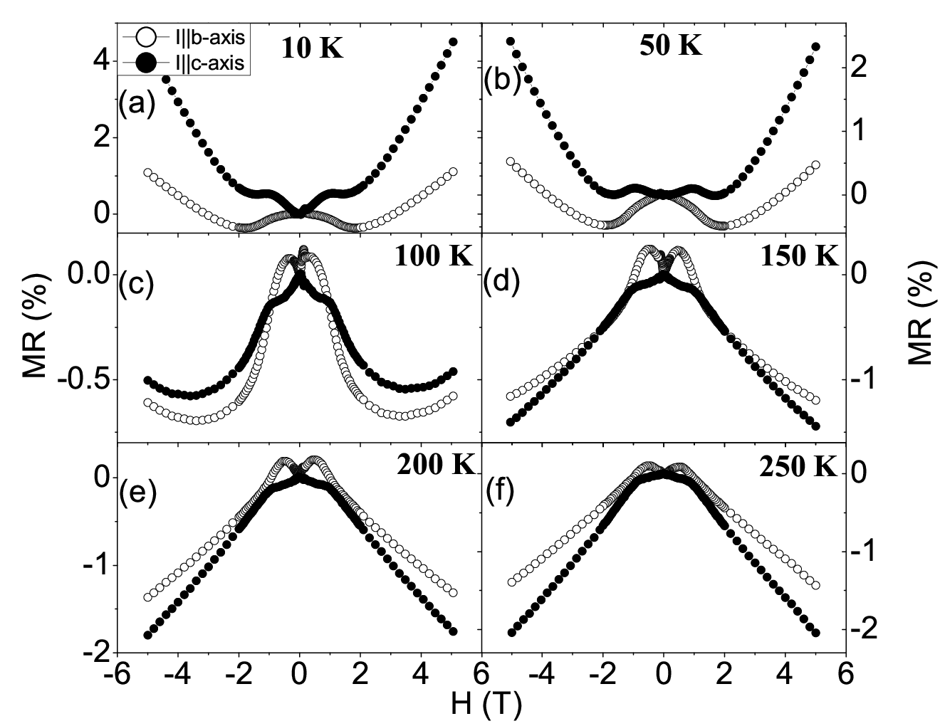

Figure 4 shows the data for MR measured at various temperatures between 10 K to 250 K for a 100 nm thick CrO2 film deposited on a pretreated TiO2 substrate. At low fields, the MR shows variations associated with the changes in the magnetization. When the magnetization saturates, above 1 T, monotonic behavior sets in. An interesting observations is that the slope of MR in high fields is different in sign for low temperatures and high temperatures, and that at temperatures below 150 K the crossover can be seen as function of field. Above 100 K, the MR is negative, with values around -2 at 5 T around room temperature (250 K). At 100 K, the sign is still negative but a cross-over to positive behavior is visible at about 4 T, where MR changes quadratically. At 50 K and 150 K, the MR starts to be negative, but reverses to positive around 2 T. At 10 K the MR reaches 4 (1) in 5 T with current along the -axis (-axis).We observed similar behavior for films on untreated TiO2, except that the lower field curves are not symmetric. This symmetry might be related to the quality of the films.
Figure 5 shows the MR for the 200 nm thick film on sapphire, again with the field applied to the out-of-plane direction. The data show the same features; positive MR at 10 K, a cross-over at 100 K, negative MR at 300 K. Noteworthy are the large values at 10 K, of the order of 30 at 8 T.
III.3 Anomalous Hall Effect
Figure 6a shows the Hall resistivity (where is the width of the Hall bar) as a function of externally applied field in out-of-plane configuration, for various temperatures between 10 K to 400 K, using the same L structure. The measurement was done for films deposited on both pretreated and untreated TiO2 substrates, and for current passing along both the - and the -axis. We did not observe any difference beyond the experimental error for both directions of current and for both kind of films, in agreement with Onsagers principle that regardless of crystal orientation.

At low temperatures (50 K), is linear with a slope that corresponds to hole-like charge carriers. Between 100 K and 350 K, an extra contribution is visible at low fields, which is usually ascribed to the effects of the magnetization, and referred to as the anomalous Hall effect (AHE).
The Hall resistivity can then be written as
| (3) |
with the normal Hall coefficient and the anomalous Hall coefficient.The carrier density follows in a one-band model from . A positive corresponds to holes as carriers.
IV Discussion
The discussion on the data given above can be started with . The different values of for different substrates indicates a substrate dependence of the film quality because is sensitive to the disorder. The ratio between room temperature resistivity and is a measure of the crystal imperfections or impurity concentration as electron-phonon scattering vanishes at low temperatures. This ratio is known as the residual resistance ratio (RRR) [29]. For our samples the RRR is 20 along the -axis and 41 along the -axis. These values are higher than those for the films deposited on an untreated TiO2 and sapphire substrates. This fact reveals that CrO2 films deposited on a pretreated TiO2 substrate are of better quality.
Another important issue is the description of with Eq. (1), which is usually interpreted as a contribution modified with a phenomenological exponential. In general, the term is attributed to electron-electron scattering. The value of the coefficient of the term is in the range of 2.2 - 5.0 10-3 cm/K2 and much larger than those for ordinary ferromagnetic metals (e.g. 1.3-1.6 10-5 cm/K2; for Ni, Fe) [30]. The higher value might be related to the contribution of the electron-magnon scattering along with electron-electron scattering [31, 30]. If also has electron-magnon scattering contributions then the prefactor of the exponential term might be related with a gap in magnon spectrum. However, the value of is found to be about 150 K (maximum, along the -axis), which is still too low to be associated with spin flip scattering, since the minority spin band is about 1.5 eV below the Fermi level. That suggests there is no correlation of with spin flip scattering in CrO2. It is remarkable that the value of falls in the temperature range of about 100 K where we find a dip in . This suggests a certain electronic phase change in CrO2 around 100 K. That is reinforced by the high-field MR data, which show a field dependent sign change around 100 K which was not observed in earlier work [11]. In contrast, we do not find a sign reversal in the Hall data, which allows us to extract a carrier density using a one-band model as shown in Fig. 6(c). The carriers are holes, and we find that their number actually is not constant: starts to drop significantly for temperatures below 200 K. There appears therefore to be no reason to try describing the resistivity in the whole temperature regime with a single expression. Something can also be said about the anomalous Hall coefficient , which is plotted in Fig. 6(d). Although is negligibly small below 100 K, it grows exponentially around 150 K and has a peak at 350 K, just below the Curie temperature. It is also interesting that the sign of and are different, since for conventional ferromagnets the signs are the same. The different sign is quite similar to what has been observed in Colossal Magnetoresistance materials such as (La0.7Sr0.3)MnO3 or (La0.7Ca0.3)MnO3 and they seem to rule out the conventional explanations of conventional spin scattering and side jump or skew scattering but a Berry phase might be the possible explanations for these materials. Recently, it was suggested that topological spin defects or Skyrmion strings [12, 32] can be an origin of the behavior of AHE, in particular for double exchange systems (also the case of CrO2 with self doped double exchange). The density of Skyrmion strings and are related as
| (4) |
V Results: Low field MR, Rotational scans of MR, Planar Hall Effect
V.1 Magnetoresistance: Low field MR
The low field MR was measured at 4.2 K with a cryostat (Oxford instruments metal shielded) with externally applied magnetic field with in-plane configuration. For the same samples used in above mentioned experiments, we applied field parallel and perpendicular to the current for both cases of current along the - and the -axis. The field was applied parallel to the current for the film deposited on sapphire with the Hall bar structure. For all cases, four probe dc measurements with a current of 100 A were used.
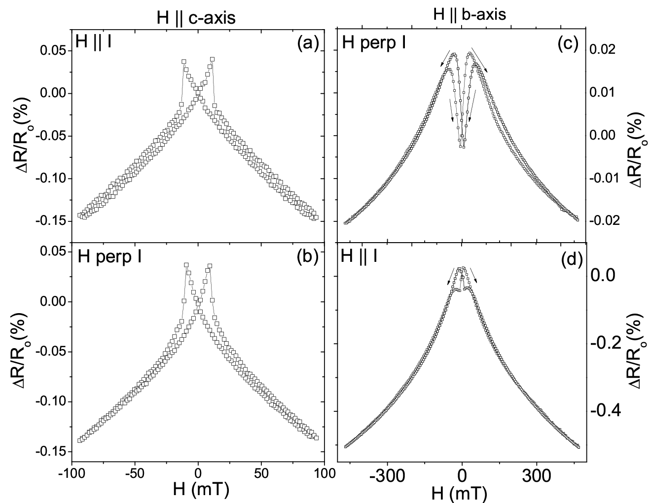
In all cases, the resistance increases when coming from high field, and shows a hysteretic structure when the magnetization direction switches and domain forms. When field is applied along the -axis (H) then for both H (or ) and H (or ) the data show a jump-like decrease of at the presumed coercive field (see Fig. 7(a)(b)). When the field is applied along the -axis (H) then the resistance for H (or ) exhibits a dip slightly above and a peak around (see Fig. 7c). For H (or ) a different structure is seen with a plateau slightly above and a peak at (see Fig. 7(d)).
The MR behavior was already studied by König et al. [14], with results similar to these. They interpreted their results assuming the -axis as easy axis; regardless of the angle between and , the magnetization switches sharply for H. For H domains start to form well above , which leads to a dip or a plateau in the variation of . For their sample, a magnetization measurement confirmed that the -axis is indeed the easy axis.

Figure 8(a) presents the low field MR data for a 200 nm thick CrO2 film deposited on a sapphire substrate for . The MR is negative with a sublinear decrease up to 0.25, which is similar to the MR data of CrO2 films deposited on TiO2 substrates for . The AMR peaks around the coercive field are obviously present (see the inset of Fig. 8(a)). The MR for the perpendicular configuration is two times less than the MR for the parallel configuration of applied field. The peaks at the coercive field are also very weak for (see Fig. 8(b)) but the decrease is still sublinear.
V.2 Rotational scans of MR
We also measured the MR as a function of the angle of the applied field with respect the -axis for and . We probed at different temperatures and also at various magnetic field strengths using a rotational sample holder of PPMS Quantum design. In Fig. 9, at different temperatures for 50 mT applied field is plotted. The data for both configurations of and are simultaneously recorded. At the applied field is along the -axis as shown in the inset of Fig. 9(b).


At 300 K, for is weakly varying, with signatures of maxima at 0∘, 180∘, and minima at 90∘, 270∘. For there is a clear variation with peak-like maxima at 90∘ and 270∘, and rounded minima at 0∘ and 180∘. At 200 K the data are similar, now with a stronger variation for . At 100 K the peaks become round somewhat, but there is no qualitative change. At 10 K, although, the data for are still similar, the data for exhibit strong difference: the minima at 90∘ and 270∘ have converted to sharply peaked maxima, similar to the data. The shape of the maxima, and the small hysteresis which can be seen to develop, are partly due to the relatively small applied field. For larger fields the MR-effect becomes stronger, and the maxima more rounded, as shown in Fig. 10 for at 4.2 K.
Also these observations are similar to earlier ones [14]. To understand what happens, we compare the 100 K data with the 10 K data. At 100 K the behavior can be explained with the -axis being the easy axis. It yields a maximum at 0∘ for H, since the magnetization is parallel to the current, which gives a higher . Also at 90∘, the configuration H gives domains with a magnetization perpendicular to the current, and therefore a minimum in . At 10 K the effect of the easy axis seems to have disappeared and the parallel alignment of magnetization and current (the situation H) now leads to minimum. This can be explained by assuming that the dominating transport mechanism is ITMR. The parallel alignment of the magnetization of neighboring grains reduces the scattering at grain boundaries. It is obvious that this effect can be particularly relevant for fully spin-polarized materials. It also shows a definite influence of the grain boundaries in our thin films on the electrical transport properties.
V.3 Planar Hall effect
The resistance measured along the direction of the current as a function of applied field is known as anisotropic magnetoresistance (AMR), but this physical mechanism is also responsible for a Hall voltage, or Hall resistance, i.e. in the direction perpendicular to the applied current and field. This Hall voltage is commonly called Planar Hall Effect (PHE). The only report in the literature on PHE measurements for CrO2 films showed that at intermediate thickness (100 nm), films can develop biaxial magnetic anisotropy, in which two magnetic easy axes occur, one in between the -axis and the -axis, and one mirrored around the -axis to lie in between the -axis and the -axis [15]. Moreover, they also predict that their films are in a single magnetic domain structure. We also probed PHE using the L structure of a 100 nm thick film at 4.2 K in the shielded cryostat with a magnetic field applied in a parallel configuration (H) but our film was exhibiting uniaxial magnetic anisotropy, for details see Ref. [23]. The transverse voltages were recorded for and when the H and for the H. The results are given in Fig. 11 for all four different configurations of current and field.

Comparing Fig. 7 with Fig. 11 we see that the PHE signal is strongly correlated with the AMR behavior for H (the easy axis of magnetization). Both show narrow peaks, e.g. switching behavior, at the coercive field . For H there is less resemblance with AMR. There is no dip-peak structure for H ; for H there is a weak signature of plateau-peak.For films deposited on untreated substrates we did not observe any PHE signal. This fact suggests that the PHE is quite sensitive to disorder.
The interest in PHE stems from the fact that, if magnetic structures are in a single domain, the longitudinal electric field (measured by AMR) and the transverse field (from PHE) are given by
| (5) | |||||
| (6) |
where is the magnetization angle. Plotting against , the resulting graph should be a circle if the magnetization rotates as a single domain. The magnetization angle can then be extracted for every value of (). An example is illustrated in Fig. 12 for a 20 nm thick permalloy (Py) film measured at room temperature. Looking at CrO2, it is obvious that the plot of () will not form a circle. This might indicate that the material is not in a single domain state at the measured temperature of 4 K. In the view of the rotational scans, it seems more logical to conclude that the PHE data confirm the conclusion that the low temperature magnetotransport is dominated by ITMR and not by AMR.

VI Conclusion
It can be concluded that CrO2 thin films deposited on a pretreated TiO2substrate are of better quality than the films deposited on an untreated TiO2 or on sapphire substrate. The higher value of the coefficient of the dependence of the resistivity might come from electron-magnon scattering along with the electron-electron scattering. The bump in and the sign change in MR around 100 K appear to be related with some change in the electronic configuration of CrO2, possibly driven by the decrease in carrier concentrations as found in the Hall data. The phenomenological quantity used to describe might also be connected to this change in electronic structure and carrier concentration, rather than with the magnon gap or spin flip scattering. The low-field MR and PHE data reveal the presence of ITMR, and stress the presence of grain boundaries in our films. It is remarkable that the change in electronic structure and the change from AMR to ITMR take place in roughly the same temperature region, but since the size of the grains is much larger than the typical mean free paths, it would appear that the grain boundaries cannot have a decisive influence on the electronic behavior, and both phenomena are unrelated.
Acknowledgement
We are grateful to Shingo Yonezawa for fruitful discussions. M. S. A. is thankful to the Higher Education Commission Pakistan for financial support. This work was part of the research program of the ”Stichting voor Fundamenteel Onderzoek der Materie (FOM)” which is financially supported by the ”Nederlandse Organisatie voor Wetenschappelijk Onderzoek (NWO).”
References
- [1] J. B. Goodenough, in Progress in Solid State Chemistry, edited by H. Reiss (Pergamon, Oxford), 5, 145 (1971).
- [2] K. Schwarz, J. Phys. F 16, L211 (1986).
- [3] S. P. Lewis, P. B. Allen, T. Sasaki, Phys. Rev. B. 55, 10253 (1997).
- [4] M.A. Korotin, V. I. Anisimov, D. I. Khomskii, and G. A. Sawatzky, Phys. Rev. Lett. 80, 4305 (1998).
- [5] R. J. Soulen Jr., J. M. Byers, M. S. Osofsky, B. Nadgorny, T. Ambrose, S. F. Cheng, P. R. Broussard, C. T. Tanaka, J. Nowak, J. S. Moodera, A. Barry, J. M. D. Coey, Science, 282 85 (1998).
- [6] A. Anguelouch, A. Gupta, Gang Xiao, D. W. Abraham, Y. Ji, S. Ingvarsson, and C. L. Chien, Phys. Rev. B, 64 180408 (2001).
- [7] R. S. Keizer, S. T. B. Gönnenwein, T. M. Klapwijk, G. Miao, G. Xiao and A. Gupta, Nature (London) 439, 825 (2006).
- [8] M. S. Anwar, F. Czeschka, M. Hesselberth, M. Porcu, and J. Aarts, Phys. Rev. B 82, 100501(R) (2010).
- [9] M. S. Anwar, and J. Aarts, Appl. Phys. Lett. 100, 024016 (2012).
- [10] A. Barry, J. M. D. Coey, L. Ranno, and K. Ounadjela, J. Appl. Phys. 83, 7166 (1998).
- [11] S. M. Watts, S. Wirth, S. von Molnar, A. Barry, and J. M. D. Coey, Phys. Rev. B 61, 9621 (2000).
- [12] H. Yanagihara and M. B. Salamon, Phy. Rev. Lett. 89, 187201 (2002).
- [13] W. R. Branford, K. A. Yates, E. Barkhoudarov, J. D. Moore, K. Morrison, F. Magnus, Y. Miyoshi, P. M. Sousa, O. Conde, A. J. Silvestre, and L. F. Cohen, Phys. Rev. Lett. 102 227201 (2009).
- [14] C. König, M. Fonin, M. Laufenberg, A. Biehler, W. Buhrer, M. Klaui, U. Rudiger, and G. Güntherodt, Phys. Rev. B 75, 144428 (2007).
- [15] S.T.B. Gönnenwein, R. S. Keizer, S. W. Schink, I. van Dijk, T. M. Klapwijk, G. X. Miao, G. Xiao, and A. Gupta, Appl. Phys. Lett. 90, 142509 (2007).
- [16] P. Schlottmann, Phys. Rev. B 67, 174419 (2003).
- [17] S. Ishibashi, T. Namikawa, and M, Satou, Mater. Res. Bull. 14, 51 (1979).
- [18] X. W. Li, A. Gupta, T. R. McGuire, P. R. Duncombe and G. Xiao, J. Appl. Phys. 85, 5585 (1999).
- [19] A. Gupta, X. W. Li, S. Guha, G. Xiao, Appl. Phys. Lett 75, 2696 (1999).
- [20] M. Rabe, J. Pommer, K. Samm, B. Ozyilmaz, C. König, M. Fraune, U. Rudiger, G. Güntherodt, S. Senz, and D. Hesse, J. Phys. Condens. Matter 14, 7 (2002).
- [21] P.M. Sousa, S. A. Dias, A. J. Silvestre, O. Conde, B. Morris, K. A. Yates, W. R. Benjamin and L. F. Cohen, Chem. Vap. Deposition 12, 712 (2006).
- [22] G.-X. Miao, G. Xiao, and A. Gupta, Phys. Stat Sol. (a) 203, 1513 (2006).
- [23] M. S. Anwar, and J. Aarts, Supercond. Sci. Technol. 24, 024016 (2011).
- [24] B. Z. Rameev, A. Gupta, G. X. Miao, G. Xiao, F. Yildiz, L. R. Tagirov, and B. Aktas Phys. Stat Sol. (a) 201, 3350 (2004).
- [25] B.Z. Rameev, A. Gupta, F. Yildiz, L.R. Tagirova, and B. Aktas J. Magn. Magn. Mater. 300, e526 (2006).
- [26] A. Gupta, X. W. Li and Gang Xiao, J. Appl. Phys. 87, 6073 (2000).
- [27] J. S. Parker, S. M. Watts, P.G. Ivanov, and P. Xiong, Phys. Rev. Lett. 88, 196601 (2002).
- [28] M.A.K.L. Dissanayake, and L.L. Chase, Phys. Rev. B 18, 6872 (1978).
- [29] C. Kittel, Introduction to solid state physics, John Wiley and Sons inc. (1996).
- [30] K. Suzuki, P.M. Tedrow, Phys. Rev. B. 58, 11597 (1998).
- [31] A. Barry, J.M.D. Coey and M. Viret, J. Phys. Condens. Matter 12, L173 (2000).
- [32] J. Ye, Y. B. Kim, A. J. Millis, B. I. Shraiman, P. Majumdar, and Z. Tesanovic, Phys. Rev. Lett. 83, 3737 (1999).
- [33] M. S. Anwar, B. Locasto, and J. Aarts, to be submitted to Europhys. Lett. (2012). arXiv:1206.1527