Casimir probe based upon metallized high Q SiN nanomembrane resonator
Abstract
We present the instrumentation and measurement scheme of a new Casimir force probe that bridges Casimir force measurements at microscale and macroscale. A metallized high Q silicon nitride nanomembrane resonator is employed as a sensitive force probe. The high tensile stress present in the nanomembrane not only enhances the quality factor but also maintains high flatness over large area serving as the bottom electrode in a sphere-plane configuration. A fiber interferometer is used to readout the oscillation of the nanomembrane and a phase-locked loop scheme is applied to track the change of the resonance frequency. Because of the high quality factor of the nanomembrane and the high stability of the setup, a frequency resolution down to and a corresponding force gradient resolution of 3 N/m is achieved. Besides sensitive measurement of Casimir force, our measurement technique simultaneously offers Kelvin probe measurement capability that allows in situ imaging of the surface potentials.
pacs
85.85.+j, 07.10.Pz, 42.50.LcI Introduction
The first experiment on Casimir force measurement was conducted in 1958 by Sparnnay[1] with macroscopic metal plates. In this experiment the alignment of two parallel plates posed great challenges. In 1997, the accuracy of the measurement was significantly improved by using a torsion pendulum balance[2]. The alignment was simplified by replacing one of the plates by a sphere characterized by its radius of curvature . The distance was determined by measuring the capacitance between the two plates. In 2011 Sushkov et al. used an improved version[3] of the torsion pendulum balance to demonstrate that the permitivity is well described by the Drude model in the range to .
Moving towards smaller device sizes, in 1998 Mohindeen et al. measured the Casimir force also in a sphere-plane geometry in the range of to , but with an Atomic Force Microscope (AFM) as a sensitive force transducer[4]. An aluminium coated polystyrene sphere was attached to an AFM cantilever. The force was measured between the sphere and an aluminium coated sapphire plate by measuring the deflection of the AFM cantilever. Using a similar AFM approach repulsive Casimir force was demonstrated in a fluid medium by Munday et al.[5].
Microelectromechanical systems (MEMS) have also been exploited to study the Casimir force. In one of the first experiments with MEMS it was shown that a cantilever could irreversibly stick to an electrode due to the Casimir force[6]. A microelectromechanical torsion oscillator[7] was used by Chan et al. to measure with high accuracy the Casimir force in the range of to and later to demonstrate non-linear oscillations in the micromechanical torsion oscillator due to the Casimir force[8]. In 2002 Bressi et al. measured the Casimir force between parallel plates[9] in the range to . In this experiment the Casimir force was measured in an area of .
Here we describe the development of a new type of Casimir force probe that bridges the Casimir force measurement at macroscopic scale and microscopic scale. Results of the measurement of this force are presented elsewhere[10]. In a sphere-plane geometry, the planar plate, which serves as force transducer, is a high Q SiN nanomembrane resonator. The sphere is a gold coated glass sphere of millimeter size. This approach combines the benefits of free space manipulability, large surface area and high force sensitivity of nanomembranes. The high force sensitivity allows precision measurement of the shift of the resonance frequency of a nanomembrane resonator. The shift is proportional to the gradient of the forces across the gap which could have newtonian origin (such as electrostatic force) or non-newtonian origin (such as the Casimir force). These dynamic techniques[8, 11] have several advantages over the static force measurement techniques which are very susceptible to environmental instabilities such as the seismic vibrations and the noise that is inherent in the measurement system.
II Instrumentation
II.1 Vacuum system
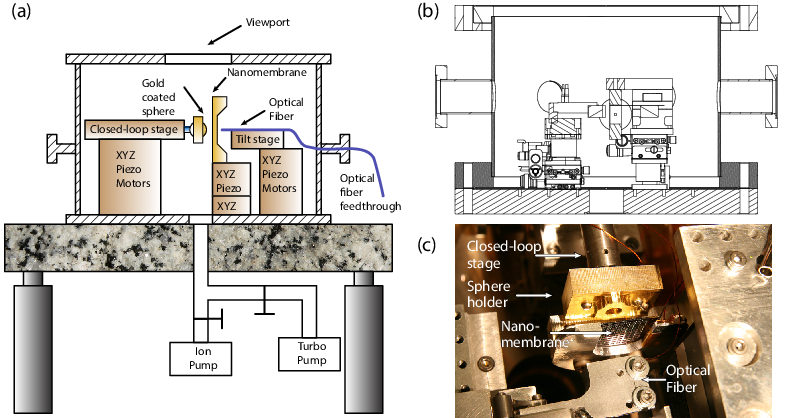
Figures 1(a) and 1(b) show a schematic illustration of the Casimir probe setup which is installed in a high vacuum chamber of . To minimize the environmental impact, the chamber is placed on top of a granite table () with pneumatic vibration isolation. Further, a wood triangle of in thickness is inserted between the vacuum chamber and the granite table to achieve optimum damping of environmental vibrations. A turbo pump system is used to pre-pump the vacuum chamber. When the chamber pressure is below , an ion pump is turned on and the turbo pump is switched off and detached from the vacuum system in order to remove the pump induced vibrations. The fiber feedthrough is constructed by modifying a Swagelok connector fitted with a teflon ferrule[12]. All electrical feedthroughs are made ultra-high vacuum (UHV) compatible by Accu-Glass Products, Inc. We finally leak-test the vacuum system with a helium leak detector, and the leaking rate is below .
The positioning system inside the vacuum chamber consists of 13 motorized stages. The sphere, the nanomembrane, and the fiber are separately mounted on three specifically designed holders, each of which is positioned by an XYZ stage controlled by picomotors[13] (See Fig. 1(a)). An additional 3-axis piezoelectrically actuated stage[14] is mounted on the nanomembrane stage to achieve sample scanning and to fine adjust fiber-to-membrane distances. The alignment of the fiber against nanomembrane is adjusted by a manual tip-tilt stage. The sphere is brought to approach the nanomenbrane by a preloaded closed-loop piezo actuator with sub-nanometer resolution ()[15]. All the stages are made vacuum compatible and carefully cleaned before installation. The movement of the stages can be carefully monitored using a telescope through the viewport at the top of the vacuum chamber. During the measurements the viewport is fully covered with metal foil to avoid ambient light which is found to introduce noise in the measurements.
II.2 Preparation of the spherical plate
Figure 2 shows the spherical plate and its holder. The sphere is prepared by coating a fused silica with of gold using of titanium as adhesion layer using an electron beam physical vapor deposition. The sphere[16] has a radius . The holder of the sphere is machined in aluminium and sputtered with gold to reduce the contact potential between the sphere and the holder. To ensure good electrical contact between the sphere and the holder a polytetrafluoroethylene (PTFE) stub is used to press the sphere against the holder, as shown in Fig. 2(b). The PTFE piece is also used to electrically isolate the sphere from the closed-loop piezo actuator and the vacuum chamber. Static charge might accumulate on the PTFE surface. But this is not a concern since the PTFE piece is fully electrically shielded from the measurement surface.

II.3 Nanomembrane fabrication
In the sphere-plane configuration, the planar plate used here is a nanomembrane fabricated from tensile-stressed silicon nitride which also serves as the force transducer. Membrane resonators made of tensile-stressed silicon nitride are known to exhibit very high mechanical Q (in the order of at room temperature)[17, 18]. The Q can be as high as even after metallization[19], which is expected to introduce extra material loss and clamping loss. From a transducer point of view, high Q implies low thermomechanical noise and so high force sensitivity. Here, we make use of this advantageous property of the high Q nanomembrane to achieve precision measurement of Casimir force.
Fabrication process of the nanomembrane is described as follows. We start with a thick, (100)-oriented, double side polished silicon wafer (doped p-type with resistivity quoted to be 10 - 20 cm). A layer of 330 nm silicon nitride is grown on both sides of the wafer by low pressure chemical vapor deposition (LPCVD). The silicon nitride SixNy used here is not stoichiometric but has a silicon-to-nitrogen ratio larger than . When deposited on a silicon substrate, the film has a built-in tensile stress of 450 MPa, which is relatively lower than that of a stoichiomeric silicon nitride. A layer of photoresist (Shipley S1813) was spun on both sides of the wafer. The photoresist on the front side serves as a protective layer. Square openings were defined in the photoresist on the backside of the wafer using photolithography and the silicon nitride layer was etched by reactive ion etching (RIE) with a mixture of CHF3 and O2 gases. After stripping off the photoresist, an anisotropic wet etch of potassium hydroxide (KOH) solution (30%, 85 ∘C for 7 hours) was used to etch through the Si substrate. During the KOH etching process a ProTEK-B3 (Brewer Science) coating was used to protect the silicon nitride layer on the top side of the wafer in order to ensure the high quality of the membrane and increase the yield. After the KOH etch, the coating was removed in a bath of N-Methyl-2-pyrrolidone (NMP) at 80 ∘C and a subsequent O2 plasma ashing. Finally of titanium and of gold were evaporated on top of the membrane, at a rate of 1 Å/s. Fig. 3(f) shows the typical optical image of a gold coated nanomembrane. Due to the net tensile stress in the film, the sample remains flat across the whole nanomembrane surface with RMS roughness of (measured by AFM). Figure 3 summarizes the nanomembrane fabrication process.

II.4 Fiber interferometer and its calibration
We first describe the fiber interferometer employed to measure the resonance of the nanomembrane. The fiber is cleaved after it has been introduced into the chamber to produce a clean cleaved surface as shown in Fig. 4(a). Figure 4(b) displays the schematic of the fiber measurement scheme. A diode laser[20] () with very low frequency noise is used as a light source. The output power of the laser is stabilized with a current and temperature controller[21] and is set to (operating current ) which corresponds to the setpoint with the lowest frequency noise. Then the light is attenuated to and sent to the nanomembrane through a circulator[22]. The light reflected from the nanomembrane returns to the circulator and is collected with a photodetector.

When the distance between the fiber and the nanomembrane is changed an interference pattern is obtained (see Fig. 5). In order to improve the extinction, the fiber axis is fine adjusted by a tip-tilt stage (see Fig. 4(b)). The maximum extinction is obtained when the fiber is perpendicular to the surface of the nanomembrane. We record the photodetector signal as the nanomembrane position is varied. The maximum sensitivity is obtained where the slope is maximal in the interference pattern (see Fig. 5), at which point a small change in distance results in a change of photodetector signal , which is related to a change by
| (1) |
where is the peak-to-peak voltage of the interference pattern and the wavelength of the laser.

II.5 Coarse approach betwen the fiber and the nanomembrane
When the fiber is brought to approach the nanomembrane, the distance between the fiber and the nanomembrane is measured in real time to avoid physical contact and breaking of the nanomembrane. We achieve this at each distance by sweeping the wavelength using a tunable laser[23], and recording the maxima and minima of the interferometer signal. The distance is given by
| (2) |
where is the distance between the fiber and the nanomembrane, the number of peaks in the interference pattern in the wavelength regime, the starting wavelength and the final wavelength.
In order to collect the maximum amount of light reflected by the nanomembrane the fiber has to be very close to the nanomembrane because of the relative small numerical aperture of the single mode fiber. With fiber-membrane distance monitored in real time, the fiber is brought to the closest yet safe distance from the nanomembrane by operating the picomotors. During the approach the fiber is aligned several times with a tip-tilt stage[24] (see Fig. 4(b)). When the fiber is aligned the extinction of the interference pattern is maximized. By doing this, we improve the sensitivity of the interferometer and are able to approach to a very close distance. We then move the nanocube Z stage to fine tune the fiber-membrane distance so that maximum sensitivity is achieved in our fiber interferometer.
II.6 Setup stability evaluation
In order to minimize the mechanical drift of the fiber interferometer and the apparatus the room temperature is kept at . The big mass of the vacuum system further filters out the variations of the temperature of the room. We characterize the stability of the setup by monitoring the interferometer signal overnight. As shown in Fig. 6 the measured drift of the fiber-to-membrane distance is about which is probably due to the thermal expansion of the apparatus and stages. As explained in the next section one single measurement (a parabola fitting) takes about which corresponds to a drift of which is negligible when compared with other sources of error, such as the determination of the distance and the measurement of the resonance frequency of the nanomembrane.

II.7 Nanomembrane characterization
We measured the frequency response of the SiN gold coated nanomembranes and studied how the quality factor is modified when they are covered with gold. The nanomembrane is excited with an oscillating voltage which is applied to the piezo actuator and the response is measured with the fiber interferometer. The amplitude-frequency response of the nano-membrane was obtained by measuring the oscillation amplitude of the nano-membrane and sweeping the driving frequency excitation. The frequency response was measured in a set of samples where the amount of surface covered by gold changes (see Figs. 7(a) and 7(b)). It goes from fully covered by a layer of of gold to not covered at all. Fig. 7(c) shows the response curve of a nanomembrane which is not covered by gold and Fig. 7(d) shows the response curve of a nanomembrane which is fully covered by a layer of of gold. As we increase the amount of surface coverage the resonance frequency decreases because the total mass of the nanomembrane increases, this is shown in Fig. 7(e). When the nanomembrane is covered with some gold the quality factor is reduced, but we have not observed a deterministic trend of the quality factor with regards to the gold coverage as shown in Fig. 7(f). Hence we choose fully covered membrane in our following measurements.

II.8 Frequency drift and resolution
The frequency of the nanomembrane is tracked using a phase-locked loop (PLL) scheme. The output of the photodiode is compared with a reference signal using a lock-in amplifier that has a built-in PLL capability[25]. We use the frequency shift of the nanomembrane to calculate the Casimir and the electrostatic forces (see section III.1). The temperature drift of the nano-membrane can also shift the resonance frequency. As mentioned before the temperature of the room is stabilized to and also the big mass of the chamber stabilizes the temperature of the nanomembrane. The ambient light can also substantially heat up the nanomembrane and shift the resonance frequency, therefore all the viewports of the chamber are blinded. When ambient light is allowed to enter into the chamber the frequency drift is about , and when the viewports are blinded the frequency drift is (see Fig. 8(a)). The frequency drift is constant during a period of time much longer than a typical measurement, which is shorter than one second. Before any measurement the frequency drift is calibrated and the measurements are corrected according to this calibration. By optimizing all the relevant conditions, we achieve a frequency resolution of which allows to measure a force gradient of (see Fig. 8(b)). As shown in the Allan deviation the drift becomes relevant above a measurement time of which is smaller than the measurement time of one parabola.

III Measurement scheme
III.1 Principle
To measure the Casimir force we use the resonance frequency of the nanomembrane as a transducer which is very sensitive to the force gradient. When the nanomembrane approaches the sphere, it experiences a force which has contributions from the Casimir Force as well as the electrostatic force. This force is distributed over the whole nanomembrane and the force per unit of surface can be expressed as , where represents the magnitude of the force and the normalized spatial distribution of the force. Now if we consider the first 3 terms of the Taylor expansion of the external force about the distance , the equation of motion of the nanomembrane becomes
where is the fundamental angular frequency of the nanomembrane, the angular driving frequency, is the damping coefficient, the stiffness of the nanomembrane and the eigenvector of the first eigenmode. The product accounts for the overlap between the force and the eigenmode. We can then define the effective stiffness as:
| (4) |
In the case of the first eigenmode the overlap between the force and the eigenmode will be maximum when the sphere is centered on top of the nanomembrane, and the stiffness will be minimum from the point of view of the external force.
The amplitude of motion of the resonator is set to be in the linear regime but there is some contribution from high order derivatives of the external force. If we consider a small non-linearity the resonance frequency can be approximated by
| (5) | |||||
where is the apparent force and the RMS amplitude of motion of the resonator. The contribution of the third derivative of the force to the frequency shift can be considered as a correction and is equivalent to the corrections for the roughness and the fluctuations in plate separation that have been considered in previous experiments[26, 3].
III.2 Measurement procedure
When a difference of voltage is applied between the sphere and the nanomembrane an electrostatic force appears and is given by
| (6) |
where is the vacuum permittivity, the radius of the sphere, the absolute distance between the sphere and the nanomembrane, the relative distance which is set with the closed-loop piezo actuator and the residual contact potential.
As shown in Figs. 9(a) and 9(b), the contribution of the electrostatic force to the frequency shift can be fitted to a parabola characterized by a curvature . Therefore at each distance between the sphere and the nanomembrane it can be found that the frequency shift is given by[27]
| (7) | |||||
In this equation accounts for the electrostatic force that can be nulled by applying a voltage between the sphere and the nanomembrane. Note that is not necessarily constant with the relative position between the membrane and the sphere and it has been shown that such a variation of can cause an additional electrostatic force[10, 28]. accounts for the Casimir force and the electrostatic force that can not be cancelled. To calculate the magnitudes , and the distance between the sphere and the nanomembrane is fixed and three different voltages , and are applied between the sphere and the nanomembrane. For each voltage a frequency shift is measured: , and . With these measurements we can calculate the desired magnitudes and their dependence with the distance .
| (9) | |||||
| (10) |

In order to compensate for the drift in frequency of the nanomembrane, the measured quantities , and have been corrected. By fitting to the expected model[29] the quantities and can be obtained. With these quantities we can have an absolute calibration of the distance. Fig. 9(c) shows a typical measurement of and the fit with of . The fit gives as a result an effective mass of . The expected theoretical effective mass for this particular nanomembrane is . In the measurement of Fig. 9(c) the nanomembrane appears to be heavier because in this measurement the sphere is not centered on top of the nanomembrane.
is voltage that has to be applied to minimize the electrostatic contribution to the force. This voltage may not be constant with the distance between the sphere and the nanomembrane[28, 30]. The quantity has contributions from the Casimir force but also from the residual electrostatic force that can not be completely canceled even by setting the external voltage to . This force has the origin in the interplay between the surface patches and the curvature of the sphere.
| (11) |
where is the Casimir force and is the residual electrostatic force[28, 10]. To reduce the error introduced by the drift of the frequency in , two parabola measurements are done, one at a very far distance and another one at the target distance . This gives as a result and respectively. is equal to the subtraction between these two frequencies. This procedure is repeated several times to improve the signal to noise ratio of at . The value is the average of all the measured at that particular distance. Fig. 9(d) shows a typical measurement of , and the inset shows the contact potential vs the distance with the sphere. Note that Fig. 9c and Fig. 9d are based on different sets of data. The calibration curve of Fig. 9c is obtained using the displacement data of the closed loop piezo actuator. To be insensitive to the drift of the system this data has been taken quite fast. Once the system is calibrated we can measure and by doing repetitions of the same measurement in order to improve the accuracy (see Fig. 9d). In this case the displacement data of the piezo actuator is discarded and the distance is calculated using the measured . This method is very accurate and insensitive to the mechanical drift.
III.3 Surface potential measurements
Scanning Kelvin probe principle is a very powerful noninvasive technique[31, 32, 33] that allows to measure the surface contact potential between a conducting tip and a sample. The surface contact potential is related to the difference of the work function between the sphere and the nanomembrane
| (12) |
where is the elementary charge and and are the work functions of the tip and the sample respectively. The work function and as a consequence the surface contact potential can vary along the surface due to oxides films or adsorbed chemicals on the surface and produce the patch potentials[28, 10]. Our setup allows for in-situ measurements of the surface potentials on the nanomembrane. The sphere can be moved parallel to the nanomembrane using the XYZ Piezo System in order to image the surface potential at a fix distance between the sphere and the nano-membrane. The movement of the axes and from the nanocube is not completely parallel to the sphere, therefore when we move the nanomembrane using the axis and the distance between the sphere and the nanomembrane changes. In order to measure the contact potential at a fix distance , a calibration curve is taken at each point . Then using the calibration curve the sphere is placed at a distance from the nanomembrane and the contact potential is measured. Fig. 10(b) shows the measurement of the contact potential of a sample where the variations of the contact potentials are large. These contact potentials play an an important role in the precise measurement of the Casimir force[10]. The spatial variations of the contact potential create an electric field between the sphere and the nanomembrane which originates a residual electrostatic force that cannot be completely canceled by applying a a voltage between the sphere and the nanomembrane.

The effective stiffness also depends on the relative position between the sphere and the nano-membrane. More specifically it depends on the overlap between the mechanical mode of the nano-membrane and the distribution of the electrostatic force (see equation (4)). The effective stiffness is minimum, when the overlap between the mechanical eigenmode and the electrostatic force is maximum, that is when the sphere is centered over the nanomembrane. When the sphere gets farther from the center of the nanomembrane, the overlap between the eigenmode and the electrostatic force becomes smaller and the effective stiffness betcomes bigger. The spatial dependence of the effective stiffness can be used to center the sphere over the top of the nanomembrane. Figure 10(a) shows the contour mapping of the measured stiffness at the center of a nano-membrane.
IV Conclusion
We have designed a Casimir force probe that allows in situ measurements of the contact potential and bridges the measurement of the Casimir force at microscale and macroscale. The Casimir force measurement is based on a sphere-plane geometry where the planar plate is a high Q silicon nitride nanomembrane coated with gold. The probe can measure a force gradient down to . We have also studied the dependence of the quality factor of the nanomembrane with the amount of coated gold and we have observed that the SiN nanomembranes coated with gold can retain a reasonably high quality factor. In situ scanned Kevin probe allows direct assessment of contact potentials and their distributions, which are found to contribute significantly to the measured position dependence forces in most samples we have tested.
References
- [1] M. Sparnaay, “Measurements of attractive forces between flat plates,” Physica 24, 751 – 764 (1958).
- [2] S. K. Lamoreaux, “Demonstration of the casimir force in the 0.6 to range,” Phys. Rev. Lett. 78, 5–8 (1997).
- [3] A. O. Sushkov, W. J. Kim, D. A. R. Dalvit, and S. K. Lamoreaux, “Observation of the thermal casimir force,” Nat Phys 7, 230–233 (2011).
- [4] U. Mohideen and A. Roy, “Precision measurement of the casimir force from 0.1 to ,” Phys. Rev. Lett. 81, 4549–4552 (1998).
- [5] J. N. Munday, F. Capasso, and V. A. Parsegian, “Measured long-range repulsive casimir-lifshitz forces,” Nature 457, 170–173 (2009).
- [6] E. Buks and M. L. Roukes, “Metastability and the casimir effect in micromechanical systems,” Europhys. Lett. 54, 220–226 (2001).
- [7] H. B. Chan, V. A. Aksyuk, R. N. Kleiman, D. J. Bishop, and F. Capasso, “Quantum mechanical actuation of microelectromechanical systems by the casimir force,” Science 291, 1941–1944 (2001a).
- [8] H. B. Chan, V. A. Aksyuk, R. N. Kleiman, D. J. Bishop, and F. Capasso, “Nonlinear micromechanical casimir oscillator,” Phys. Rev. Lett. 87, 211801 (2001b).
- [9] G. Bressi, G. Carugno, R. Onofrio, and G. Ruoso, “Measurement of the casimir force between parallel metallic surfaces,” Phys. Rev. Lett. 88, 041804 (2002).
- [10] D. Garcia-Sanchez, K. Y. Fong, H. Bhaskaran, S. Lamoreaux, and H. X. Tang, “Casimir force and In Situ surface potential measurements on nanomembranes,” Phys. Rev. Lett. 109, 027202 (2012).
- [11] W. H. P. Pernice, M. Li, D. Garcia-Sanchez, and H. X. Tang, “Analysis of short range forces in opto-mechanical devices with a nanogap,” Opt. Express 18, 12615–12621 (2010).
- [12] E. R. Abraham and E. A. Cornell, “Teflon feedthrough for coupling optical fibers into ultrahigh vacuum systems,” Appl. Opt. 37, 1762–1763 (1998).
- [13] Ultra-High Vacuum Picomotor Actuator. Model: 8301-UHV.
- [14] p-611.3 NanoCube XYZ Piezo Stage.
- [15] p-841.20 Preloaded Closed-Loop Piezo Actuator. PI (Physik Instrumente).
- [16] The sphere is a fused silica ball lens from Edmund Optics with ref. NT67-388.
- [17] J. D. Thompson, B. M. Zwickl, A. M. Jayich, F. Marquardt, S. M. Girvin, and J. G. E. Harris, “Strong dispersive coupling of a high-finesse cavity to a micromechanical membrane,” Nature 452, 72 (2008).
- [18] I. Wilson-Rae, R. A. Barton, S. S. Verbridge, D. R. Southworth, B. Ilic, H. G. Craighead, and J. M. Parpia, “High- nanomechanics via destructive interference of elastic waves,” Phys. Rev. Lett. 106, 047205 (2011).
- [19] P.-L. Yu, T. P. Purdy, and C. A. Regal, “Control of material damping in high- membrane microresonators,” Phys. Rev. Lett. 108, 083603 (2012).
- [20] 1310nm laser from Applied Optoelectronics. ref: DBF-2287-BF-10-A4-FA-444.
- [21] Laser Diode Controllers from ILX Lightwave. Model: LDC-3744B.
- [22] fOC-12N-111-9/125-SSS-1310-55-3A3A3A-1-1, Oz Optics.
- [23] Santec ECL-210 Tunable Laser Diode.
- [24] Rotational stage from NewPort. Ref:9873-K.
- [25] HF2 lock-in amplifier from Zurich Instruments.
- [26] S. K. Lamoreaux, “Reanalysis of casimir force measurements in the 0.6-to-6um range,” Phys. Rev. A 82, 024102 (2010).
- [27] M. Brown-Hayes, D. A. R. Dalvit, F. D. Mazzitelli, W. J. Kim, and R. Onofrio, “Towards a precision measurement of the casimir force in a cylinder-plane geometry,” Phys. Rev. A 72, 052102 (2005).
- [28] W. J. Kim, A. O. Sushkov, D. A. R. Dalvit, and S. K. Lamoreaux, “Surface contact potential patches and casimir force measurements,” Phys. Rev. A 81, 022505 (2010).
- [29] W. J. Kim, A. O. Sushkov, D. A. R. Dalvit, and S. K. Lamoreaux, “Measurement of the short-range attractive force between ge plates using a torsion balance,” Phys. Rev. Lett. 103, 060401 (2009).
- [30] S. Lamoreaux, “Electrostatic background forces due to varying contact potentials in casimir experiments,” arXiv:0808.0885 (2008).
- [31] N. A. Robertson, J. R. Blackwood, S. Buchman, R. L. Byer, J. Camp, D. Gill, J. Hanson, S. Williams, and P. Zhou, “Kelvin probe measurements: investigations of the patch effect with applications to st-7 and lisa,” Classical and Quantum Gravity 23, 2665 (2006).
- [32] M. Nonnenmacher, M. P. O’Boyle, and H. K. Wickramasinghe, “Kelvin probe force microscopy,” Applied Physics Letters 58, 2921–2923 (1991).
- [33] A. Kikukawa, S. Hosaka, and R. Imura, “Silicon pn junction imaging and characterizations using sensitivity enhanced kelvin probe force microscopy,” Applied Physics Letters 66, 3510–3512 (1995).