Ferroelectric-Gated Terahertz Plasmonics on Graphene
Abstract
Inspired by recent advancement of low-power ferroelectic-gated memories and transistors, we propose a design of ferroelectic-gated nanoplasmonic devices based on graphene sheets clamped in ferroelectric crystals. We show that the two-dimensional plasmons in graphene strongly couple with the phonon-polaritons in ferroelectrics at terahertz frequencies, leading to characteristic modal wavelength of the order of 100–200 nm at only 3–4 THz. By patterning the ferroelectrics into different domains, one can produce compact on-chip plasmonic waveguides, which exhibit negligible crosstalk even at 50 nm separation distance. Harnessing the memory effect of ferroelectrics, low-power electro-optical switching can be achieved on these plasmonic waveguides.
The emergence of graphene research in the recent years has triggered a significant interest in two-dimensional plasmonics.[1, 2, 3, 4, 5, 6, 7, 8, 9] The transport behaviors of graphene reveal extremely low ohmic loss and nearly perfect electron-hole symmetry.[10, 11, 12, 13, 14] The charge-carrier density (or the Fermi level) can be conveniently adjusted via chemical doping and electrostatic gating, which give rise to tunable plasmonic oscillations in the terahertz frequency regime.[2, 3] In combination with its remarkable character of single-atom thickness and the ability of subwavelength light confinement, graphene has become a promising platform for the new-generation nanoplasmonic devices.[4, 6] So far the most widely studied graphene plasmonic structures are fabricated on silicon dioxide (SiO2) substrates or suspended in air,[15, 16, 17] where the SiO2 and air serve as the dielectric claddings for the creation of surface plasmon-polaritons (SPPs).[18] In contrast with conventional dielectrics, ferroelectrics such as lithium niobate (LiNbO3) and lithium tantalate (LiTaO3) bear giant permittivity and birefringence at terahertz frequencies.[19, 20] This peculiarity is associated with the coexistence of terahertz phonon-polariton modes[21, 22] and static macroscopic polarization.[23, 24, 25] It is thus of particular interest to investigate whether the unique properties of ferroelectrics can be integrated into nanoplasmonics,[26, 27, 28] and especially, display a strong coupling with graphene plasmonics in the same terahertz range.

In this paper, we propose a design of ferroelectic-gated graphene plasmonic devices operating at THz frequencies. Figure 1 illustrates the building blocks, while more complex structures can be made based on the same idea. This type of architecture has at least two appealing features that are not present in the common dielectric-graphene-dielectric architecture, and may bring fresh insight into the design of (classical or quantum) optical circuits. The first feature originates from the extremely large permittivity and comparatively high -value near the optical-phonon resonances of ferroelectrics at terahertz frequencies.[19] When the two-dimensional plasmons in graphene become coupled with the phonon-polaritons in ferroelectrics by exchanging photons across their interfaces, they form the so-called surface plasmon-phonon-polaritons (SPPPs) and lead to around 100 nm modal wavelength, even if the driving frequency remains at a few THz. These subwavelength modes are fundamentally supported by the atomic-level oscillations of ferroelectric ions and are limited by the dissipation through anharmonic phonon processes.[21, 29, 30] The second feature lies in the large macroscopic polarization in ferroelectrics of the order of C cm-2, corresponding to a large surface bound-charge density of the order of cm-2.[24, 23, 22] The parallel- and antiparallel-poling configurations can induce drastically different free-charge densities on graphene, which effectively switch off and on the Fermi energy by about eV. These features may be employed for constructing nanoplasmonic elements (waveguides, resonators, antennae, etc.) through the electrostatic gating of ferroelectrics.[31, 32] Thanks to the memory effect of ferroelectrics, an intended design can sustain itself without a need of constant input bias, and can be conveniently refreshed in a low-power manner, similar to those operations in the ferroelectric random-access memories (FeRAM) and ferroelectric field-effect transistors (FeFET).[24, 23, 33, 34]
Let us first study the eigen-modes on an infinite ferroelectric-graphene-ferroelectric structure. Suppose the materials being stacked along the -axis, and infinitely extended in the -plane, matching the same coordinate system indicated in Fig. 1. The graphene sheet is situated at with a zero thickness yet a nonzero two-dimensional conductivity .[1, 4, 6] The two ferroelectric crystals occupy the semi-infinite regions and , respectively. We assume the macroscopic polarizations of the ferroelectrics to be aligned with either or direction, so the optical axes of the crystals always coincide with the -axis.[22, 25] The static polarity mainly affects the electron density on graphene but has no appreciable impact on the optical properties in bulk crystals.[24, 23, 33, 34] The eigen-solutions of the entire structure can be labeled by frequency and in-plane wavenumbers and across all the regions. Within each region, the electric field and the magnetic field are linear combinations of plane waves associated with an out-of-plane wavenumber . For surface-wave solutions, is an imaginary number. Due to anisotropy, we may define the ordinary and extraordinary two evanescent wavenumbers with respect to the optical -axis, , , respectively. and are the ordinary and extraordinary permittivities of the ferroelectrics.[19, 20] After some boundary treatment, we shall find the dispersion relation (in the cgs units),
| (1) |
which is an anisotropic generalization to the dispersion relation in dielectric-graphene-dielectric structures.[1]
In graphene plasmonics, the Fermi energy measured from the Dirac point usually ranges from about eV to eV, equivalent to an electron or hole concentration varying from cm-2 to cm-2 according to the relation , where is the Fermi velocity taken as cm s-1.[10, 11, 12, 13, 14] For the experiments below 10 THz, the simple Drude formula can quite accurately describe the graphene conductivity (in the cgs units),[1, 2, 4, 5, 6] , where is the relaxation rate. For an ultra-pure sample, the usual mobility limitation comes from the electron scatterings with the thermally-excited acoustic phonons in graphene and the remote optical phonons from SiO2.[11, 12, 15, 13, 14] According to the literature, we estimate the mobility for our structure to be of the order of cm2 V-1s-1 at room temperature ( K), and cm2 V-1 s-1 at low temperature ( K).[35] The relaxation rate can be calculated from mobility via .[13, 14]
We choose LiNbO3 as an example of ferroelectric materials. It is especially convenient for low-THz experiments, because the extraordinarily polarized THz waves can be triggered by 800 nm femtosecond laser pulses via nonlinear optical response inside LiNbO3.[19, 36] According to the Raman scattering data,[22, 37, 38, 39] LiNbO3 has two fundamental transverse optical-phonon frequencies and , corresponding to the ordinary and extraordinary waves, respectively. The main behaviors of the permittivities and in the 0.1–10 THz frequency range can be fitted by the Lorentz model,[19, 21] , , where , , , are the high-frequency and low-frequency limits of and , and are the relaxation rates associated with anharmonic optical-phonon decaying. We adopt their room-temperature ( K) values from Ref. [19], and set the low-temperature ( K) and to be about one third of their room-temperature values according to Ref. [37, 38, 39] and undergo near divergence and sign change around and , signifying the high- resonant coupling between photons and optical phonons. They turn back to positive at the longitudinal optical-phonon frequencies THz and THz in this model.[19, 21]
For the plane-wave study, we set and choose as the progressive wavenumber, which can be explicitly solved as
| (2) |
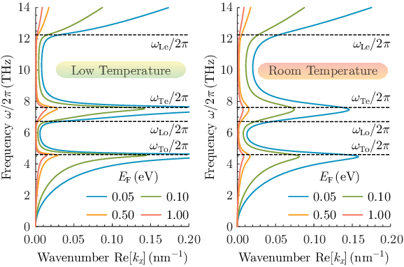
The modal wavelength , the attenuation length , and the confining length can be defined accordingly. For a Fermi energy between 0.05–1.0 eV, and driving frequency in the range of 1–10 THz, the dispersion relation is primarily controlled by the second term of Eq. (2). The plasmon behavior is strongly affected by the optical-phonon resonances. So the combined excitations are surface plasmon-phonon-polaritons (SPPPS). Figure 2 shows the dispersion relation under different conditions. For each given , the dispersion curves mainly stay in the three allowed-bands: , , and , but weakly leak into the two forbidden-bands: and . Finite-valued relaxation rates broaden the sharp peaks around the optical-phonon resonances. For a small , the dispersion curves bend more considerably towards the optical-phonon lines and can give very large at low frequencies; for a large , the dispersion curves mostly attach to the THz light line (very close to the -axis and cannot be identified in the scale of Fig. 2). In reality, there exist other optical-phonon resonances higher than and ,[37, 38, 39] which will make the curves in Fig. 2 more kinked than as shown. But we will only focus on the frequency region close to the fundamental optical-phonon resonance THz from below. In Table 1, we list the calculated characteristic quantities at about 100 K. For low-power sensitive THz-photon manipulation, a low temperature is helpful for suppressing the thermal noise or dissipation.[13, 14, 37, 38, 39] In Table 1, one can see clearly the huge effective refractive index and ultra-short modal wavelength compared with the free-space wavelength of low-THz photons. Large dissipation occurs at frequencies above 4.0 THz. But just below it, for eV, the wavelength can indeed be squeezed to 100–200 nm while the confining length is only about 10–20 nm.
| (eV) | (THz) | (nm) | (nm) | (nm) | |
|---|---|---|---|---|---|
| 0.05 | 2.5 | 532+14i | 225 | 1386 | 27 |
| 3.0 | 694+21i | 144 | 760 | 16 | |
| 3.5 | 922+37i | 93 | 364 | 10 | |
| 4.0 | 1335+95i | 56 | 126 | 5 | |
| 4.5 | 2836+1045i | 23 | 10 | 1 | |
| 0.10 | 2.5 | 266+5.2i | 450 | 3676 | 53 |
| 3.0 | 347+8.6i | 288 | 1846 | 32 | |
| 3.5 | 461+17i | 186 | 820 | 19 | |
| 4.0 | 668+45i | 112 | 266 | 10 | |
| 4.5 | 1420+518i | 47 | 20 | 3 | |
| 0.50 | 2.5 | 53+0.8i | 2252 | 24879 | 266 |
| 3.0 | 69+1.4i | 1440 | 11133 | 162 | |
| 3.5 | 92+3.0i | 929 | 4563 | 96 | |
| 4.0 | 134+8.5i | 561 | 1397 | 49 | |
| 4.5 | 284+103i | 234 | 103 | 13 | |
| 1.00 | 2.5 | 27+0.4i | 4504 | 52058 | 532 |
| 3.0 | 35+0.7i | 2880 | 22856 | 324 | |
| 3.5 | 46+1.5i | 1858 | 9255 | 192 | |
| 4.0 | 67+4.2i | 1122 | 2812 | 97 | |
| 4.5 | 142+51i | 469 | 207 | 26 |
As an example, we now employ the large difference in the length scale of SPPPs under different Fermi energies to make low-power subwavelength waveguides. LiNbO3 is known to possess very large spontaneous polarization . In a bulk crystal under zero electric field, C cm-2,[25, 22, 40] which is equivalent to a surface bound-charge density cm-2. In a thin film of about 200 nm thick, C cm-2,[40] and the equivalent surface bound-charge density is cm-2. For our studies, we take the 200 nm thickness for each slab of LiNbO3. As shown in Fig. 1, for the parallel-poling configuration, the bound charges of opposite signs from the lower and upper slabs cancel each other, leaving an approximately zero-potential setting for the graphene sheet. Thus the charge-carrier density on graphene is solely determined by chemical doping. But for the antiparallel-poling configuration, the bound charges of the same sign from the both slabs cause a net positive or negative potential on the graphene sheet. For the 200 nm thin film clamping, the induced charge-carrier density is cm-2 which is equivalent to a nearly eV electrostatic gating based on the preceding calculation. In the numerical simulation below, we assume that a small eV is built in graphene from chemical doping, and is reserved between the parallel-poling domains, while a large eV is generated between the antiparallel-poling domains due to the ferroelectric gating. The slight difference in between the electron and hole cases is neglected because of the smallness of 0.05 eV compared with 1.0 eV. The electron-hole symmetry in graphene plays an important role here.
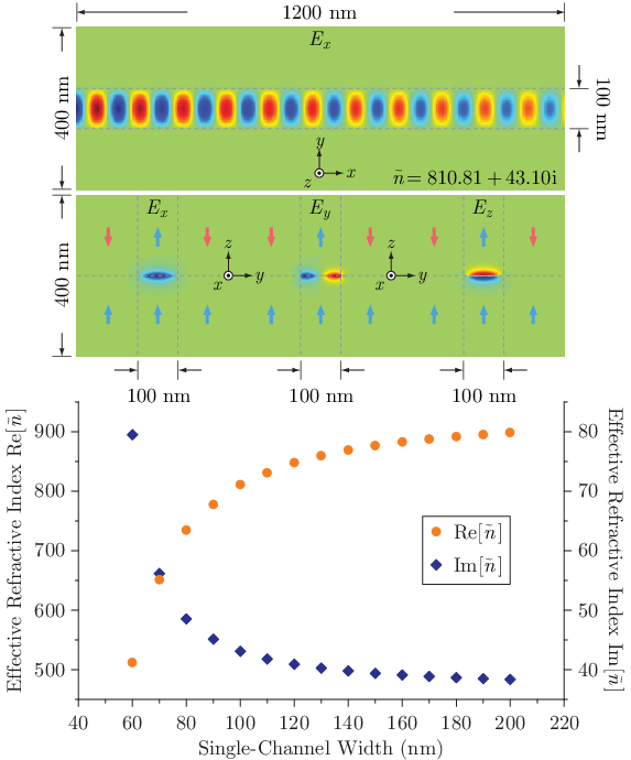
We choose the frequency 3.5 THz for all our finite-difference time-domain (FDTD) simulations. The free-space photon wavelength is 85.7 m. For the domain poling configuration shown in Fig. 3, a single eV channel is produced in between two eV barriers. As can be inferred from our previous discussion, a low- channel is more “dielectric” in the sense that it carries less charges but hosts more photons, whereas a high- channel is more “metallic” in the sense that it carries more charges but permits less photons. Thus the deep subwavelength SPPP modes preferably flow in the middle channel with very tiny penetration into the left- and right-barriers. The lower panel of Fig. 3 shows the real and imaginary parts of the effective refractive index changing with the channel width. One can see that the waveguide mode undergoes exponentially stronger attenuation and weaker subwavelength after the channel width goes down to below 100 nm, consistent with the 93 nm plane-wave modal wavelength at 3.5 THz in Table 1. We choose 100 nm to plot the profiles of each electric-field component in the upper panel of Fig. 3. For the effective refractive index in this case, the modal wavelength nm, and the attenuation length nm.
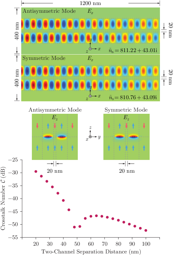
The exceptional confining quality of the prescribed ferroelectric-gated channel can be manifested by putting two such channels close to each other and see how the modes in the two channels become coupled by varying the separation distance.[17, 41, 42] We may define a dimensionless crosstalk number,
| (3) |
which estimates (in terms of dB) the number of modal (not free-space) wavelength needed, for an injected power initially in one channel to be transferred into the other and then be transferred back. In Fig. 4, we can see the simulated crosstalk number to be mostly in the range of to dB. For the plotted pattern of 20 nm separation distance, this number is still far below zero at dB. The dissipation has certainly come in at a much shorter propagation distance, so the waves cannot really travel that far.[42] But this number still shows the extreme confining quality in these ferroelectric-graphene waveguides compared with conventional dielectric and plasmonic waveguides. For example, silicon waveguides with similar dimensions at infrared frequencies have a crosstalk number of the order of dB in accordance with our definition.[41] Ba0.5Sr0.5TiO3-metal inter-layer plasmonic waveguides at visible-light frequencies can have a crosstalk number of the order of dB, but must take a much larger separation distance.[26] One may notice a singular drop at about 50 nm on the calculated curve in the lower panel of Fig. 4. Based on an analysis to the dipole-dipole coupling in this particular system, we find it to be due to a competition between the relative magnitudes of field components. A large field tends to make the symmetric mode have a higher refractive index, while a large or field tends to make the antisymmetric mode have a higher refractive index. The 50 nm separation distance between two 100 nm wide waveguides happens to be the turning point, where . A more thorough study on this phenomena will be performed.
We acknowledge the financial support by NSF (ECCS Award No. 1028568) and the AFOSR MURI (Award No. FA9550-12-1-0488).
References
- [1] M. Jablan, H. Buljan, and M. Soljačić, Phys. Rev. B 80, 245435 (2009).
- [2] J. Long, B. Geng, J. Horng, C. Girit, M. Martin, Z. Hao, H. A. Bechtel, X. Liang, A. Zettl, Y. R. Shen, and F. Wang, Nature Nanotechnology 6, 630 (2011).
- [3] S. Ryu, J. Maultzsch, M. Y. Han, P. Kim, and L. E. Brus, ACS Nano 5, 4123 (2011).
- [4] F. H. L. Koppens, D. E. Chang, and F. J. García de Abajo, Nano Lett. 11, 3370 (2011).
- [5] A. R. Davoyan, V. V. Popov, and S. A. Nikitov, Phys. Rev. Lett. 108, 127401 (2012).
- [6] Q. Bao and K. P. Loh, ACS Nano 6, 3677 (2012).
- [7] A. Vakil and N. Engheta, Science 332, 1291 (2011).
- [8] J. Chen, M. Badioli, P. Alonso-González, S. Thongrattanasiri, F. Huth, J. Osmond, M. Spasenović, A. Centeno, A. Pesquera, P. Godignon, A. Z. Elorza, N. Camara, F. Javier García de Abajo, R. Hillenbrand, and F. H. L. Koppens, Nature 487, 77 (2012).
- [9] Z. Fei, A. S. Rodin, G. O. Andreev, W. Bao, A. S. McLeod, M. Wagner, L. M. Zhang, Z. Zhao, M. Thiemens, G. Dominguez, M. M. Fogler, A. H. C. Neto, C. N. Lau, F. Keilmann, and D. N. Basov, Nature 487, 82 (2012).
- [10] A. K. Geim and K. S. Novoselov, Nature Materials 6, 183 (2007).
- [11] K. I. Bolotin, K. J. Sikes, J. Hone, H. L. Stormer, and P. Kim, Phys. Rev. Lett. 101, 096802 (2008).
- [12] S. V. Morozov, K. S. Novoselov, M. I. Katsnelson, F. Schedin, D. C. Elias, J. A. Jaszczak, and A. K. Geim, Phys. Rev. Lett. 100, 016602 (2008).
- [13] N. M. R. Peres, Rev. Mod. Phys. 82, 2673 (2010).
- [14] S. Das Sarma, S. Adam, E. H. Hwang, and E. Rossi, Rev. Mod. Phys. 83, 407 (2011).
- [15] J. H. Chen, C. Jang, S. Xiao, M. Ishigami, and M. S. Fuhrer, Nature Nanotechnology 3, 206 (2008).
- [16] A. Y. Nikitin, F. Guinea, F. J. García-Vidal, and L. Martín-Moreno, Phys. Rev. B 84, 161407 (2011).
- [17] J. Christensen, A. Manjavacas, S. Thongrattanasiri, F. H. L. Koppens, and F. J. García de Abajo, ACS Nano 6, 431 (2012).
- [18] E. N. Economou, Phys. Rev. 182, 539 (1969).
- [19] T. Feurer, N. S. Stoyanov, D. W. Ward, J. C. Vaughan, E. R. Statz, and K. A. Nelson, Annu. Rev. Mater. Res. 37, 317 (2007).
- [20] Y. M. Sun, Z. L. Mao, B. H. Hou, G. Q. Liu, and L. Wang, Chin. Phys. Lett. 24, 414 (2007).
- [21] N. W. Ashcroft and N. D. Mermin, Solid State Physics (Brooks Cole, 1976).
- [22] V. Marek, First-principles study of ferroelectric oxides, Ph.D. thesis, Université de Liège (2003).
- [23] N. Setter, D. Damjanovic, L. Eng, G. Fox, S. Gevorgian, S. Hong, A. Kingon, H. Kohlstedt, N. Y. Park, G. B. Stephenson, I. Stolitchnov, A. K. Taganstev, D. V. Taylor, T. Yamada, and S. Streiffer, J. Appl. Phys. 100, 051606 (2006).
- [24] M. Dawber, K. M. Rabe, and J. F. Scott, Rev. Mod. Phys. 77, 1083 (2005).
- [25] S. Sanna and W. G. Schmidt, Phys. Rev. B 81, 214116 (2010).
- [26] S. W. Liu and M. Xiao, Appl. Phys. Lett. 88, 143512 (2006).
- [27] J. E. Spanier, A. M. Kolpak, J. J. Urban, I. Grinberg, L. Ouyang, W. S. Yun, A. M. Rappe, and H. Park, Nano Lett. 6, 735 (2006).
- [28] M. J. Dicken, L. A. Sweatlock, D. Pacifici, H. J. Lezec, K. Bhattacharya, and H. A. Atwater, Nano Lett. 8, 4048 (2008).
- [29] A. Harhira, L. Guilbert, P. Bourson, and H. Rinnert, Phys. Status Solidi C 4, 926 (2007).
- [30] V. H. Arakelian and N. M. Hovsepian, Phys. Status Solidi B 164, 147 (1991).
- [31] A. Haussmann, P. Milde, C. Erler, and L. M. Eng, Nano Lett. 9, 763 (2009).
- [32] D. Li and D. A. Bonnell, Annu. Rev. Mater. Res. 38, 351 (2008).
- [33] Y. Zheng, G.-X. Ni, C.-T. Toh, M.-G. Zeng, S.-T. Chen, K. Yao, and B. Ozyilmaz, Appl. Phys. Lett. 94, 163505 (2009).
- [34] E. B. Song, B. Lian, S. M. Kim, S. Lee, T.-K. Chung, M. Wang, C. Zeng, G. Xu, K. Wong, Y. Zhou, H. I. Rasool, D. H. Seo, C. H.-J, J. Heo, S. Seo, and K. L. Wang, Appl. Phys. Lett. 99, 042109 (2011).
- [35] X. Hong, A. Posadas, K. Zou, C. H. Ahn, and J. Zhu, Phys. Rev. Lett. 102, 136808 (2009).
- [36] J. Hebling, K.-L. Yeh, M. C. Hoffmann, and K. A. Nelson, IEEE Journal of Selected Topics in Quantum Electronics 14, 345 (2008).
- [37] S. V. Ivanova, V. S. Gorelik, and B. A. Strukov, Ferroelectrics 21, 563 (1978).
- [38] P. Capek, G. Stone, V. Dierolf, C. Althouse, and V. Gopolan, Phys. Status Solidi C 4, 830 (2007).
- [39] M. L. Hua, C. T. Chia, J. Y. Changa, W. S. Tse, and J. T. Yu, Mater. Chem. Phys. 78, 358 (2002).
- [40] V. Joshi, D. Roy, and M. L. Mecartney, Appl. Phys. Lett. 63, 1331 (1993).
- [41] C. Yeh and F. Shimabukuro, The Essence of Dielectric Waveguides (Springer, 2008).
- [42] G. Veronis and S. Fan, Opt. Express 16, 2129 (2008).