Exact solution for square-wave grating covered with graphene: Surface plasmon-polaritons in the THz range
Abstract
We provide an analytical solution to the problem of scattering of electromagnetic radiation by a square-wave grating with a flat graphene sheet on top. We show that for deep groves there is a strong plasmonic response with light absorption in the graphene sheet reaching more than 45%, due to the excitation of surface plasmon-polaritons. The case of grating with a graphene sheet presenting an induced periodic modulation of the conductivity is also discussed.
pacs
81.05.ue,78.67.-n,78.30.-jI Introduction
Plasmonic effects in graphene is currently an active research topic. The strong plasmonic response of graphene at room temperature is tied up to its optical response, which can be controlled externally in different ways. The unique features of the optical conductivity of single-layer graphene stem from the Dirac-like nature of quasi-particles, [1, 2, 3] and have been extensively studied in the past few years, both theoretically [4, 5, 6, 7, 8, 9, 10, 11, 1, 2, 12, 13, 14, 15, 16] and experimentally,[17, 18, 19, 20, 21, 22, 23, 24] including in the terahertz (THz) spectral range.[25, 26, 27, 28]
Indeed graphene holds many promises for cutting edge THz applications,[29] which would be able to fill the so called THz gap. More recently the interest has been focused to how graphene interacts with electromagnetic radiation in the THz. [30, 31, 32, 33, 34, 35, 36] One of the goals is to enhance the absorption of graphene for the development of more efficient photodetectors in that spectral range. This can be done in several different ways, by (i) producing micro-disks of graphene on a layered structure;[30] (ii) exploiting the physics of quantum dots and metallic arrays on graphene;[37, 32] (iii) using a graphene based grating;[38, 39, 40, 41] (iv) putting graphene inside an optical cavity;[42, 43] and (v) depositing graphene on a photonic crystal.[15] In cases (i), (ii), and (iii) the excitation of plasmons [44, 45, 46, 47] is responsible for the enhancement of the absorption. In case (iv) photons undergo many round trips inside the cavity enhancing the chances of being absorbed by graphene. In case (v) the authors consider a photonic crystal made of SiO2/Si. In the visible range of the spectrum the dielectric constants of SiO2 and Si differ by more than one order of magnitude and choosing the width of the SiO2/Si appropriately it is possible to induce a large photonic band gap in the visible range. Combining the presence of the band gap with an initial spacer layer the absorption can be enhanced by a factor of four. In the case studied in Ref. 15 the optical conductivity of graphene is controlled by interband transitions. Although this work[15] focused on the visible spectrum, there is a priori no reason why the same principle cannot be extended to the THz.
The physics of surface plasmon-polaritons in graphene has also been explored for the development of devices for optoelectronic applications.[48, 49, 50] Such devices include optical switches [51] and polarizers.[52] It has been shown that metallic single-wall carbon nanotubes, which have a linear spectrum close to zero energy, can act as polarizers as well. [27] Theoretical studies of the optical response of graphene under intense THz radiation has also been performed.[53, 54, 55, 56]
In general, the conductivity of graphene is a sum of two contributions: (i) a Drude–type term, describing intraband processes and (ii) a term describing interband transitions. At zero temperature the optical conductivity has a simple analytical expression. [4, 5, 57, 1, 2, 8] In what concerns our study, the physics of the system is dominated by the intraband contribution,[58] which reads
| (1) |
where, , is the relaxation rate, is the Fermi level position with respect to the Dirac point, and is the radiation frequency. It should be noted that has a strong frequency dependence and is responsible for the optical behaviour of graphene in the THz spectral range.
The problem we consider in this work is the scattering of electromagnetic radiation by graphene deposited on a grating with a square-wave profile, as illustrated in Fig. 1. We further assume that the radiation is polarized (TM wave), that is, we take and .

The square-wave profile is rather pathologic due to the infinite derivative at the edges of the steps and therefore the usual methods fail.[59, 60, 38, 40] An alternative route is to obtain the exact eigenfunctions in the region of the grooves.[61] Fortunately, the geometry of the problem is equivalent to that of a Kronig-Penney model appearing in the band theory of solids and for which an exact solution exists. We will show that Maxwell’s equations can be put in a form equivalent to the Schrödinger equation for the Kronig-Penney model, and hence an exact solution for the fields in the region of the grooves is possible.
In this work we assume that graphene is doped. In a practical implementation, this can be achieved via gating or by chemical means.[62, 63] Remark that in a bottom gate structure the conductivity of graphene becomes position dependent along the direction.[38] In this case, the analysis presented below is incomplete (see, however, Sec. VI, where a simplified model is analysed). Nevertheless, the results of Ref. 38 show that a position dependent conductivity alone already induces surface plasmon-polaritons on graphene. Therefore, a spatially modulated optical response, when combined with a grating, will enhance the excitation of surface plasmon-polaritons, as confirmed by the analysis given in Sec. VI. For the top gate configuration and for chemical doping, the problem of a spatial dependent conductivity does not arise.[64]
It can be argued that in the geometry we are considering (see Fig. 1) the portion of graphene over the grooves will be strained. Clearly, experimental setups can be designed as to overcome (at least partially) such effects e.g., by filling the grooves with a different dielectric and using a top gate or a chemically doped graphene. However, in the bottom gate configuration, even with filled grooves, graphene will have a position dependent conductivity. A complete description should thus include all contributions: the grating effect itself, inhomogeneous doping, and the strain fields in graphene. In this work we assume that the graphene sheet remains flat. First, the optical conductivity will be taken homogeneous in order to study solely the effect of dielectric grating in the presence of uniform graphene. The additional effect of periodic modulation of the graphene conductivity, with the same period as the grating, will be considered in Sec. VI. We believe that our calculations are accurate for the cases of either electrostatic doping by a top gate,[64] or doping by chemical means.[62, 63]
II Exact eigenmodes in the grating region
For TM polarized light with angular frequency (see Fig. 1) the Helmoltz equation assumes the simple form
| (2) |
where is the vacuum permeability and . Since the boundary between the vacuum and the dielectric is piecewise, the Helmholtz equation holds true in the regions of width and with the appropriate change of the dielectric constant, in the former and in the latter. For the dielectric constant is homogeneous and equal to , whereas for it is , and is the relative permittivity.
We search solutions of Eq. 2 in the form
| (3) |
where is a constant. With this ansatz, the Helmholtz equation reduces to
| (4) |
whose solution is
| (5) |
and where is given by
| (6) |
with the subscript [] referring to the region []. Putting all pieces together, the field component in the regions of the grooves reads
| (7) |
The determination of in Eq. (7) leads to an eigenvalue problem that will be considered in the next section. We note that can be either real or pure imaginary: reals values correspond to propagating diffracted orders, whereas imaginary ones correspond to evanescent waves. From Maxwell’s equations it follows that the electric field components in the region read:
| (8) | |||||
| (9) |
As shown in what follows, there is a relation between the coefficients and , which is obtained from the solution of the eigenvalue problem.
III Transfer matrix and the eigenvalue equation
Along the direction, and for , we have a stratified medium with alternating dielectric constants. Then we can relate the amplitudes and with and using the boundary conditions at the interfaces of the two dielectrics. Furthermore, using the Bloch theorem we can find an eigenvalue equation for the parameter . The amplitudes in the different regions of the stratified medium are represented in Fig. 2.

The continuity of the -component of the electric field at the boundary imposes a relation between the amplitudes and in regions (refer to Fig. 2 for the definition of the different regions), i.e.,
| (10) |
Note that according to the definition in Eq. (6), we must have and . At the same boundary, the continuity of the magnetic field yields
| (11) |
It is convenient to write these two equations in matrix form as follows
| (12) |
where
Similar continuity conditions apply to the boundary at , resulting in the following constraints
| (22) |
| (23) |
As before, these equations can be written in matrix form as
| (24) |
Combining Eqs. (12) and (24), we arrive at the following result
where a global phase was absorbed in the coefficients and . The transfer matrix,
| (31) |
propagates the field amplitudes through the 1D crystal in the direction,
[Note that .] On the other hand, by virtue of the Bloch theorem we have:
where is the component of the wavevector of the incoming electromagnetic radiation (Fig. 1). We thus arrive at the important intermediate result
| (42) |
The compatibility condition of Eq. (42) provides the eigenvalue equation
| (43) |
or explicitly,
| (44) | |||||
Eq. (44) allows for the determination of the permitted values of and is very similar to the eigenvalue equation of the Kronig-Penney model of electron bands.
The relation (12) allows us to express the coefficients and in terms of and . Thus, the function over the whole unit cell can be written in terms of and only. Furthermore, Eq. (42) gives a relation between the coefficient and ,
| (45) |
where and are two matrix elements of the transfer matrix T. Therefore, the function over the unit cell is proportional to the only coefficient, . Note that the matrix elements contain , therefore we shall label the possible functions by index running over all possible eigenvalues (). The function in a unit cell has the form
| (46) |
Equation (12) can be writtent explicitly as
where
Since the wave numbers can be complex, is not necessarily the complex conjugate of ; the same applies to and . In terms of these coefficients, reads:
| (47) |
We also note that Eq. (45) allows to replace in Eq. (47). Finally, the magnetic field in the region (hereafter denoted as region II) has the form,
| (48) |
where the summation is over all the eigenvalues determined from the solution of Eq. (44) and and are some coefficients that will be determined in the next section. With this we conclude the exact solution for the eigenmodes in the grating region.
IV Solution of the scattering problem
We now derive the equations for the scattering problem represented in Fig. 1. For (region I) the magnetic field is written as
| (49) |
and for (region III) we have
| (50) |
where
| (51) | |||||
with and the definition ; is an integer, . Since we have four sets of unknown amplitudes, , , , and , and four boundary conditions, two at and other two at , we have a linear system of equations that can be solved in closed form if truncated to some finite order, , which is the number of the eigenvalues needed in Eq. (48) for an accurate description of (we typically used ).
The boundary conditions at are
| (55) | |||||
| (56) |
whereas those at read
| (57) | |||||
| (58) | |||||
The latter represents the magnetic field discontinuity across the graphene sheet.[51]
These boundary conditions are dependent. Since the system has period , we can eliminate this dependence by multiplying the boundary conditions by and integrating over the unit cell. After some algebra, we arrive at
| (59) | |||||
| (60) |
where
with
| (61) | |||||
| (62) |
Here is defined as [] for . Eqs. (59) and (60) form a linear system of equations for the amplitudes and , from which the reflectance and transmittance can be computed. Taking odd, the integer belongs to the interval . The transmittance and the reflectance amplitudes are given by
| (63) | |||||
| (64) | |||||
Since is a sum of exponentials, the functions and can be determined in closed form, which saves computational power. Explicit equations for and are given in the Appendix A.
V Results for homogeneous graphene
We now provide a number of results obtained from the solution of Eqs. (59) and (60). In Fig. 3 we depict the absorbance (a), reflectance (b), and transmittance (c) at normal incidence. For the parameters considered only the specular order exists; all the other diffraction orders are evanescent. Then, the absorbance is defined as
| (65) |
A resonance is clearly seen in the absorbance curves at a frequency of about 16 meV, corresponding to the excitation of a surface plasmon-polariton. The position of the resonance depends on several parameters, given in the caption of Fig. 3 and chosen as typical values appropriate for THz physics. The thin dashed curve corresponds to graphene on a homogeneous dielectric (no grating, ).
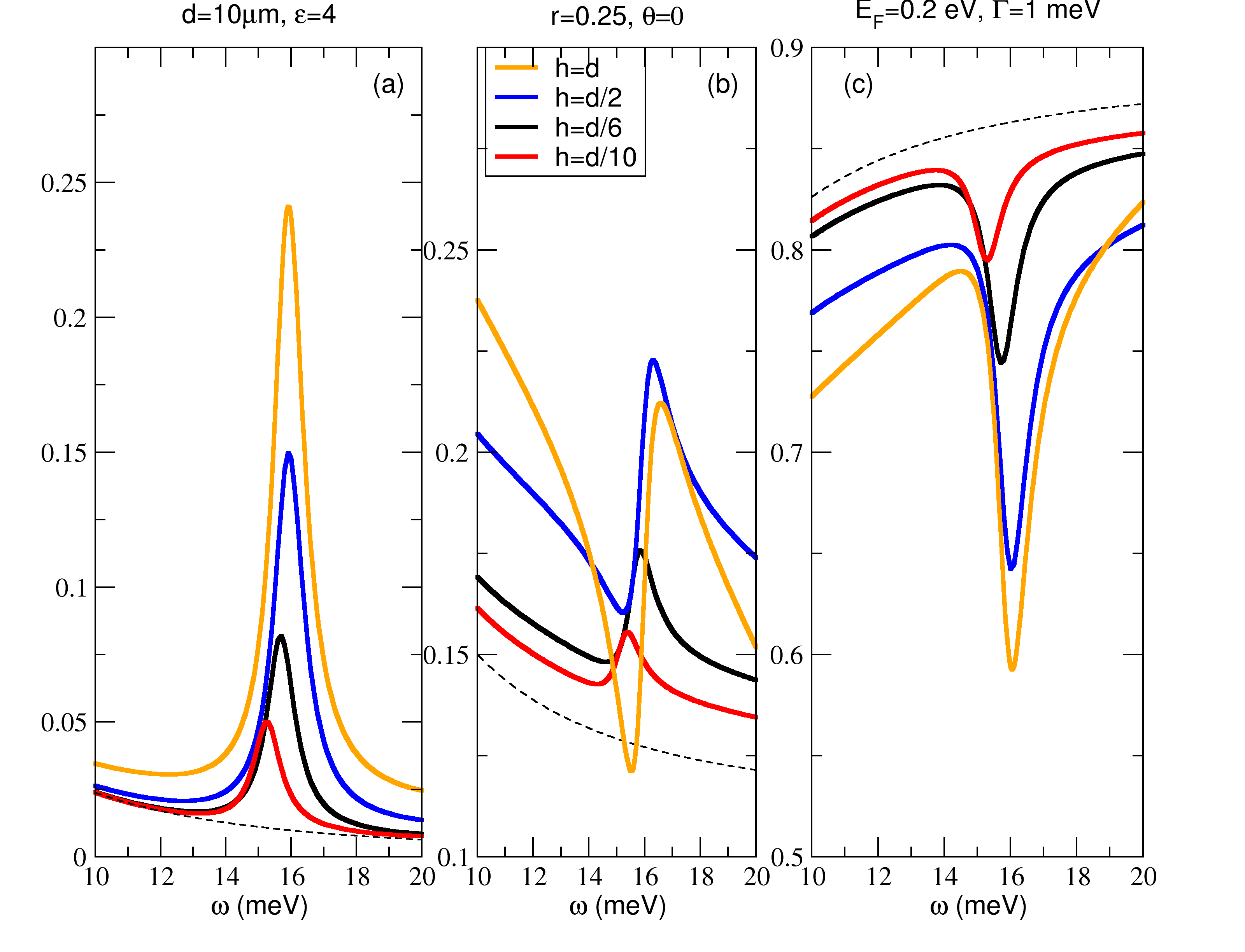
The effect of increasing the depth of the grooves, from up to is to produce an enhancement of the absorption, which for is almost of (in this case we are considering ).
The dispersion of a surface plasmon-polaritons in graphene, when the sheet is sandwiched between two semi-infinite dielectrics, is, in the electrostatic limit, given by[38]
| (66) |
where
| (67) |
and . Taking , the smallest lattice wavevector, Eq. (66) predicts, for the parameters used in our calculation, a plasmon-polariton energy of
| (68) |
which is in the ballpark of the numeric result. We should however note that the position of the resonance depends also on the parameter , which is not captured by the above formula for the dispersion. We can include the effect of the parameter using an interpolative formula. We define a new as
| (69) |
Using this formula we obtain
| (70) |
a much better approximation to the numerical value (15.9 meV). To obtain the exact frequency of the resonance we have to compute the plasmonic band structure due to the periodic dielectric, that is, the band structure of a polaritonic crystal.[39] In the Appendix B we give the polaritonic band structure of graphene on a square-wave grating.
In Fig. 4 we depict the absorbance (a), reflectance (b), and transmittance (c), as function of frequency, for different values of , from up to , and keeping , that is the limit of deep grooves. As increases the position of the resonance shifts to the left. This happens because the width of the dielectric underneath graphene is increasing with . Then, according to Eq. (67), the effective dielectric constant of the system increases, following from Eq. (66) that the resonance shifts toward lower energies.

In the case of two resonances are seen in the frequency window considered. They correspond to the excitation of surface plasmon-polaritons of wave numbers and . Then, according to Eq. (66), the position of the second resonance should be times the first resonance frequency. From the figure, the energy of the first resonance is meV, while that of the second one is meV; now we note that meV, in agreement with the numerical result. We also note that the absorption of graphene is largest when , the symmetric case (), reaching a value higher than . Although we do not show it here, we have found that the absorption grows monotonically with increasing and attains a maximum at a value larger than 45% for .
Finally, we note that the reflectance curves have Fano-type shape.[39] This is due to the coupling of the external radiation field with the excitation of Bragg modes of surface plasmon-polaritons in periodically modulated structures.
An important quantity when dealing with plasmonic effects is the enhancement of the electromagnetic field close to the interface of the metal (in this case graphene) and the dielectric (the square-wave grating). The spatial intensity of the diffracted electromagnetic field from graphene is depicted in Fig.5. For the case off-resonance [Fig.5(a)] the magnetic field has a relatively small amplitude and is almost homogeneous along -axis, while along -axis exhibits a discontinuity at the plane occupied by the graphene layer, in accordance with the boundary conditions.
The situation changes dramatically when the incident wave frequency coincides with that of a surface plasmon-polariton resonance [Figs.5(b–d)]. In this case the amplitude of the electromagnetic field in the vicinity of the graphene layer drastically increases. The electromagnetic field amplitude is maximal when the surface plasmon-polariton resonance occurs for the first harmonic [Fig.5(b)], that is for , while it gradually decreases as the harmonic’s order increases (compare with Fig.5(c) for second and Fig.5(d) for third harmonics, respectively). It is this enhancement of the electromagnetic field due to the excitation of surface plamons-polaritons in the vicinity of a metallic interface that is at the heart of sensing devices.

VI Modulated doping: a simple model
As discussed in the Introduction, doping graphene using a bottom gate when the material lies on a grating leads to a position dependent conductivity, which is periodic along the direction. In this section we consider a simple model where, in addition to the grating itself, the conductivity is position dependent and periodic. In our model the conductivity is given by[38]
| (71) |
where is a parameter controlling the degree of inhomogeneity. We also take in our figures. This particular choice of and makes the latter commensurate with the profile of the grating. From the point of view of the calculation we have to replace by in the formulas given above. The conductivity is then expanded in Fourier series as
| (72) |
where
| (73) |
For the case of the profile defined in Eq. (71) the Fourier series reduces to three terms only, those referring to . A non-sinusoidal profile for will have more harmonics than just these three. Therefore, our model can also be considered the first term in the Fourier expansion of a more complex profile for .
Relatively to the previous case of homogeneous conductivity, what changes in the equations is the form of the function , which now reads
| (74) |
where
| (75) |

The results for the absorbance, reflectance, and transmittance are given in Fig. 6, considering the case where , a fairly large value, corresponding to deep groves. The dashed line is the case where graphene has an inhomogeneous conductivity on top of a homogeneous dielectric (i.e., no grating). (This situation is artificial and is only included for the sake of comparison.) Two resonant peaks can be seen, with the second peak being much smaller than the one at lower energies. The dashed-dotted line is the case where we have homogeneous graphene on the grating, and the solid line corresponds to the case where we have graphene with an inhomogeneous conductivity on the grating. The main effect is a shift of the position of the resonant peaks toward lower energies and an enhancement of the absorption, which bears its origin on the combined effect of the grating and of the periodic modulation of the conductivity. In the absorbance panel the energy of the resonance labelled (2) is larger than that of the resonance (1). Thus, the first resonance corresponds to an excitation of a surface plasmon-polariton of wave number whereas the second peak corresponds to the excitation of surface plasmon-polariton of wave number . When we compare the dashed curve to the solid one we also note the prominence of the second plasmonic peak in the latter case, which is almost as intense as the low energy one. This is a consequence of the square profile and the dielectric nature of the grating. In metallic gratings the permittivity has a strong frequency dependence favouring the the occurence of the most intense plasmonic resonances at lower energies.[40]
VII Conclusions and future work
We have shown that a flat sheet of graphene on top of a square-wave grating exhibits strong plasmonic behavior. With the help of the grating one can create a surface plasmon-polariton resonance. The effect is more pronounced in the case of deep grooves, where absorbances higher than are attainable. We note that the parameter is easy to control experimentally, providing a convenient way of tuning the position of the plasmonic resonance. The reflectance curves show a Fano-type line shape, which is manifest of the coupling of the external electromagnetic field (with a continuum of modes) to the surface plasmons in graphene (occupying a relatively narrow spectral band). The calculations we have performed assume that graphene is homogeneously doped (excluding Sec. VI), which is a crude approximation for the case of a bottom gate configuration of graphene doping. Therefore, our results are only directly applicable to the cases of either chemical doping or doping by a top gate. This type of gating is within the state-of-the-art.[64] In the particular case of bottom gate, we have to consider both the effect of inhomogeneous doping and the effect of strain (if the grooves are not filled with another dielectric). Both effects result in a position dependent conductivity. Then, the calculation of the properties of surface plasmon-polaritons requires the evaluation of the doping profile and the strain field. Once these are determined, one can use a Fourier expansion of the graphene conductivity as we have considered in our phenomenological model. As these preliminary results show, the coupling of the external wave to the surface plasmon-polaritons can be significantly enhanced in the presence of both the dielectric grating and periodic modulation of the conductivity. Detailed calculations for realistic graphene conductivity profiles are the goal of a future work.
Acknowledgements
NMRP acknowledges Bao Qiaoliang, José Viana-Gomes, and João Pedro Alpuim for fruitful discussions. A. F. was supported by the National Research Foundation–Competitive Research Programme award “Novel 2D materials with tailored properties: beyond graphene” (Grant No. R-144-000-295-281). This work was partially supported by the Portuguese Foundation for Science and Technology (FCT) through Projects PEst-C/FIS/UI0607/2011 and PTDC-FIS-113199-2009.
Appendix A Explicit form of
The calculation of the integral in Eq. (61) has to be divided into two pieces. The function can be written as
| (76) |
where
| (77) | |||||
and
| (78) | |||||
Since the square profile has a piecewise structure, the function is obtained directly from the function as
| (79) |
Appendix B Polaritonic spectrum
The polaritonic spectrum, , of the surface plasmons-polaritons (SPP) in graphene on a square-wave grating is represented in Fig.7, where is the Bloch wavenumber. Here, and in order to avoid the appearance of an imaginary part of the eigenvalues, corresponding to surface plasmon-polariton damping, we considered graphene without disorder (). As expected, the periodicity of the grating induces a band structure in the SPP spectrum of graphene, showing energy gaps. At the same time, for normal incidence () the frequency of the second band (meV) almost coincides with the numerically obtained resonant frequency meV. A similar good agreement happens for the frequency of fifth band and that of second resonance (meV and meV, respectively), as well as for frequency of sixth band and that of third resonance (meV and meV, respectively).

References
- [1] A. H. Castro Neto, F. Guinea, N. M. R. Peres, K. S. Novoselov, and A. K. Geim, Rev. Mod. Phys. 81, 109 (2009).
- [2] N. M. R. Peres, Rev. Mod. Phys. 82, 2673 (2010).
- [3] S. D. Sarma, S. Adam, E. H. Hwang, and E. Rossi, Rev. Mod. Phys. 83, 407 (2011).
- [4] N. M. R. Peres, F. Guinea, and A. H. Castro Neto, Phys. Rev. B 73, 125411 (2006).
- [5] L. A. Falkovsky and S. S. Pershoguba, Phys. Rev. B 76, 153410 (2007).
- [6] T. Stauber, N. M. R. Peres, and F. Guinea, Phys. Rev. B 76, 205423 (2007).
- [7] T. Stauber, N. M. R. Peres, and A. H. Castro Neto, Phys. Rev. B 78, 085418 (2008a).
- [8] T. Stauber, N. M. R. Peres, and A. K. Geim, Phys. Rev. B 78, 085432 (2008b).
- [9] V. P. Gusynin, S. G. Sharapov, and J. P. Carbotte, New J. Phys. 11, 095013 (2009).
- [10] A. G. Grushin, B. Valenzuela, and M. A. H. Vozmediano, Phys. Rev. B 80, 155417 (2009).
- [11] E. G. Mishchenko, Phys. Rev. Lett. 103, 246802 (2009).
- [12] L. Yang, J. Deslippe, C.-H. Park, M. L. Cohen, and S. G. Louie, Phys. Rev. Lett. 103, 186802 (2009).
- [13] N. M. R. Peres, R. M. Ribeiro, and A. H. Castro Neto, Phys. Rev. Lett. 105, 055501 (2010).
- [14] A. Ferreira, J. Viana-Gomes, Y. V. Bludov, V. M. Pereira, N. M. R. Peres, and A. H. Castro Neto, Phys. Rev. B 84, 235410 (2011).
- [15] J.-T. Liu, N.-H. Liu, J. Li, X. J. Li, and J.-H. Huang, Appl. Phys. Lett. 101, 052104 (2012).
- [16] M. Busl, G. Platero, and A.-P. Jauho, Phys. Rev. B 85, 155449 (2012).
- [17] R. R. Nair, P. Blake, A. N. Grigorenko, K. S. Novoselov, T. J. Booth, T. Stauber, N. M. R. Peres, and A. Geim, Science 320, 1308 (2008).
- [18] A. B. Kuzmenko, E. van Heumen, F. Carbone, and D. van der Marel, Phys. Rev. Lett. 100, 117401 (2008).
- [19] K. F. Mak, M. Y. Sfeir, Y. Wu, C. H. Lui, J. A. Misewich, and T. F. Heinz, Phys. Rev. Lett. 101, 196405 (2008).
- [20] Z. Q. Li, E. Henriksen, Z. Jiang, Z. Hao, M. C. Martin, P. Kim, H. Stormer, and D. Basov, Nature Phys. 4, 532 (2008).
- [21] F. Wang, Y. Zhang, C. Tian, C. Girit, A. Zettl, M. Crommie, and Y. R. Shen, Science 320, 206 (2008).
- [22] A. B. Kuzmenko, I. Crassee, D. van der Marel, P. Blake, and K. S. Novoselov, Phys. Rev. B 80, 165406 (2009).
- [23] I. Crassee, J. Levallois, A. L. Walter, M. Ostler, A. Bostwick, E. Rotenberg, T. Seyller, D. van der Marel, and A. B. Kuzmenko, Nat. Phys. 7, 48 (2011).
- [24] Q. Bao, H. Zhang, B. Wang, Z. Ni, C. H. Y. X. Lim, Y. Wang, D. Y. Tang, and K. P. Loh, Nature Photonics 5, 411 (2011).
- [25] J. M. Dawlaty, S. Shivaraman, J. Strait1, P. George, M. Chandrashekhar, F. Rana, M. G. Spencer, D. Veksler, and Y. Chen, Appl. Phys. Lett. 93, 131905 (2008).
- [26] H. Yan, F. Xia, W. Zhu, M. Freitag, C. Dimitrakopoulos, A. A. Bol, G. Tulevski, and P. Avouris, ACS Nano 5, 9854 (2011).
- [27] L. Ren, Q. Zhang, S. Nanot, I. Kawayama, M. Tonouchi, and J. Kono, Journal of Infrared, Millimeter, and Terahertz Waves 33, 846 (2012a).
- [28] L. Ren, Q. Zhang, J. Yao, Z. Sun, R. Kaneko, Z. Yan, S. L. Nanot, Z. Jin, I. Kawayama, M. Tonouchi, et al., Nano Lett. 12, 3711 (2012b).
- [29] M. Tonouchi, Nature Photonics 1, 97 (2007).
- [30] H. Yan, X. Li, B. Chandra, G. Tulevski, Y. Wu, M. Freitag, W. Zhu, P. Avouris, and F. Xia, Nature Nano. 7, 330 (2012).
- [31] J. Chen, M. Badioli, P. Alonso-Gonzalez, S. Thongrattanasiri, F. Huth, J. Osmond, M. Spasenovic, A. Centeno, A. Pesquera, P. Godignon, et al., Nature 487, 77 (2012).
- [32] G. Konstantatos, M. Badioli, L. Gaudreau, J. Osmond, M. Bernechea, P. G. de Arquer, F. Gatti, and F. H. L. Koppens, Nature Nanotechnology 7, 363 (2012).
- [33] Z. Fei, G. O. Andreev, W. Bao, L. M. Zhang, A. S. McLeod, C. Wang, M. K. Stewart, Z. Zhao, G. Dominguez, M. Thiemens, et al., Nano Lett. 11, 4701 (2011).
- [34] Z. Fei, A. S. Rodin, G. O. Andreev, W. Bao, A. S. McLeod, M. Wagner, L. M. Zhang, Z. Zhao, G. Dominguez, M. Thiemens, et al., Nature 487, 82 (2012).
- [35] L. Vicarelli, M. S. Vitiello, D. Coquillat, A. Lombardo, A. C. Ferrari, W. Knap, M. Polini, V. Pellegrini, and A. Tredicucci, Nature Materials 11, 865 (2012).
- [36] I. Crassee, M. Orlita, M. Potemski, A. L. Walter, M. Ostler, T. Seyller, I. Gaponenko, J. Chen, and A. B. Kuzmenko, Nano Lett. 12, 2470 (2012).
- [37] T. J. Echtermeyer, L. Britnell, P. K. Jasnos, A. Lombardo, R. V. Gorbachev, A. N. Grigorenko, A. K. Geim, A. C. Ferrari, and K. S. Novoselov, Nature Communications 2, 458 (2011).
- [38] N. M. R. Peres, A. Ferreira, Y. V. Bludov, and M. I. Vasilevskiy, J. Phys.: Condens. Matter 24, 245303 (2012).
- [39] Y. V. Bludov, N. M. R. Peres, and M. I. Vasilevskiy, Phys. Rev. B 85, 245409 (2012a).
- [40] A. Ferreira and N. M. R. Peres, Phys. Rev. B 86, 205401 (2012).
- [41] W. Gao, J. Shu, C. Qiu, and Q. Xu, ACS Nano 6, 7806 (2012).
- [42] A. Ferreira, N. M. R. Peres, R. M. Ribeiro, and T. Stauber, Phys. Rev. B 85, 115438 (2012).
- [43] M. Furchi, A. Urich, A. Pospischil, G. Lilley, K. Unterrainer, H. Detz, P. Klang, A. M. Andrews, W. Schrenk, G. Strasser, et al., Nano Letters 12, 2773 (2012).
- [44] A. A. Dubinov, V. Y. Aleshkin, V. Mitin, T. Otsuji, and V. Ryzhii, J. Phys.: Condens. Matter 23, 145302 (2011).
- [45] J. Zhang, L. Zhang, and W. Xu, J. Phys. D: Appl. Phys. 45, 113001 (2012).
- [46] A. N. Grigorenko, M. Polini, and K. S. Novoselov, Nature Photonics 6, 749 (2012).
- [47] P. Tassin, T. Koschny, M. Kafesaki, and C. M. Soukoulis, Nature Photonics 6, 259 (2012).
- [48] F. Bonaccorso, Z. Sun, T. Hasan, and A. C. Ferrari, Nature Photonics 4, 611 (2010).
- [49] Q. Bao and K. P. Loh, ACS Nano 6, 3677 (2012).
- [50] B. Sensale-Rodriguez, R. Yan, S. Rafique, M. Zhu, W. Li, X. Liang, D. Gundlach, V. Protasenko, M. M. Kelly, D. Jena, et al., Nano Lett. 12, 4518 (2012).
- [51] Y. V. Bludov, M. I. Vasilevskiy, and N. M. R. Peres, EuroPhys. Lett. 92, 68001 (2010).
- [52] Y. V. Bludov, M. I. Vasilevskiy, and N. M. R. Peres, J. Appl. Phys. 112, 084320 (2012b).
- [53] Y. Zhou and M. W. Wu, Phys. Rev. B 83, 245436 (2011).
- [54] S. A. Mikhailov, Europhys. Lett. 79, 27002 (2007).
- [55] S. A. Mikhailov and K. Ziegler, J. Phys.: Condens. Matter 20, 384204 (2008).
- [56] S. A. Mikhailov, Microelectronics Journal 40, 712 (2009).
- [57] L. A. Falkovsky, J. Phys.: Conf. Ser. 129, 012004 (2008).
- [58] J. Horng, C.-F. Chen, B. Geng, C. Girit, Y. Zhang, Z. Hao, H. A. Bechtel, M. Martin, A. Zettl, M. F. Crommie, et al., Phys. Rev. B 83, 165113 (2011).
- [59] J. Chandezon, D. Maystre, and G. Raoult, J. Optics 11, 235 (1980).
- [60] L. Li, J. Chandezon, G. Granet, and J.-P. Plumey, Applied Optics 38, 304 (1999).
- [61] P. Sheng, R. S. Stepleman, and P. N. Sanda, Phys. Rev. B 26, 2907 (1982).
- [62] S. Tongay, K. Berke, M. Lemaitre, Z. Nasrollahi, D. B. Tanner, A. F. Hebard1, and B. R. Appleton, Nanotechnology 22, 425701 (2011).
- [63] H. Liu, Y. Liu, and D. Zhu, J. Mater. Chem. 21, 3335 (2011).
- [64] L. Ju, B. Geng, J. Horng, C. Girit, M. C. Martin, Z. Hao, H. A. Bechtel, X. Liang, A. Zettl, Y. R. Shen, et al., Nature Nanotechnology 6, 630 (2011).