Quantum Hall effect in graphene with twisted bilayer stripe defects
Abstract
We analyze the quantum Hall effect in single layer graphene with bilayer stripe defects. Such defects are often encountered at steps in the substrate of graphene grown on silicon carbide. We show that AB or AA stacked bilayer stripes result in large Hall conductivity fluctuations that destroy the quantum Hall plateaux. The fluctuations are a result of the coupling of edge states at opposite edges through currents traversing the stripe. Upon rotation of the second layer with respect to the continuous monolayer (a twisted-bilayer stripe defect), such currents decouple from the extended edge states and develop into long-lived discrete quasi bound states circulating around the perimeter of the stripe. Backscattering of edge modes then occurs only at precise resonant energies, and hence the quantum Hall plateaux are recovered as twist angle grows.
pacs
73.50.Jt 72.80.Vp 85.75.NnI Introduction
The unique half-integer quantum Hall effect (QHE) in monolayer graphene serves as a fingerprint of massless Dirac electrons. [1, 2] It is therefore used in the laboratory to distinguish monolayers from multilayers. [3] The electrons in graphene under applied perpendicular magnetic field have an unconventional Landau level spectrum, leading to a sequence of Hall conductivity plateaux , where is the conductance quantum, (h is Planck’s constant and e is the electron charge), and is an integer including zero. [4] The large energy level separation between the and Landau levels adds robustness to the plateau, which has been observed also at room temperature. [5] More importantly, measurements [6, 7, 8] of the von Klitzing constant have been performed to metrological accuracy on epitaxial graphene on silicon-carbide (SiC). Large break-down currents have been observed for this material, and epitaxial graphene at present outperforms conventional two-dimensional electron gases in semiconducting heterostructures in this respect, and may very well be the material of choice for metrology in the future. Transistors with promising high cut-off frequencies have also been fabricated from epitaxial graphene. [9, 10] It is therefore of high current interest to establish the electron transport properties of graphene on SiC. [11]
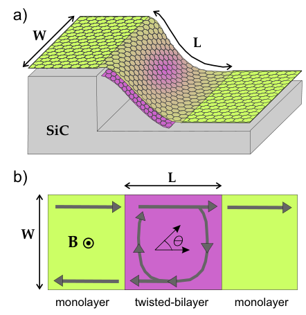
Inhomogeneities in the two-dimensional material are often detrimental to its transport properties. [12, 13, 14, 15, 16] Epitaxial graphene on SiC may continuously cover the whole SiC substrate, [17, 18, 19] but steps on the substrate influence the graphene layer along lines running across the wafer. [20, 21] At a step, the graphene sheet may be more decoupled from the underlaying substrate than on the wide terraces between steps, which may change the doping level locally. [20, 22] Graphene may also suffer strain [23] since the SiC step is atomically sharp, while the graphene sheet forms a continuous cover. In addition, since the steps serve as seeds in the growth process of epitaxial graphene, bilayers or multilayers are often observed, [24, 25, 19] see Fig. 1 (a). Depending on the growth process, several islands may form near the steps or continuous stripes may be formed along a large part of the step. After fabrication of the Hall bar, the bilayer stripe defects can reach from one side to the other of the Hall bar, resulting in a geometry similar to the one shown in Fig. 1 (b). Experimentally, it was recently observed [26] that narrow Hall bars intentionally fabricated perpendicular or parallel to steps display markedly different properties. When the current path crosses many steps, a positive magnetoresistance arises, that can be explained, according to Schumann et al., [26] as the result of Hall edge channel backscattering caused by new edge channels developing along the substrate steps, although the specific mechanism remains an open question. In contrast, other experiments [19, 27, 28] show that the magnetotransport in epitaxial graphene appears basically insensitive to surface steps. Thus, a theory that embraces both scenarios is still missing.
Here, we numerically investigate a scenario that reconciles both observations, wherein a bilayer patch interferes with the currents flowing in the underlaying monolayer, as sketched in Fig. 1 (b). We show that the QHE plateau quantization is strongly suppressed by the presence of a single AA- or AB-stacked bilayer stripe crossing the Hall bar, which opens up the possibility of edge state backscattering by connecting opposite edges. This effect, however, becomes much weaker as the two layers are rotated by a finite relative angle, breaking the perfect AA or AB stacking. We find that the QHE is least distorted as the twist angle approaches (midway between AA and AB stacking). Although inter-edge backscattering remains possible in this case, it becomes confined to narrow resonances, apparent as narrow dips in the Hall plateaux, and caused by quasi-bound states circulating around the patch that are weakly coupled to the extended edge states. The backscattering resonances are furthermore smeared out by finite temperature effects. Hence, a significant suppression of Hall plateaux in SiC-grown epitaxial graphene typically requires the Hall bar to lie across substrate steps, as found in Ref. 26, but also good crystallographic alignment of the multilayer patches seeded by the steps.
II Hall effect across a twisted bilayer
The properties of bilayer graphene, particularly of twisted bilayers, have been the focus of considerable interest recently. [29, 30, 31, 32] For AB-stacked bilayer graphene, the two Dirac cones of a decoupled double monolayer system are strongly modified by the interlayer hopping, resulting in parabolic bands and possibly trigonal warping. [33] In twisted graphene, on the other hand, the two cones within each valley are separated in reciprocal space and interlayer coupling leads to a finite energy saddle point in the band structure at the intersection of the two surviving Dirac cones. The corresponding van Hove singularity has been observed experimentally. [34] The question arises as to what the QHE looks like across a monolayer-bilayer graphene junction, including the effect of interlayer twist in the bilayer part.
It should be recognized that a heterostructure[35] consisting of monolayer graphene occupying the half space and bilayer graphene occupying the other half space is rather different from the geometry considered in this paper, where the bilayer exists between , see Fig. 1, and plays the role of a complicated barrier for electron flow in the lower extended monolayer. The finite length of the bilayer patch leads to the formation of a spectrum with quasi-bound state resonances. Such states are chiral and circulate around the perimeter of the patch, but may escape into the two extended states at opposite edges of the monolayer (and eventually to reservoirs) through two opposite corners of the patch [see Fig. 1 (b)]. When the Fermi energy equals a resonance energy, a vertically propagating channel is opened that connects an incoming edge state into an outgoing state at the opposite edge, allowing for backscattering in the QHE regime. This appears as a dip of depth in the quantized value of the Hall conductivity across the resonance. If the width of the resonance levels exceeds the corresponding level separation, the Hall conductivity plateaux are completely destroyed. Ultimately, the existence of such transverse backscattering channels has a topological origin, since the different Chern-numbers of the monolayer and bilayer bands dictates that the number of edge channels along a monolayer-bilayer interface is odd, as a consequence of the bulk-surface correspondence. [36, 37]

II.1 Model
To illustrate the resonant backscattering effect, we have performed quantum transport calculations for two-terminal and six-terminal nano-ribbon devices in a magnetic field. We ignore the effects of inhomogenous doping and strain, which may also modify magnetotransport as studied elsewhere, [23] and concentrate on the effect of a bilayer patch. The starting point is the tight-binding Hamiltonian for graphene
| (1) |
where the hopping elements include hopping beyond nearest neighbors, and are modeled by the -orbital overlap at different carbon sites and separated by ,
| (2) |
Here, and are the nearest neighbor and interlayer hopping parameters of graphite, is the carbon-carbon distance in-plane and is the interlayer distance. The exponent is . The formula in Eq. (2) is applied for atomic distances reaching a cut-off , beyond which . This generalization beyond simple nearest-neighbor models is crucial to properly recover the low energy electronic structure of twisted bilayers, in particular its gapless and valley-decoupled double-cone spectrum, as described by the continuum theory of Ref. 29. In practice, a rather precise description at relevant energy scales is obtained for .
II.2 Bandstructure of the leads
The band structure of the monolayer graphene nanoribbon leads converges rapidly with increasing hopping cut-off , and is shown for a 10 nm wide zigzag nanoribbon with in Fig. 2 for varying magnetic fields. The magnetic field is included in the model through a standard Peierl’s substitution. We note that for large , a large unit cell of length is needed for which the first Brillouin zone in reciprocal space is small. This correlates with the folding of the bands of a nearest neighbor tight-binding model but leads to slightly more complicated bands due to the long range hoppings, see Fig. 2. For instance, for small magnetic fields, Fig. 2(a), we see a positive energy shift of the cones of about and the zero-energy edge modes of the zigzag ribbon display substantial dispersion.[38] For small magnetic fields the magnetic length is larger or comparable to the ribbon width and the spectrum is dominated by size quantization. This is the case in Fig. 2(a) where the energy split of the zero-mode is due to the small magnetic field corresponding to a flux per hexagon, where is the magnetic flux quantum. For larger fields, the Landau levels ( is the Dirac electron velocity in the absence of magnetic field) become visible as flat regions in the dispersion. The dispersive parts of the bands correspond to edge modes, carrying the current in the quantum Hall regime.


III Magnetotransport simulation
To evaluate the effect of the bilayer patch, we compute magnetotransport properties using recursive Green’s function (RGF) techniques, [39, 40] where the coupling to reservoirs are included through self-energies derived from the surface Green’s functions of semi-infinite leads. The leads and the system are modeled on equal footing through the Hamiltonian in Eq. (1). The RGF algorithm gives the retarded Green’s function of the system. Such Green’s function is obtained, between certain pairs of points, by iterative application of the Dyson equation, and may be then used to compute the Hall conductivity, the current densities or the scattering matrix of the system. The recursive iteration is performed on slices of the lattice that are connected only to neighboring slices, and which hence increase in size as the hopping cut-off increases. This has a rather steep computational cost, but has the advantage that it cleanly avoids fermion doubling problems that plague strategies based on the discretization of low energy effective theories in graphene, and can moreover quantitatively incorporate the precise edge termination of each of the Hall bar regions.
III.1 Multiterminal Hall conductivity
In Fig. 3 we display a 6-terminal monolayer graphene Hall bar device with six contacts (leads) enumerated by L1-L6. In a typical experiment, a current is sent from L1 to L2, and the voltage between L3 and L5 gives the longitudinal resistance, while the Hall resistance is obtained by measuring the transverse voltage between for instance L5 and L6. Since this Hall bar is of monolayer graphene only, it is sufficient to use a nearest neighbor model. After computation of the full scattering matrix connecting the six leads, we compute the longitudinal resistance and the transverse conductance in the linear response regime. We display both in (c) as function of Fermi energy of the system (related to the electron density). The transverse conductance display quantized values , where and This sequence is characteristic for the monolayer quantum Hall effect. The longitudinal resistance is zero except at the steps between plateaux. The random fluctuations at the steps are due to the added randomness of 10% of the nearest neighbor hopping integral around in this simulation.
The current flows along edge states, as is clearly seen in Fig. 3(a), which shows the local current flow patterns throughout the device when currents are injected at L6 and L1 and subsequently collected at L4 and L3. In Fig. 3(b) we show the current redistribution throughout the entire device that appears at each step between plateaux (in this case the and plateaux at ).
In Fig. 4 we show the influence of an AB-stacked bilayer stripe defect placed in the middle and connecting the two edges of the Hall bar. The current can now enter into a circular path around the bilayer patch and eventually go out into both leads L5 and L4, see Fig. 4(a). This leads to large fluctuations of the longitudinal resistance , as shown in Fig. 4(a), red circles. At the same time, the transverse conductance is affected. If the voltage probes are set between L5 and L6, the influence of the patch is minimal. On the other hand, when the voltage probes span the patch, for instance when they are placed between L3 and L6, the fluctuations are added into as well, and the plateaux are destroyed.

III.2 Two-terminal conductance and twist angle
Next we study the influence of a finite twist angle on the fluctuations of the Hall conductance. In contrast to the AB-stacked bilayer patch explored above, this requires that we include long-range hopping with a cut-off . For this study it is convenient to limit the calculations to a two-terminal set-up, as in Fig. 1(b). In the absence of contact resistances, like in the present case, the two-terminal conductance equals the Hall conductivity . In Fig. 5 we show the conductance for a nm wide ribbon in a quantizing magnetic field as function of Fermi energy (i.e. doping). The bandstructure of the underlaying monolayer is shown in Fig. 2(d). The bilayer patch length is nm. The twist angle corresponds to a bilayer patch with AB stacking, while would correspond to AA stacking. For small twist angles, all plateaux are destroyed by backscattering caused by a number of resonance states in the patch, which are rather broad and tend to overlap. For increasing twist angle, these resonances become sharper, signaling a decoupling of the quasibound states from the edge modes in the underlying monolayer that is connected to source and drain reservoirs. The plateaux become better defined, starting with the plateau at small twist angle and continuing with the higher Landau level index plateaux at higher twist angles (higher index require larger twist angle to recover). 11 1 Note that the peak in Fig. 5 around (in the zeroth plateau), is related to the dispersive zero mode characteristic of the zig-zag nanoribbon of Fig. 2(d).
The dependence with twist angle of the width of the backscattering resonances, or in other words, of the coupling between the corresponding quasibound state and the monolayer edge states, can be traced to the band structure of the twisted bilayer. In the limit of a vanishing interlayer coupling , the states become perfectly bound and lie fully on the decoupled layer. Their momentum components are concentrated around the Dirac point of said layer. In contrast, the delocalized edge states in the extended monolayer are spectrally concentrated around the monolayer Dirac point, which has a shift [for ] with respect to the former. The momentum spread grows linearly with energy. Therefore, for a given energy, the larger the momentum mismatch of the two Dirac points, the smaller the overlap between delocalized edge states and localized patch states will be. Since this overlap is a measure of the inverse lifetime of the quasibound state in the limit of small , we see that twist angles around (half-way between AB and AA stacking, maximum ) will correspond to least coupling, narrower resonances, and cleaner Hall plateaux, as seen in Fig. 5.
A second consequence of this analysis is that, as soon as the Fermi energy approaches the van Hove singularity where the two Dirac cones intersect (at energy ), the spectral spread becomes comparable to , so the overlap will increase greatly, and the backscattering will be enhanced. Hence, higher Hall plateaux will be eventually destroyed for any value of the twist angle as the filling factor grows. This is also apparent in Fig. 5(a). For instance, for (blue curve), it is clear that the and plateaux have sharp resonances, while plateau and especially plateaux at higher doping (i.e. higher ) are destroyed.
III.3 Circulating quasi-bound states
To demonstrate the connection between resonant backscattering and quasibound states of circulating currents around the patch, we present in Fig. 6 the local current flow pattern throughout the system for filling factors near and at the resonance dip indicated by the blue arrow in Fig. 5(b). In the first panel the edge current flows from left to right, from source to drain, along the upper edge in the Landau level of the monolayer undisturbed by the patch. On resonance (fourth panel) the current circulates in the patch and suffers perfect back reflection at the lower edge (blue back-flowing current), and the conductance from such edge state is zero on resonance. Similar resonances occur at higher plateaux, where resonant backscattering from each patch state always removes at most one conductance quantum from the Hall conductivity (assuming unbroken spin symmetry).

III.4 Effects of Disorder
In the above two-termainal simulations of the bilayer stripe defect we have neglected disorder. A simple model of disorder was included in the 6-terminal simulations in Section III.1 through a randomization of the nearest neighbor hopping integrals around in that case. To simulate the influence of disorder on the conductance fluctuations induced by the bilayer patch, we do the same for the in Eq. (2). In practice, we make the substitution , where the level of disorder is and is a random number between and . In Fig. 7 we show results of this type of disorder for a bilayer patch with twist angle for energies , which is on the plateau in Fig. 5. We vary the disorder strength from to , with the same random number sequence . For small disorder strength, the resonances are shifted in energy. For increasing disorder strength (bigger ), resonances get broadened. Eventually, resonances overlap and the plateau is completely destroyed again, despite its twist angle. This destruction can be understood as due to enhanced momentum relaxation that reduces the effect of the momentum mismatch between the Dirac cones of the two layers that in the first place (without disorder) decoupled the layers and lead to sharp resonances. We find, thus, that a sizeable amount of disorder is necessary to cause an appreciable correction to the general results found in the clean case.
IV Conclusions and Outlook
We have analyzed the effect of bilayer stripes transverse to graphene Hall bars on the Hall conductivity. Such stripes are observed to naturally arise at substrate steps in epitaxially grown graphene. We have found that, in agreement with Ref. 26, the Hall plateaux are destroyed by the coupling between opposite edge states via transverse transport channels circulating around the bilayer perimeter. Such channels arise as a result of the jump in Chern number between the band structures of bilayer and monolayer graphene, and give rise to the formation of circulating quasibound states in finite length bilayer patches. Hall plateaux develop backscattering resonances, visible as dips of depth one conductance quantum, whenever the Fermi energy crosses a quasi bound level in the patch. The width of the backscattering resonances diminishes as the bilayer twist angle approaches , which leads to well defined low energy plateaux despite the patch. However, resonance width grows with Fermi energy, completely spoiling Hall plateaux above the van Hove singularity of the twisted bilayer patch. Both features are explained in terms of the momentum mismatch between the Dirac cones in the two layers. We propose that this scattering mechanism should be relevant in understanding deviations of the QHE in epitaxial graphene Hall bars etched across SiC steps, like the anomalous positive magnetoresistance and non-quantized Hall plateaux in Ref. 26.
In this first study of such Hall bars, sketched in Fig. 1(a), we have neglected effects of strain, inhomogeneous doping, and the possibility of a Zeeman term due to an in-plane component of the magnetic field. In addition, we have neglected electron-electron interactions that may lead to wider wavefunctions of the edge states [the current paths in for instance Fig. 3(a)]. The relavance of these effects, which should be present at least to some extent in real experiments, are left as future work. However, our expectation is that, since the essential mechanism for the low energy protection of Hall plateux found in our work stems from the momentum mismatch between layers, the destructive effect of inhomogeneities, including those arising from strain and screening, will be small, as long as their characteristic lengthscales are greater than the Moiré period of the twisted bilayer patch .
Acknowledgements.
We acknowledge financial support from the EU through FP7 STREP ConceptGraphene (T.L.), the Swedish Foundation for Strategic Research (T.L.), the CSIC JAE-Doc program and the Spanish Ministry of Science and Innovation through Grant No. FIS2011-23713 (P.S.-J) and FIS2009-08744 (E.P.), and the European Research Council Advanced Grant, contract 290846 (P. S-J.). This research was supported in part by the National Science Foundation under Grant No. NSF PHY05-51164.References
- [1] K. S. Novoselov, A. K. Geim, S. V. Morozov, D. Jiang, M. I. Katsnelson, I. V. Grigorieva, S. V. Dubonos, and A. A. Firsov, Nature 438, 197 (11 2005)
- [2] Y. Zhang, Y.-W. Tan, H. L. Stormer, and P. Kim, Nature 438, 201 (11 2005)
- [3] K. S. Novoselov, E. McCann, S. V. Morozov, V. I. Fal’ko, M. I. Katsnelson, U. Zeitler, D. Jiang, F. Schedin, and A. K. Geim, Nat. Phys. 2, 177 (03 2006)
- [4] V. P. Gusynin and S. G. Sharapov, Phys. Rev. Lett. 95, 146801 (Sep 2005)
- [5] K. S. Novoselov, Z. Jiang, Y. Zhang, S. V. Morozov, H. L. Stormer, U. Zeitler, J. C. Maan, G. S. Boebinger, P. Kim, and A. K. Geim, Science 315, 1379 (2007)
- [6] A. Tzalenchuk, S. Lara-Avila, A. Kalaboukhov, S. Paolillo, M. Syväjärvi, R. Yakimova, O. Kazakova, T. Janssen, V. Fal’ko, and S. Kubatkin, Nature Nanotechnology 5, 186 (2010)
- [7] W. Poirier, F. Schopfer, J. Guignard, O. Thévenot, and P. Gournay, Comptes Rendus Physique 12, 347 (2011)
- [8] T. J. B. M. Janssen, J. M. Williams, N. E. Fletcher, R. Goebel, A. Tzalenchuk, R. Yakimova, S. Lara-Avila, S. Kubatkin, and V. I. Fal’ko, Metrologia 49, 294 (2012)
- [9] Y.-M. Lin, C. Dimitrakopoulos, K. A. Jenkins, D. B. Farmer, H.-Y. Chiu, A. Grill, and P. Avouris, Science 327, 662 (2010)
- [10] L. Liao, Y.-C. Lin, M. Bao, R. Cheng, J. Bai, Y. Liu, Y. Qu, K. L. Wang, Y. Huang, and X. Duan, Nature 467, 305 (09 2010)
- [11] P. First, W. De Heer, T. Seyller, C. Berger, J. Stroscio, and J. Moon, MRS bulletin 35, 296 (2010)
- [12] J. L. Tedesco, B. L. VanMil, R. L. Myers-Ward, J. M. McCrate, S. A. Kitt, P. M. Campbell, G. G. Jernigan, J. C. Culbertson, J. C. R. Eddy, and D. K. Gaskill, Appl. Phys. Lett. 95, 122102 (2009)
- [13] J. A. Robinson, M. Wetherington, J. L. Tedesco, P. M. Campbell, X. Weng, J. Stitt, M. A. Fanton, E. Frantz, D. Snyder, B. L. VanMil, G. G. Jernigan, R. L. Myers-Ward, C. R. Eddy, and D. K. Gaskill, Nano Lett. 9, 2873 (2009)
- [14] C. Dimitrakopoulos, A. Grill, T. J. McArdle, Z. Liu, R. Wisnieff, and D. A. Antoniadis, Appl. Phys. Lett. 98, 222105 (2011)
- [15] S. E. Bryan, Y. Yang, and R. Murali, Jour. Phys. Chem. C 115, 10230 (2011)
- [16] A. Deshpande and B. LeRoy, Physica E 44, 743 (2012)
- [17] T. Seyller, K. Emtsev, K. Gao, F. Speck, L. Ley, A. Tadich, L. Broekman, J. Riley, R. Leckey, O. Rader, A. Varykhalov, and A. Shikin, Surface Science 600, 3906 (2006)
- [18] J. Jobst, D. Waldmann, F. Speck, R. Hirner, D. K. Maude, T. Seyller, and H. B. Weber, Phys. Rev. B 81, 195434 (May 2010)
- [19] J. Jobst, D. Waldmann, F. Speck, R. Hirner, D. K. Maude, T. Seyller, and H. B. Weber, Solid State Commun. 151, 1061 (2011)
- [20] M. K. Yakes, D. Gunlycke, J. L. Tedesco, P. M. Campbell, R. L. Myers-Ward, C. R. Eddy, D. K. Gaskill, P. E. Sheehan, and A. R. Laracuente, Nano Lett. 10, 1559 (2010)
- [21] S.-H. Ji, J. B. Hannon, R. M. Tromp, V. Perebeinos, J. Tersoff, and F. M. Ross, Nature Mater. 11, 114 (02 2012)
- [22] T. Low, V. Perebeinos, J. Tersoff, and P. Avouris, Phys. Rev. Lett. 108, 096601 (Mar 2012)
- [23] E. Prada, P. San-Jose, G. León, M. M. Fogler, and F. Guinea, Phys. Rev. B 81, 161402 (Apr 2010)
- [24] C. Virojanadara, M. Syväjärvi, R. Yakimova, L. I. Johansson, A. A. Zakharov, and T. Balasubramanian, Phys. Rev. B 78, 245403 (2008)
- [25] K. V. Emtsev, A. Bostwick, K. Horn, J. Jobst, G. L. Kellogg, L. Ley, J. L. McChesney, T. Ohta, S. A. Reshanov, J. Rohrl, E. Rotenberg, A. K. Schmid, D. Waldmann, H. B. Weber, and T. Seyller, Nature Mater. 8, 203 (03 2009)
- [26] T. Schumann, K.-J. Friedland, M. H. Oliveira, A. Tahraoui, J. M. J. Lopes, and H. Riechert, Phys. Rev. B 85, 235402 (Jun 2012)
- [27] W. Pan, S. W. Howell, A. J. Ross, III, T. Ohta, and T. A. Friedmann, Applied Physics Letters 97, 252101 (2010)
- [28] S. Tanabe, Y. Sekine, H. Kageshima, M. Nagase, and H. Hibino, Applied Physics Express 3, 075102 (2010)
- [29] J. M. B. L. dos Santos, N. M. R. Peres, and A. H. Castro Neto, Phys. Rev. Lett. 99, 256802 (Dec 2007)
- [30] R. Bistritzer and A. H. MacDonald, PNAS 108, 12233 (2011)
- [31] P. San-Jose, J. González, and F. Guinea, Phys. Rev. Lett. 108, 216802 (May 2012)
- [32] J. M. B. L. dos Santos, N. M. R. Peres, and A. H. C. NetoPhys. Rev. B 86, 155449 (2012)
- [33] E. McCann, D. S. Abergel, and V. I. Fal’ko, Solid State Communications 143, 110 (2007)
- [34] G. Li, A. Luican, J. M. B. Lopes dos Santos, A. H. Castro Neto, A. Reina, J. Kong, and E. Y. Andrei, Nat Phys 6, 109 (02 2010)
- [35] A. Tsukuda, H. Okunaga, D. Nakahara, K. Uchida, T. Konoike, and T. Osada, J. Phys.: Conf. Series 334, 012038 (2011)
- [36] M. Z. Hasan and C. L. Kane, Rev. Mod. Phys. 82, 3045 (Nov 2010)
- [37] E. Prada, P. San-Jose, L. Brey, and H. Fertig, Solid State Commun. 151, 1075 (2011)
- [38] K. Sasaki, S. Murakami, and R. Saito, Appl. Phys. Lett. 88, 113110 (2006).
- [39] S. Datta, Electronic transport in mesoscopic systems (Cambridge Univ. Press, 1997)
- [40] K. Kazymyrenko and X. Waintal, Phys. Rev. B 77, 115119 (2008)
- [41] Note that the peak in Fig. 5 around (in the zeroth plateau), is related to the dispersive zero mode characteristic of the zig-zag nanoribbon of Fig. 2(d).