Criticality of the metal–topological insulator transition driven by disorder
Abstract
Employing scaling analysis of the localization length, we deduce the critical exponent of the metal–topological insulator (TI) transitions induced by disorder. The obtained exponent shows no conspicuous deviation from the value established for metal–ordinary insulator transitions in systems of the symplectic class. We investigate the topological phase diagram upon carrier doping to reveal the nature of the so-called topological Anderson insulator (TAI) region. The critical exponent of the metal–TAI transition is also first estimated, shown to be undistinguishable from the above value within the numerical error. By symmetry considerations we determine the explicit form of Rashba spin–orbit coupling in systems of point group symmetry.
pacs
72.15.Rn,73.20.Fz,71.70.Ej,73.43.-fI Introduction
The concept of the topological insulator (TI) has been widely recognized in the condensed-matter community since the appearance of the TI. [1, 2, 3, 4] Prototype of the TI in two spatial dimension is a quantum Hall insulator. In recent years, quantum spin Hall (QSH) insulators have attracted much attention. The quantum Hall effect requires a finite, rather a strong magnetic field that breaks the time reversal symmetry. The QSH effect occurs without a magnetic field, induced solely by the spin-orbit coupling (SOC) that preserves time-reversal symmetry. [5] The latter TI has been first experimentally observed in a HgTe/CdTe quantum well, [6] after a theoretical prediction of Bernevig, Hughes and Zhang (BHZ). [7] Recently, a InAs quantum well has been observed to be a TI.[8, 9, 10, 11]
Robustness against disorder is a defining property of the topological quantum phenomena. Quantifying the role of disorder has also played a central role in the conceptual development of the TI. Random matrices are classified into three categories: orthogonal, unitary and symplectic, according to their symmetry. [12] The distinction between quantum Hall effect and QSH effect might be most accentuated in this context. The quantum Hall effect, breaking time-reversal symmetry, belongs to the unitary symmetry class, while QSH systems are symplectic when rotational symmetry of spin is broken by SOC. A more exhaustive classification of the disordered systems a la Refs. 13, 14 has led to the periodic table of topological insulators and superconductors. [15, 16, 17, 18] QSHs belong to class “AII”in this classification.
It is naturally an interesting question whether criticality of disorder-induced transition between the metal and the TI suggest the existence of a new universality class reflecting the nontrivial topological nature. So far researches in this direction have been performed on the Kane-Mele, [19] and network [20, 21, 22] models. Detailed analyses in Refs. 20, 21, 22 imply that the critical behavior of the disordered TI is undistinguishable from that of the conventional symplectic systems. [23] These studies, however, does not directly show the relation between their systems and the actual TIs. Furthermore, recently, localization in weak TIs[24, 25] and topological crystalline insulators[26] have been suggested to show a new criticality of the metal-insulator transition. Thus more studies on the criticality in TIs are still desired.
Another motivation of this work is to settle down the controversial issues on the so-called topological Anderson insulator (TAI). Though the phase diagram of the disordered TIs has been studied in the literature,[19, 27, 28] it has been pointed out recently that there is a region in the phase diagram dubbed as the TAI region in which an ordinary insulator is converted to a TI solely by disorder. [29] The nature of the TAI has been already much discussed. [30, 31, 32, 33, 34, 35] For example, “Is TAI a distinct phase?” [33] has been one of the main questions. We have partly addressed this question in Ref. 31 from the viewpoint of phase diagram in the (, )-plane, where is the mass term determining the topological phase, and is a measure of the strength of disorder. Here, on the other hand, we give a closer inspection of the transition by improving the precision of our previous study, presenting a detailed discussion on the critical exponent characterizing the nature of the TAI. We restrict our investigations to 2D, but the idea of the TAI has been equally applied to the three dimensional systems.[36, 37, 38]
In this paper, we employ a BHZ-like effective Hamiltonian implemented on a square lattice reinforced with the Rashba-type non-conserving SOC, which represents a HgTe quantum well. We deduce the critical exponent of the metal–insulator transitions from scaling–analysis of the localization length of the wave function. The obtained coincides with that of the symplectic class. Our result supports that the critical properties of the actual material can be mapped to the effective network models. Furthermore, we clarify the phase diagram: The TAI is continuously connected to the clean TI in the phase diagram, i.e., the TAI is not a new phase. Also, we clarify that Rashba SOC and carrier-doping crucially affect on the phase diagram: metallic phase appears and predominates TI and TAI in a wide phase region. Moreover, we revisit the nature of TAI. It has been known that the mass renormalization is a useful description for TAI. In the heavily doped case, however, the mass renormalization picture fails to capture the nature of TAI.
The paper is organized as follows. In Sec. II, a model Hamiltonian of a HgTe quantum well is shown. The detailed derivation of this Hamiltonian from the symmetry consideration is shown in Appendix A. In Sec. III, critical exponent of the metal-insulator transition, which is determined by the finite-size scaling, is discussed. Furthermore, effects of carrier-doping and Rashba SOC on the phase diagram is clarified in Sec. IV. Finally, we summarize our results in Sec. V.
II Model
We start with the following BHZ-like effective Hamiltonian,
| (1) |
expressed in -space. The basis is as , where 1 and 2 denote the orbitals with even and odd parity under spatial inversion for . The arrows denote the spin up () and down () of an electron. The two diagonal blocks correspond to the spin up and down sectors, and represents the spin-flip hopping induced by the Rashba-type SOC. The spin up sector of the Hamiltonian takes the Dirac form, [7]
| (2) |
where . The spin down part is given by the time-reversal of the spin up part, i.e., . denotes the mass term, whose magnitude corresponds to that of the band gap. corresponds to conduction and valence band curvatures. Here, they are assumed to be the same. is the strength of hybridization between the orbitals. () corresponds if to the topologically nontrivial (trivial) phase. Transition between these topologically distinct sectors occurs at , accompanied by a band-gap closing at . represents spin-flip terms given by (See Appendix A)
| (3) |
with the coupling constant of Rashba SOC. For a smaller Rashba SOC (), the resulting topological phase diagram is the same as that for . Effect of on the phase diagram is discussed in Appendix B.
In the actual calculation, the model is implemented on a square lattice. This corresponds to the substitution, and . The phase diagram of this model is different from that of the original effective model since band gap closing (topological phase transition) occurs not only at the Brillouin zone center but also at the zone boundary. In the clean limit the system becomes a TI at half filling if or . The band gap closes at and for , and at for .
In real space the tight-binding Hamiltonian as defined above on the square lattice is expressed as
| (4) |
where denotes the annihilation operator of an electron at , and , are the primitive translational vector. Here the lattice constant is set to be unity. and are hopping amplitudes in the and directions, and are given as
| (5) | ||||
| (6) |
and with are Pauli matrices and and are identity matrices in the orbital and spin spaces. Randomness by disorder is incorporated in the on-site potential as
| (7) |
where is a probability variable obeying the uniform distribution which takes a value within . corresponds to the strength of disorder. In the numerical computation, the parameters are set as , for simplicity.
Let us comment on the symmetries of the system. In the absence of Rashba SOC, the total Hamiltonian is divided into two decoupled spin up and down sectors. As a result, the system shares the same unitary class (A) with those exhibiting the quantum Hall effect. In the presence of Rashba SOC, on contrary, the system has time-reversal symmetry as with , , and being complex conjugation. Then, the system belongs to the symplectic class (AII). At , our model has also a chiral symmetry, i.e., with . In this case, combining and , one can construct a particle-hole operator such that with and . The chiral (or particle-hole) symmetry imposes the energy spectrum to be symmetric with respect to . On turning on the disorder () that breaks microscopically the chiral symmetry, the chiral symmetry is generally broken, and the corresponding energy band becomes asymmetric with respect to . In this case, the system turns to fall on the symplectic class (AII). Only at , i.e., in the presence of both the time-reversal and chiral symmetries, the system belongs to the class DIII. Note that breaking of chiral symmetry may affect the behavior of gapless/gapped edge states.[39]
III Criticality
Employing scaling analysis of the localization length, we calculate the critical exponent of metal–TI transitions driven by disorder. After a brief sketch of the method, we show extensive data on the critical exponents, and compare our results with those for other related models in the light of universality class arguments. These should be regarded as central results of the paper.
III.1 Localization length and finite-size scaling
We briefly review our method to determine a critical point and the corresponding exponent from finite-size scaling.[40, 41, 42, 43, 44] In disordered quasi-one dimensional systems, wave functions ’s decay as , where () is the localization length of the system. The largest localization length diverges at the critical point of metal-insulator transition as , where is a parameter representing disorder strength or energy , and is the critical value. The largest localization length divided by the system width , where is the width of the system, becomes scale-free near the critical point. Therefore, is expanded as
| (8) |
The third term in the above expression is an irrelevant length scale collection with a negative irrelevant exponent . In , the single-parameter scaling recovers:
| (9) |
The present system has localization lengths, where is the number of internal degrees of freedom at each site. These are calculated by the transfer-matrix method (See Appendix C). The numerical data of the largest localization length is fitted by Eq. (8). As a result, the critical value and the critical exponent are obtained. In the actual calculation, we fix the fitting parameters to and . Additionally, some remarks on the size-scaling is discussed in Appendix D.
III.2 Critical exponent


Now, we turn to discussion of the critical exponent of the metal-insulator transitions. The largest localization length divided by the system width and the single-parameter scaling part in the vicinity of metal–topological (ordinary) insulator transition are shown in the upper (lower) panels of Fig 1. In this calculation, the standard error of less than 0.015 is adapted. For and , the system is a TI in the clean limit. As one increases disorder strength , the system goes into metallic phase at (the left-upper panel). The corresponding is shown in the right-upper panel. From the fitting, the critical exponent is determined as . As shown in the lower panels of Fig. 1, for larger , the system exhibits localization and turns into an ordinary insulator for . Similarly to the previous case, from the fitting, is determined as .
Next, we discuss the criticality for . Here the system is a ordinary insulator for but shows the topological insulating state for a finite value of . The detailed phase structure and such a disorder–induced phase are discussed in the next section. For (Fig. 2), from the single–parameter scaling analysis, it is confirmed that the system is in the disorder–induced TI phase for , in metallic phase for , and in ordinary insulator phase for . The critical exponent is evaluated for each transition as and , respectively. These values are consistent with those for . Note that the finite–size effect for is much stronger than that for since the energy gap is smaller. Therefore, it is necessary to calculate the localization length in the large system up to () for the metal–topological(ordinary) insulator transition.
For both transitions from topological and ordinary insulators to metal, the critical value of localization length and the critical exponent are estimated to be and , which are consistent with those in symplectic systems, e.g., SU(2) model,[23] the network models,[20, 21, 45, 22] and the quantum kicked rotator.[46] Namely, the topological non-triviality of the present system does not affect the quantum criticality of metal-insulator transition. Our results are based on a tight–binding model of the actual systems, i.e., HgTe quantum well. Thus it is proved that the critical phenomena of TI are described by the effective network models. The obtained critical values and fitting parameters are summarized in Table 1.
| Metal–TI | Metal–OI | |||
| 2.0 | ||||
| 69 | 70 | 59 | 86 | |
| 0.88 | 1.0 | 1.02 | 1.0 | |
IV Phase diagram
Together with the analyses on the critical exponent, studying the structure of the phase diagram is an important aspect for highlighting the nature of the disordered TI and the disorder-induced TI (TAI). A close comparison is made on different situations (i) with or without carrier doping, and also (ii) with or without Rashba SOC.
IV.1 Phase diagram at : TAI and symplectic metal phases

Figure 3 shows the phase diagram for , (left) and (right). Transition lines between an ordinary and topological insulators for and between a metal and insulator for are denoted by circle (red line) and square (blue line) symbols, respectively. In the clean limit (), an ordinary insulator is realized for . The system for belongs to the unitary class, where there is only the localized states except at the critical point. For (the left panels), a TI is realized in the isolated region () in –plane, i.e., disorder induces a TAI, which is consistent with Refs. 29, 30. Even if one introduce Rashba SOC , the TAI can survive as shown in the right-lower panel of Fig. 3, where there exists the TAI region in , although it is reduced as compared with that for (the left-lower panel).
In addition to this, in the presence of Rashba SOC, a metallic phase can appear due to anti-localization.[47, 48] Actually, metallic phase spreads over a smaller () and () area, as shown in the right-upper panel of Fig. 3. As one decreases , metallic region shrinks. And then it vanishes in the case of , except for the transition line between topological and ordinary insulators. The transition lines between metal and ordinary insulator for reach to and at . These two points are the band edge for (See Fig. 8 in Appendix B.1), i.e., metal-insulator transition point in the clean limit.
IV.2 Phase diagram at : nature of the TAI phase

Phase diagram at more precise than that in Ref. 31 is shown in Fig. 4. It is shown only for since it is symmetric with respect to (Appendix E). A finite metallic region is found for , which partitions the two topologically distinct insulating phases. The inner (week disorder) region is a topological insulating phase, and the outer (strong disorder) region is an ordinary insulating phase. In the region of , for , and of , for , the TAI is realized. The TAI is continuously connected to the clean TI ( and ), i.e., both TI and TAI are essentially the same.[31, 32, 33]
The transition line between the metal and ordinary insulator is located roughly at , which is nearly equal to the band width and independent of . Since Anderson localization occurs when the energy scale of disorder is larger than that of band width, metallic phase cannot exist for even if the Rashba SOC becomes stronger. It is expected that as one increases from , the metallic region gradually spreads around the transition line for and it converges roughly to .
The inner transition line located between metallic and topological insulating phases, on the other hand, depend on not only band width but also detailed band structure, i.e., and . As one approaches , where the band gap closes at , the critical disorder strength decreases and the transition line connects to . TI phases in and are separated from each other, even in the presence of disorder. The TIs for and have the same strong topological number . However, for , bound states appear at a dislocation,[49, 50] while it does not appear for . In this sense, these two topological phases are distinguished from each other.
IV.3 Phase diagram at : Carrier-doping effects

Next, we discuss carrier-doping effects in the disordered system. Figure 5 shows the phase diagram for , which corresponds to the case of Fig. 4 with carrier doping. In the absence of Rashba SOC (), Anderson localization always occurs except on the critical point, therefore carrier-doping does not qualitatively change the phase structure, as shown in the left panel of Fig. 5. The TI phase region slightly shrinks by carrier–doping. In the clean limit, only the sign of is relevant to the topological phase transition. Thus the critical point is given by for . In contrast, the phase structure for (the right panel of Fig. 5) in the weakly disordered region drastically changes from that for (Fig. 4). Since a metallic phase can appear due to anti-localization, the critical lines of the metal-insulator transitions connect to those for ( and , see Appendix B.2). As a result, a wider metallic region is realized in the weakly disordered regime () in the presence of Rashba SOC. The TAI region is dominated by the metallic phase.
IV.4 Limitations of the SCBA picture

A possible interpretation of the TAI behavior is based on the observation that in Dirac systems disorder not only renormalizes the magnitude of the mass (i.e., the band gap) but sometimes even changes its sign.[30] Thus, by reversing the sign of from a negative to a positive value, disorder by itself can convert an ordinary insulator to a TI. The self-consistent Born approximation (SCBA) is a simple and useful method for quantifying the above mass renormalization. [51, 30] Here, we remark, on contrary to the previous studies, that upon carrier doping SCBA is no longer a quantitatively good approximation.
The self-energy in the disordered system is given by
| (10) |
within SCBA, where is the Green’s function, and is the Hamiltonian in the clean system. We iteratively solve the above self-consistent equation for . The obtained self-energy is decomposed into due to the symmetry of system. Note that terms proportional to and are independent of . The Renormalized mass and Fermi level are given by
| (11) | ||||
| (12) |
In the renormalization picture, a TI is realized for .
In the following, we discuss the phase boundary in the carrier-doped () and undoped () cases. For , as one increases , increases and becomes zero for a certain value of () and becomes positive for , where the system is a TI. The band inversion point , i.e., , is denoted by the (red) solid line in Fig. 6. In the lightly doped cases [, Figs. 6(a) and 6(b)], the SCBA gives quantitatively good result in weakly disordered region (). For [Fig. 6(a)], the band inversion points obtained by the SCBA coincides with the critical points of the topological phase transition. And also, for [Fig. 6(b)], the band inversion points coincide with the critical points of the TAI about for . In the weakly disordered regime, metallic phase is realized only in a narrow region since the system has no carrier in the clean limit. Here anti-localization effect is not important thus the SCBA and renormalization picture still work well.
In contrast, in the carrier-doped cases of [Figs. 6(c) and 6(d)], the SCBA cannot quantitatively give the critical points of the topological phase transition. The band inversion point of does not coincide with the actual critical points determined by the size-scaling. This mismatch suggests that Anderson localization, which is beyond the range of SCBA, plays an important role for the topological quantum phase transition for carrier-doped cases. For the carrier-undoped case, the system is already insulating in the clean limit and does not directly related to the localization. In such cases, SCBA gives the correct critical points. For [Fig. 6(d)], metallic phase widely appears, dominating the TAI region. Thus the mass renormalization picture becomes invalid.
V Summary
In this paper, we have clarified the criticality of the metal–insulator transitions in a disordered two-dimensional TI. The obtained critical exponent is for both the critical points of metal–ordinary and metal–topological insulators. Moreover, the critical exponent of metal–TAI transition is also estimated to be the same value. This criticality is consistent with that in the symplectic class. Namely, topological non-triviality does not affect criticality of the phase transition. And also, Hamiltonian based on the actual system is shown to be safely mapped to the effective network model.
The phase diagram of the disordered system has also been studied. We have confirmed that the “TAI” is not a distinct phase, employing the single-parameter scaling. The TAI is continuously connected to the TI in the clean limit, without any phase transition. The critical exponent of metal–TAI transition is also not a distinct one.
In addition, carrier-doping and Rashba SOC yield a wide metallic region in the phase diagram, due to the anti-localization. The TAI is affected by carrier-doping: the renormalized mass does not quantitatively give the critical points between the ordinary insulator and TAI.
A two-dimensional TI implemented in a quantum well has advantages for experiments. The Fermi level and strength of Rashba SOC can be tuned by the gating. Moreover, it is possible to tune Rashba SOC with tuning structural-inversion-asymmetry of the quantum well. We believe that our results obtained in the present paper will be verified in such quantum wells with HgTe[6] and InAs.[8, 9, 10, 11]
Acknowledgements.
AY acknowledges Grant-in-Aid for JSPS Fellows under Grants No. 08J56061. AY and KI are supported by the “Topological Quantum Phenomena” [Nos. 22103005 (AY) and 23103511 (KI)] Grant-in Aid for Scientific Research on Innovative Areas from the Ministry of Education, Culture, Sports, Science and Technology (MEXT) of Japan. KN and KI are supported by Grant-in-Aid for Young Scientists (B) under Grants Nos. 24740211 (KN) and 19740189 (KI). KN is also supported by FIRST program (JSPS). AY is grateful to W. Izumida for discussion about the parallel computation.Appendix A Determination of the matrix elements of Rashba SOC: symmetry considerations
The model Hamiltonian for the HgTe quantum well with inversion symmetry has been derived in Ref. [7] Here, we extend this effective model by taking into account the Rashba SOC. The explicit form of the Rashba SOC is determined by symmetry considerations. The system we consider has a symmetry, and is modeled as a tight-binding model defined on a square lattice. In the following, we identify non-vanishing matrix elements of the SOC allowed by this symmetry that are also associated with an electric field perpendicular to the -plane.
In our tight-binding description the internal degrees of freedom of the system is labeled by -component of total angular momentum for -orbital and for -orbital. The basis is taken as . The system has time-reversal , four-fold rotational , and mirror symmetries. The corresponding (anti-)unitary matrices acting on the internal degrees of freedom are given by
| (13) | ||||
| (14) | ||||
| (15) |
where and are Pauli matrices in the orbital and spin spaces, respectively. The on-site potential should satisfy the following relations.
| (16) | ||||
| (17) | ||||
| (18) |
This restricts the form of to
| (19) |
where the parameters and are real numbers, Similarly, has the following relations,
| (20) | ||||
| (21) | ||||
| (22) |
with . Thus, the form of is determined as
| (23) |
where all the parameters , , and are real numbers. , , and denote strengths of Rashba SOCs. is obtained by the rotation of as
| (24) |
Here, we confirm that Rashba SOC does not appear in inversion-symmetric systems. If we consider symmetry, two-fold rotation along the -axis also becomes a symmetric operation. Consequently, the following relation holds.
| (25) |
This leads to . To be sure, Rashba SOC is not allowed in inversion-symmetric systems.
In the momentum space, the Hamiltonian with Rashba SOC reads
| (26) |
In the above expression, the linear terms of near -point with spin flip [] are present, differently from the case in Ref. 52. This is because the symmetry in a square lattice () is lower than that in theory (). Actually, in the axial symmetric case (), the spin-flip term for states satisfies
| (27) |
where . As a result, the leading term is
| (28) |
namely, the linear term is prohibited. The linear term is possible in the discrete symmetric case . In the actual calculation, we set .
Appendix B Remarks on the clean limit
B.1 Electronic states in the clean limit
FIG. 7 shows energy spectra of the conduction band for and in the clean limit .

For , the bottom of the conduction band is located at point. When is switched on, spin-degeneracy is lifted and the minima of the energy band become located at finite -points as shown in the right panel of Fig. 7.
The corresponding density of states is shown in Fig. 8, which is shown only for since it is symmetric with respect to , due to the chiral symmetry. The behavior is consistent with that in Ref 48, where the -orbital is focused on and the -orbitals are integrated out.

The conduction band exists about in . In the presence of Rashba SOC, the density of states takes a larger value at the band edge ( and ), due to the multiple-minima of the conduction band. In the continuum limit, the density of states at the band edge diverges since the shape of energy band becomes wine–bottle.
B.2 Phase diagram in the clean limit
When is conserved (), TI phase with a quantized spin Hall conductance is realized. It is known that such a topologically non-trivial phase is robust against weak Rashba SOC, which breaks spin rotational symmetry, i.e., is not conserved. In this case, although the spin Hall conductance is not quantized, we can define the topological invariant as discussed by Kane, Mele and Fu.[1, 53] However, as one increases Rashba SOC, the magnitude of the band gap decreases and vanishes at the critical value . For , the system becomes metallic and irrelevant for topological quantum phenomena.
Figure 9 shows the phase diagram in the –plane determined by evaluating the magnitude of the band gap. In the absence of ,[7, 54] a TI is realized in with and with , where is a quantized spin Hall conductance with respect to -component of spin. At , , and , the band gap vanishes (zero-gap semiconductor) and the phase transition occurs. An ordinary insulator is realized in and .

In the presence of , the gapless points , and still remain, and a TI phase can exist about in for and , as shown in Fig. 9. If one further increases , the region of TI phase shrinks, and vanishes at . Moreover, the phase diagram is symmetric with respect to due to the symmetry discussed in Appendix E.
Appendix C The transfer matrix and related numerical methods
The transfer matrix method is used for estimating numerically the localization length of the system. Here, we describe some details of the method, and the protocol of our numerical simulation. In addition, we show the definition of the standard error.
Let us consider the following Schrödinger equation discretized on a two-dimensional lattice:
| (29) |
This can be rearranged into a one-dimensional form in terms of the transfer matrix as
| (30) |
where . is generally a -dimensional matrix with being the number of internal degrees of freedom ( in the present model), and is given by
| (31) |
where , , . Due to the disorder, wave function decays exponentially as , where is a localization length. is deduced from the transfer matrix as
| (32) |
where is the eigenvalue of .
Thus, to estimate we have only to calculate the eigenvalues of the product of transfer matrices, . A direct calculation, however, usually fails, since numerical error tends to accumulate in the product of matrices. A common resort to this failure is the use of -decomposition, i.e., after an iterative use of the decomposition as
| (33) | ||||
| (34) |
one finds
| (35) |
where ’s and ’s are respectively unitary and trigonal matrices. Neglecting in the above equation turns out to be a fairly good approximation for large enough . Then, can be regarded as a product of trigonal matrices. This means that one can safely estimate the eigenvalues of this matrix simply by multiplying the corresponding diagonal element of each trigonal matrix . Recall that the eigenvalues of a trigonal matrix are its diagonal elements, and a product of such trigonal matrices are also trigonal.
The actual calculation has been done by following the steps as listed below: [44]
- i.
Set the initial value of the unitary matrix , e.g., to be , for simplicity. Set also as .
- ii.
Generate the transfer matrices and calculate the product .
- iii.
QR-decomposition. .
- iv.
Store the diagonal components of as , where is the -th diagonal component. Calculate the system length : .
- v.
The localization length and the approximated standard error are given by and respectively.
- vi.
If the error is larger than the accuracy goal , go to step ii.
In step iv. we have introduced a parameter . This must be chosen appropriately, in accordance with the nature of the problem. If is too large, the resulting numerical error would become intolerable. An appropriate choice of can be made by tuning to be symmetric, i.e., should appear as a pair such that . This comes from the fact that the eigenvalues also appear as pairs . Here, we have chosen as . and have checked that the symmetry of is satisfied as .
Last but not the least, we have also employed a parallel computation. Using CPUs, we calculate the localization length of independent systems with the accuracy of in each calculating node (). Collecting the results as , we obtain the average and the error . This parallelization is actually not that trivial, since the -th “sampling” does depend on -th sampling by the unitary matrix . Yet, we believe that the parallelization is fully justified for sufficiently large .
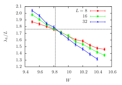


Appendix D Remarks on the choice of boundary conditions: determining the critical point
In the actual calculation finite-size effects can be a serious problem for determining the critical point. To reduce the size effects it is sometimes useful to apply an open boundary condition, e.g., in the case of insulator-insulator transitions, and in the regime of weak disorder.
D.1 Periodic boundary condition
Two panels of Fig. 10 represent a typical example of our size-scaling analysis. The left panel shows the localization length (divided by ) as a function of disorder strength as varying the size of the system. To perform numerical estimate of the localization length we make the system in the form of a long, quasi-one dimensional tube of length and circumference (periodic boundary condition is applied in the circumferential direction). Here, the Rashba SOC is finite (), and the phase diagram shows a metallic region between the two – one topological, the other ordinary – insulating phases (the system belongs to the symplectic symmetry class). Furthermore, in the range of relevant in these plots, the system undergoes a quantum phase transition from a metal to an ordinary insulator. This appears, in the left panel of Fig. 10, as the change of the size-dependence of from an increasing to a decreasing behavior, with a size-independent critical point in the middle, located roughly around . More precise determination of the critical point needs, however, single-parameter scaling analysis as shown in the right panel of Fig. 10, due to a non-negligible finite-size effect. Dashed lines in the left panel indicate the position of such a critical point: , determined by the size-scaling.
D.2 Open boundary condition for the insulator-insulator transition
Next we consider the case of absent Rashba SOC: , i.e., the system belongs to the unitary class. In this case, only direct transitions between the two distinct topological insulators are expected; no metallic phase appears in between. This is problematic to our numerical analyses, since fitting the data to identify a critical point is much more difficult between two insulating phases. Imagine that on both sides of the scale invariant critical point is a decreasing function of the size as far as the system bears no surface states. To overcome this difficulty, we adopted, here in FIG. 11, an open boundary condition, since then the system can support a pair of gapless edge states in the quantum spin Hall phase, i.e., it becomes a metal-insulator transition. Fitting data to determine a critical point is much easier in the vicinity of a metal-insulator transition than in insulator-insulator transitions. [55, 45] The left panel of FIG. 11 demonstrates determination of such a transition from a one-dimensional metal to an ordinary insulator (, ).
One might notice, however, presence of a stronger finite-size effect here compared to the case of (FIG. 10, left panel). Here, the existence of a scale invariant point is no longer evident, and besides, apparent location of the focal point is much deviated from that of the critical point: (indicated by dashed lines) determined by the single-parameter scaling (fitting shown in the right panel). Existence of such a stronger finite-size effect is a disadvantage of an open boundary condition. [55, 45]
D.3 Open boundary condition for the weakly disordered regime
Use of an open boundary condition has another area of utility. In the weak disorder region, the localization length becomes large. The larger becomes, the larger system one needs to consider to perform estimates of the localization length. Use of an open boundary condition is useful for such a case, since the typical length scale of the system, i.e., the critical value of the localization length is smaller in system with an open boundary. This is, on the other hand, applicable only for a metal to an ordinary insulator transition; e.g., in FIG. 4 only the phase boundary between OI and metal could be determined in this way. This is because a metal-TI transition in an open boundary condition becomes metal-metal transition, which is also difficult to determine the critical point as insulator-insulator transition.
Appendix E Symmetry of the phase diagram
Let us finally comment on the symmetry of the phase diagrams shown in Figs. 3–5 with respect to . Let us define the local gauge transformation as
| (36) |
which corresponds to -shift in the momentum space, where is a position on a square lattice. With replacing , Hamiltonian Eq. (1) has symmetry as
| (37) |
Note that although disorder potential Eq. (7) is not microscopically invariant for the above transformation, disorder-averaged quantities such as a Green’s function become invariant. Consequently, the phase diagram becomes symmetric with respect to .
References
- [1] C. L. Kane and E. J. Mele, Phys. Rev. Lett. 95, 146802 (2005a).
- [2] M. Z. Hasan and C. L. Kane, Rev. Mod. Phys. 82, 3045 (2010).
- [3] X.-L. Qi and S.-C. Zhang, Rev. Mod. Phys. 83, 1057 (2011).
- [4] B. Yan and S.-C. Zhang, Rep. Prog. Phys. 75, 096501 (2012).
- [5] C. L. Kane and E. J. Mele, Phys. Rev. Lett. 95, 226801 (2005b).
- [6] M. Konig, S. Wiedmann, C. Brune, A. Roth, H. Buhmann, L. W. Molenkamp, X.-L. Qi, and S.-C. Zhang, Science 318, 766 (2007).
- [7] B. A. Bernevig, T. L. Hughes, and S.-C. Zhang, Science 314, 1757 (2006).
- [8] C. Liu, T. L. Hughes, X.-L. Qi, K. Wang, and S.-C. Zhang, Phys. Rev. Lett. 100, 236601 (2008).
- [9] I. Knez, R. R. Du, and G. Sullivan, Phys. Rev. B 81, 201301 (2010).
- [10] I. Knez, R.-R. Du, and G. Sullivan, Phys. Rev. Lett. 107, 136603 (2011).
- [11] I. Knez and R.-R. Du, Front. Phys. 7, 200 (2012).
- [12] F. J. Dyson, J. Math. Phys. 3, 140 (1962).
- [13] A. Altland and M. R. Zirnbauer, Phys. Rev. B 55, 1142 (1997).
- [14] M. R. Zirnbauer, J. Math. Phys. 37, 4986 (1996).
- [15] A. P. Schnyder, S. Ryu, A. Furusaki, and A. W. W. Ludwig, Phys. Rev. B 78, 195125 (2008).
- [16] A. Kitaev, AIP Conference Proceedings 1134, 22 (2009).
- [17] A. P. Schnyder, S. Ryu, A. Furusaki, and A. W. W. Ludwig, AIP Conference Proceedings 1134, 10 (2009).
- [18] S. Ryu, A. P. Schnyder, A. Furusaki, and A. W. W. Ludwig, New Journal of Physics 12, 065010 (2010).
- [19] M. Onoda, Y. Avishai, and N. Nagaosa, Phys. Rev. Lett. 98, 076802 (2007).
- [20] H. Obuse, A. Furusaki, S. Ryu, and C. Mudry, Phys. Rev. B 76, 075301 (2007).
- [21] H. Obuse, A. Furusaki, S. Ryu, and C. Mudry, Phys. Rev. B 78, 115301 (2008).
- [22] K. Kobayashi, T. Ohtsuki, and K. Slevin, Int. J. Mod. Phys. Conf. Ser. 11, 114 (2012).
- [23] Y. Asada, K. Slevin, and T. Ohtsuki, Phys. Rev. Lett. 89, 256601 (2002).
- [24] R. S. K. Mong, J. H. Bardarson, and J. E. Moore, Phys. Rev. Lett. 108, 076804 (2012).
- [25] K. Kobayashi, T. Ohtsuki, and K.-I. Imura, arXiv:1210.4656 .
- [26] L. Fu and C. L. Kane, arXiv:1208.3442 .
- [27] K.-I. Imura, Y. Kuramoto, and K. Nomura, EPL (Europhysics Letters) 89, 17009 (2010a).
- [28] K.-I. Imura, Y. Kuramoto, and K. Nomura, Phys. Rev. B 80, 085119 (2009).
- [29] J. Li, R.-L. Chu, J. K. Jain, and S.-Q. Shen, Phys. Rev. Lett. 102, 136806 (2009).
- [30] C. W. Groth, M. Wimmer, A. R. Akhmerov, J. Tworzydło, and C. W. J. Beenakker, Phys. Rev. Lett. 103, 196805 (2009).
- [31] A. Yamakage, K. Nomura, K.-I. Imura, and Y. Kuramoto, J. Phys. Soc. Jpn. 80, 053703 (2011).
- [32] E. Prodan, J. Phys. A 44, 113001 (2011a).
- [33] E. Prodan, Phys. Rev. B 83, 195119 (2011b).
- [34] D. Xu, J. Qi, J. Liu, V. Sacksteder, X. C. Xie, and H. Jiang, Phys. Rev. B 85, 195140 (2012).
- [35] Y.-Y. Zhang, R.-L. Chu, F.-C. Zhang, and S.-Q. Shen, Phys. Rev. B 85, 035107 (2012).
- [36] H.-M. Guo, G. Rosenberg, G. Refael, and M. Franz, Phys. Rev. Lett. 105, 216601 (2010).
- [37] P. Goswami and S. Chakravarty, Phys. Rev. Lett. 107, 196803 (2011).
- [38] S. Ryu and K. Nomura, Phys. Rev. B 85, 155138 (2012).
- [39] S. Mao and Y. Kuramoto, Phys. Rev. B 83, 085114 (2011).
- [40] E. Abrahams, P. W. Anderson, D. C. Licciardello, and T. V. Ramakrishnan, Phys. Rev. Lett. 42, 673 (1979).
- [41] A. MacKinnon and B. Kramer, Phys. Rev. Lett. 47, 1546 (1981).
- [42] A. MacKinnon and B. Kramer, Z. Phys. B 53, 1 (1983).
- [43] B. Kramer and A. MacKinnon, Rep. Prog. Phys. 56, 1469 (1993).
- [44] P. Markoš, Acta Phys. Slov. 56, 561 (2006).
- [45] H. Obuse, A. R. Subramaniam, A. Furusaki, I. A. Gruzberg, and A. W. W. Ludwig, Phys. Rev. B 82, 035309 (2010).
- [46] E. P. L. van Nieuwenburg, J. M. Edge, J. P. Dahlhaus, J. Tworzydło, and C. W. J. Beenakker, Phys. Rev. B 85, 165131 (2012).
- [47] S. Hikami, A. I. Larkin, and Y. Nagaoka, Prog. Theor. Phys. 63, 707 (1980).
- [48] T. Ando, Phys. Rev. B 40, 5325 (1989).
- [49] V. Juričić, A. Mesaros, R.-J. Slager, and J. Zaanen, Phys. Rev. Lett. 108, 106403 (2012).
- [50] A. Matsumoto, Graduation Thesis, Faculty of Engineering, Hiroshima University, March 2012.
- [51] R. Shindou and S. Murakami, Phys. Rev. B 79, 045321 (2009).
- [52] D. G. Rothe, R. W. Reinthaler, C.-X. Liu, L. W. Molenkamp, S.-C. Zhang, and E. M. Hankiewicz, New J. Phys. 12, 065012 (2010).
- [53] L. Fu and C. L. Kane, Phys. Rev. B 74, 195312 (2006).
- [54] K.-I. Imura, A. Yamakage, S. Mao, A. Hotta, and Y. Kuramoto, Phys. Rev. B 82, 085118 (2010b).
- [55] T. Ohtsuki, K. Slevin, and T. Kawarabayashi, Ann. Phys. 8, 655 (1999).