Spin-Valley Optical Selection Rule and Strong Circular Dichroism in Silicene
Abstract
Silicene (a monolayer of silicon atoms) is a topological insulator, which undergoes a topological phase transition to a band insulator under an external electric field. The spin polarization is unique and opposite at the K and K’ points due to the spin-orbit coupling. Accordingly, silicene exhibits a strong circular dichroism with respect to optical absorption, obeying a certain spin-valley selection rule. It is remarkable that this selection rule is drastically different between these two types of insulators owing to a band inversion taking place at the phase transition point. Hence we can tell experimentally whether silicene is in the topological or band insulator phase by circular dichroism. Furthermore the selection rule enables us to excite electrons with definite spin and valley indices by optical absorption. Photo-induced current is spin polarized, where the spin direction is different between the topological and band insulators. It is useful for future spintronics applications.
Introduction: Silicene consists of a honeycomb lattice of silicon atoms with buckled sublattices made of A sites and B sites. The states near the Fermi energy are orbitals residing near the K and K’ points at opposite corners of the hexagonal Brillouin zone. Silicene has recently been synthesized[1, 2, 3] and attracted much attention[4, 5, 6, 7]. The low-energy dynamics in the K and K’ valleys is described by the Dirac theory as in graphene. However, Dirac electrons are massive due to a relatively large spin-orbit (SO) gap of meV in silicene. It is remarkable that the mass can be controlled[6] by applying the electric field perpendicular to the silicene sheet.
A novel feature is that silicene is a topological insulator[5], which is characterized by a full insulating gap in the bulk and helical gapless edges[8, 9]. It undergoes a topological phase transition from a topological insulator to a band insulator as increases and crosses the critical field , as has been shown by examining numerically the emergence of the helical zero energy modes in silicene nanoribbons[6] and also by calculating the topological numbers[10]. It is an intriguing problem how to detect experimentally whether an insulator is topological or not just by the bulk property.

The interaction of light with matter depends on the polarization of the photons in general. When the response of a system to the left- and right-handed circularly polarized light is different, the phenomenon is referred to as circular dichroism. The circular dichroism has been shown to be essential to analyze the valley-dependent interplay of electrons in graphene[18, 11] as well as in monolayer dichalcogenides[12, 17].
In this paper, we investigate optical absorptions in silicene. The crucial property is the spin polarization is unique and opposite at the K and K’ points due to the SO coupling for . Hence silicene exhibits a strong circular dichroism, where the optical absorption of circularly polarized light strongly depends on the spin and valley. Furthermore, the optical selection rules are entirely different between a topological insulator and a band insulator, as enables us to tell whether silicene is in the topological or band insulator phase. The difference originates in a band inversion taking place at the phase transition point. It is remarkable that we can detect a topological phase transition by the change of circular dichroism as crosses the critical field . It is also remarkable that, by irradiating right-handed circularly polarized light, for instance, we can selectively excite up spin at the K point. By applying an in-plane electric field, photo-exicited spin-polarized charges can be extracted. We can determine whether the system is topological or band insulator by detecting the spin direction of the photo-induced current.
Low-Energy Dirac Theory: We take a silicene sheet on the -plane, and apply the electric field perpendicular to the plane. Due to the buckled structure the two sublattice planes are separated by a distance, which we denote by with Å , as illustrated in Fig.1. It generates a staggered sublattice potential between silicon atoms at A sites and B sites.
We analyze the physics of electrons near the Fermi energy, which is described by Dirac electrons near the K and K’ points. We also call them the Kξ points with . The effective Dirac Hamiltonian in the momentum space reads[7]
| (1) |
where and are the Pauli matrices of the spin and the sublattice pseudospin, respectively. We explain each term. The first term arises from the nearest-neighbor hopping, where m/s is the Fermi velocity with the transfer energy eV and the lattice constant Å. The second term represents the effective SO coupling[13, 14] with meV. The third term represents the staggered sublattice potential[6] in electric field . The forth term represents the second Rashba SO coupling with meV associated with the next-nearest neighbor hopping term[14]. The fifth term represents the first Rashba SO coupling associated with the nearest neighbor hopping, which is induced by external electric field[15, 16]. It satisfies and becomes of the order of eV at the electric field meVÅ-1. Its effect is negligible as far as we have checked. Although we include all terms in numerical calculations, in order to simplify the formulas and to make the physical picture clear, we set in all analytic formulas.

There are four bands in the energy spectrum (Fig.2). The band gap is located at the K and K’ points. At these points the energy is given by
| (2) |
with the spin and the sublattice pseudospin . They are good quantum numbers at the K and K’ points. The spin is an almost good quantum number even away from the K and K’ points because is a small quantity. On the other hand, the pseudospin is strongly broken away from the K and K’ points for .
The gap is given by with
| (3) |
where is the spin-chirality. It is given by when the spin is a good quantum number. As increases, the gap decreases linearly, and closes at the critical point with
| (4) |
and then increases linearly. Silicene is a semimetal due to gapless modes at , while it is an insulator for .
Optical properties: We explore optical interband transitions from the state in the valence band to the state in the conduction band. There are four transitions, which we label as , , and , as depicted in Fig.3. We call as the fundamental transition.

We consider a beam of circularly polarized light irradiated onto the silicene sheet. The corresponding electromagnetic potential is given by
| (5) |
The electromagnetic potential is introduced into the Hamiltonian (1) by way of the minimal substitution, that is, replacing the momentum with the covariant momentum . The resultant Hamiltonian simply reads
| (6) |
with (1) and
| (7) |
since the Dirac Hamiltonian is linear in the momentum. It is notable that the formula does not contain the SO coupling . We conclude from this formula that the kinetic term () induces an interband transition between electrons carrying the same spin while the Rashba term () induces an interband transition between electrons carrying the opposite spins.

The coupling strength with optical fields of the right() or left() circular polarization is given by . They are written in terms of the ladder operator of spins and pseudospins.
| (8) | |||||
| (9) |
where and .
The matrix element between the initial state and the final state in the photoemission process is given by
| (10) |
where is the free electron mass. Here, is called the optical absorption. There exist the relations,
| (11) |
reflecting the time-reversal symmetry. The right-handed circular polarization at the K point and the left-handed circular polarization at the K’ point are equal.
The wave functions and are obtained explicitly by diagonalizing the Hamiltonian (1). We have calculated numerically the optical absorption as a function of near the K and K’ points, which we display in Fig.4.
Let us investigate the optical absorption at in detail, since we can obtain a clear physical picture at the K and K’ points with the aid of analytical formulas. The Hamiltonian (1) is diagonal at the K and K’ points with the eigenvalues given by (2) and the eigenfunctions given by and so on. For , the order of the energy level is
| (12) |
for the topological insulator, and
| (13) |
for the band insulator. It is to be emphasized that the two bands near the Fermi level are inverted between the topological and band insulators, since the pseudospin is flipped as exceeds the critical point .
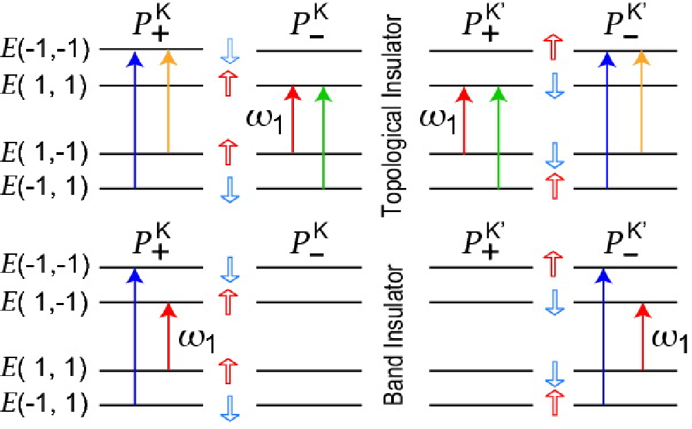
The band inversion leads to a different circular dichroism. This is because the operator is not Hermitian: describes an optical absorption process, while describes an optical emission process. Furthermore, an optical absorption occurs only when the energy of the initial state is lower than that of the final state. Thus the optical absorption obeys a strong spin-valley coupled selection rule (Fig.5). In conclusion, the fundamental optical absorption (indicated by red arrow) is different whether the system is a topological insulator or a band insulator. For example, the right-circular polarized light at the K point is absorbed only when the system is a band insulator, while the left-circular polarized light at the K point is absorbed only when the system is a topological insulator. Furthermore the spin-flipped interband transitions occur only when the system is a topological insulator.
We show the optical absorption for various electric field in Fig.6. If we neglect the Rashba terms () we are able to obtain an analytic formula for the transitions and near the Kξ point,
| (14) |
where for and for . When the electric field is critical, , where , the optical absorption of the fundamental transition becomes a constant,
| (15) |
which is common to the K and K’ valleys. This property holds as it is even for , as seen in Fig.6.

The -resolved optical polarization is given by
| (16) |
This quantity is the difference between the absorption of the left- and right-handed lights (), normalized by the total absorption, around the Kξ point. We show the optical polarization for the topological and band insulators in Fig.7. We find that all optical polarizations are perfectly polarized at the K and K’ points (). Namely, the selection rule holds exactly at the K and K’ points, where . Then, decreases to as increases. It is to be emphasized that the optical polarization of the fundamental interband transition is opposite whether the system is a topological insulator or a band insulator.

By neglecting the Rashba term (), we obtain an analytic formula of the optical polarization for the transitions and ,
| (17) |
The optical polarization changes the sign at the topological phase transition , since changes the sign. This property holds as it is even for , as seen in Fig.7.
In this paper we have analyzed optical absorption in silicene. We have shown that silicene exhibits a strong circular dichroism obeying the spin-valley selection rule (Fig.5). The response is opposite whether silicene is a topological or band insulator. Indeed, in the topological (band) insulator phase, the optical field with the right-handed circular polarization excites only up-spin (down-spin) electrons in the K valley, while the one with the left-handed circular polarization excites only down-spin (up-spin) electrons in the K’ valley, as far as the fundamental transition concerns. Now, we are able to generate a longitudinal charge current with a definite spin by applying an in-plane electric field. By measuring the spin direction we can tell if silicene is a topological or band insulator.
I am very much grateful to N. Nagaosa for many helpful discussions on the subject. This work was supported in part by Grants-in-Aid for Scientific Research from the Ministry of Education, Science, Sports and Culture No. 22740196.
References
- [1] P. Vogt, , P. De Padova, C. Quaresima, J. A., E. Frantzeskakis, M. C. Asensio, A. Resta, B. Ealet and G. L. Lay, Phys. Rev. Lett. 108, 155501 (2012).
- [2] C.-L. Lin, R. Arafune, K. Kawahara, N. Tsukahara, E. Minamitani, Y. Kim, N. Takagi, M. Kawai, Appl. Phys. Express 5, Art No. 045802 (2012) .
- [3] A. Fleurence, R. Friedlein, T. Ozaki, H. Kawai, Y. Wang, and Y. Yamada-Takamura, Phys. Rev. Lett. 108, 245501 (2012).
- [4] S. Cahangirov, M. Topsakal, E. Aktürk,1 H. Sahin, and S. Ciraci, Phys. Rev. Lett. 102, 236804 (2009).
- [5] C.-C. Liu, W. Feng, and Y. Yao, Phys. Rev. Lett. 107, 076802 (2011).
- [6] M. Ezawa, New J. Phys. 14, 033003 (2012).
- [7] M. Ezawa, cond-mat/arXiv:1203.0705 (to be published in Phys. Rev. Lett.).
- [8] M.Z Hasan and C. Kane, Rev. Mod. Phys. 82, 3045 (2010).
- [9] X.-L. Qi and S.-C. Zhang, Rev. Mod. Phys. 83, 1057 (2011).
- [10] M. Ezawa, cond-mat/arXiv:1205.6541.
- [11] W. Yao, D. Xiao, and Q. Niu, Phys. Rev. B 77, 235406 (2008).
- [12] D. Xiao, G.-B. Liu, W. Feng, X. Xu, and W. Yao, Phys. Rev. Lett. 108, 196802 (2012).
- [13] C. L. Kane and E. J. Mele, Phys. Rev. Lett. 95, 226801 (2005); ibid 95, 146802 (2005).
- [14] C.-C. Liu, H. Jiang, and Y. Yao, Phys. Rev. B, 84, 195430 (2011).
- [15] H. Min, J. E. Hill, N. A. Sinitsyn, B. R. Sahu, L. Kleinman, and A. H. MacDonald, Phys. Rev. B 74, 165310 (2006).
- [16] W.K. Tse, Z. Qiao, Y. Yao, A. H. MacDonald, and Q. Niu, Phys. Rev. B 83, 155447 (2011).
- [17] T. Cao, J. Feng, J. Shi, Q. Niu, E. Wang, cond-mat/arXiv:1112.4013.
- [18] D. Xiao, W. Yao, and Q. Niu, Phys. Rev. Lett. 99, 236809 (2007).