Observation of spin-selective tunneling in SiGe nanocrystals
Abstract
Spin-selective tunneling of holes in SiGe nanocrystals contacted by normal-metal leads is reported. The spin selectivity arises from an interplay of the orbital effect of the magnetic field with the strong spin-orbit interaction present in the valence band of the semiconductor. We demonstrate both experimentally and theoretically that spin-selective tunneling in semiconductor nanostructures can be achieved without the use of ferromagnetic contacts. The reported effect, which relies on mixing the light and heavy holes, should be observable in a broad class of quantum-dot systems formed in semiconductors with a degenerate valence band.
pacs
73.23.Hk; 71.70.Ej; 73.63.KvThe spin-orbit interaction (SOI) has become of central interest in the past years [1], because it enables an all-electrical manipulation of the spin. In the field of spin qubits, one of us [2] suggested the electrical control of localized spins by means of the electric-dipole spin resonance, and this scheme has been successfully used for spin rotations of electrons in quantum dots (QDs) [3, 4]. Already much earlier, Datta and Das [5] proposed a semiconductor transistor that would operate through a gate-controlled spin precession, mediated by the SOI. In this type of spin transistor, spin-polarized electrons are injected into the semiconductor from a ferromagnetic (FM) contact. The realization of an efficient spin injection has proven to be a difficult task [6, 7]. Only recently, high spin-injection efficiencies were reported for FM contacts to semiconductors [8, 9, 10]. In nanostructures, however, experimental evidence of spin injection is not as strong and clear [11, 12, 13, 14, 15]. Here we show that the SOI in the valence band, quantified by the spin-orbital splitting , provides an alternative way to obtain spin-selective tunneling without requiring FM electrodes.
At cryogenic temperatures, transport through QDs is dominated by the Coulomb blockade (CB) effect. In the CB regime, single-hole transport is suppressed and electrical conduction is due to second-order cotunneling (CT) processes [16]. We consider here the case of a QD with an odd number of holes and a spin-doublet ground state. A magnetic field, , lifts the spin degeneracy by the Zeeman energy , where and are the hole g-factor and Bohr magneton, respectively. Once the bias voltage across the QD exceeds the Zeeman energy, , the inelastic CT processes can flip the QD spin, leaving the QD in the excited spin state; hereinafter is the elementary charge (). The onset of spin-flip inelastic CT manifests itself as a step in the differential conductance, , at [17].


Our measurements reveal a pronounced asymmetry in the step height of with respect to the polarity of , as recently predicted by Paaske et al. [18], in a model with a rather generic form of the SOI interaction. The asymmetry is found to depend on the magnitude and direction of . Our results are consistent with an explanation based on the Luttinger Hamiltonian for the valence band of the semiconductor. The spin selectivity of tunneling arises from an interplay of the complex structure of the valence band with the orbital effect of the magnetic field. At , the time-reversal symmetry ensures that the two states forming the Kramers doublet in the QD are indistinguishable and the spin selectivity of tunneling vanishes.


It is interesting to note that the transport characteristics of a QD with SOI coupled to normal leads are similar to those of a QD without SOI coupled to FM leads. We illustrate this similarity in Fig. 1, where we consider the simplest case, in which the Zeeman interaction and the two spin-dependent tunnel contacts have collinear quantization directions.
We have studied the low-temperature magneto-transport properties of individual SiGe self-assembled QDs with a base diameter nm and a height nm. The hole motion is strongly quantized along the growth direction . A schematic of a typical QD contacted with Al electrodes is shown in Fig. 2(a). For such QDs, the hole wave function is generally composed of both heavy holes (HHs) and light holes (LHs). Due to the confinement and compressive strain, the degeneracy between the HH and LH branches, present in bulk at the -point, is lifted. The HHs become energetically favorable. In Fig. 2(b), we illustrate the interaction between a HH and a LH branch in the two-dimensional (2D) case. The split-off band is far away in energy due to a large . HHs and LHs are states of angular momentum with projections and , respectively, see Appendix B. We remark that, contrary to the HH states, the LH states cannot be factorized into a product of spin and orbital components.
The stability diagram, , of a QD device is shown in the inset of Fig. 2(c). The diamond-shape region delimited by dashed lines highlights the CB regime for an odd number of confined holes. While is generally suppressed within this CB diamond, a resonance can be identified at , providing a clear signature of a spin- Kondo effect [20]. At finite , this resonance is split by the Zeeman effect as shown in Figs. 2 (c) and (d) for perpendicular and parallel , respectively (all traces were taken at the same ).

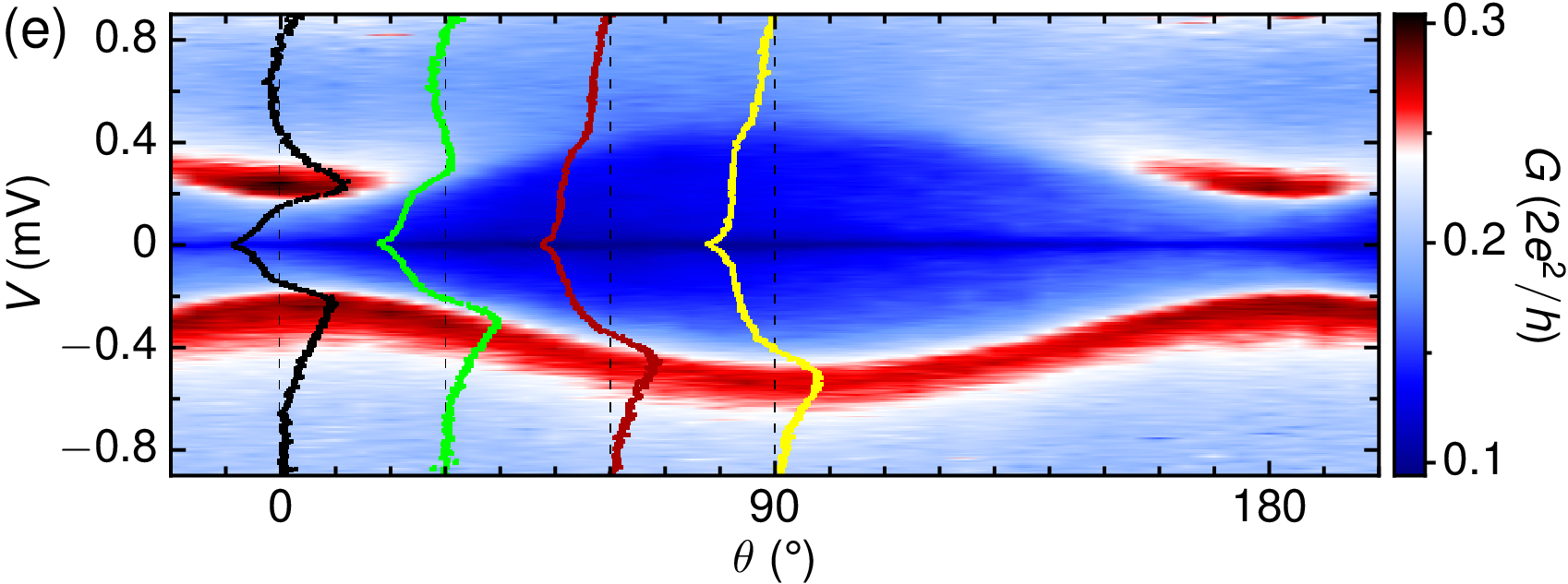
For perpendicular [Fig. 2(c)], the splitting of the Kondo peak is clearly asymmetric with respect to a sign change in . The asymmetry in arises at the onset of spin-flip inelastic CT (i.e. for ). For parallel , however, the asymmetry is practically absent [Fig. 2(d)]. To further investigate this anisotropy, a sequence of traces was taken while rotating a field in a plane perpendicular to the substrate. The resulting data, , are shown in Fig. 2(e), with being the angle between the field and the substrate plane. Along with a variation in the Zeeman splitting of the Kondo peak, caused by the -dependent hole g-factor [19], the asymmetry becomes progressively more pronounced when going from (or ) towards .
The asymmetry observed in can be quantified by , where . The detailed dependence, extracted from Fig. 2(e), is shown in Fig. 3(a). for (or ) and it increases monotonically up to for approaching . The same qualitative behavior was observed in a second device, which did not display Kondo effect, see Appendix A. The asymmetry reaches at for that device. We remark that, although the first device shows larger conductance due to the Kondo effect, the asymmetry in both devices is a consequence of spin-dependent tunnel rates.
In order to explain the microscopic origin of the measured effect, we represent the Luttinger Hamiltonian [21] as a block matrix in the basis of HH () and LH () states,
| (1) |
In the blocks and , we discard all terms that vanish in the 2D limit (), whereas in the blocks and , we keep only the leading-order in terms. A systematic expansion around the 2D limit is outlined in the Appendix B. The blocks and assume a familiar form
| (2) | |||||
where the axes , , and point along the main crystallographic directions, with being the direction of the strongest quantization. After the expansion around the 2D limit, the kinetic momentum operators and contain only the component , whereas is independent of . In Eq. (2) and below, , , , , and denote the Luttinger parameters [21] and denotes the bare electron mass. The Pauli matrices represent the remaining pseudo-spin degree of freedom in each block. We choose the following pseudo-spin basis [30]:
| (3) |
In the -frame, the tensors of the g-factor are diagonal: and , where we neglected, for simplicity, the terms proportional to the smallest Luttinger parameter . The minus sign in is due to our basis choice in Eq. (3). In Eq. (2), we included an in-plane confining potential . The motion along is confined to an infinitely-deep square well, with different offsets, and , due to strain.
The blocks and are given by
| (4) |
These blocks intermix HHs and LHs, such that the wave function of the hole in a given QD state assumes the general form . In terms of the true-spin states, such a wave function consists of a superposition of the spin-up () and spin-down () states entangled with the orbital degrees of freedom:
| (5) |
where and denote the components of the Kramers doublet in the QD. Focusing on the first HH subband, we obtain by perturbation theory:
| (6) | |||||
and similar expressions for and , obtained from Eq. (6) by replacing , , and . In our notation, and . The Bloch amplitudes , , and describe the valence band in the absence of SOI. In blocks and , the motion along separates; we denote the corresponding eigenenergies and eigenfunctions by and , respectively.
The tunneling amplitudes are found as
| (7) |
where is the coupling strength between Bloch amplitude and the lead, and are the projections of the QD eigenstates , see Eq. (5), onto the product state of Bloch amplitude and spinor . The tunneling amplitudes in Eq. (7) depend on the point of tunneling, , the component of the true spin in the lead, , and the component of the Kramers doublet on the dot, . We remark that , , and appear in Eq. (7) as phenomenological parameters. They depend on the details of the metal-semiconductor interface and cannot be determined within the -theory used here. We find
| (8) |
where and are obtained from Eq. (6) by replacing and .

The spin selectivity of the tunneling is best seen in the matrix of the tunnel rates, . With (case of non-FM leads) we find, up to a common factor,
| (9) |
At , time-reversal symmetry requires that
| (10) |
leading to and in Eq. (9).
At , however, the orbital effect of the -field modifies the functions and , such that the relations in Eq. (10) are no longer satisfied. In general, the matrix has nonzero off-diagonal elements. Since it is a hermitian matrix, there exists a direction in space, , such that an rotation of the Kramers doublet by an angle makes the rate matrix diagonal, , with . To quantify the spin selectivity of the tunneling, we define
| (11) |
In respect to transport, is analogous to the polarization vector of the FM. Indeed, the maximum of spin selectivity in tunneling from a FM is achieved when the FM is a half-metal, e.g., and . This extreme case corresponds to and can be approached in our case by increasing .
In order to illustrate the origin of the spin selectivity, we focus on the special case: and and refer to this tunneling model as the -model. In the -model, vector is parallel to the -axis. Tunneling to the hole states is possible only due to the admixture of the LH subbands. Furthermore, in this model, the spin selectivity is determined by the fact that and , whereas . Using this information in Eqs. (9) and (11), we specify to the Fock-Darwin states [23]. Therefore, we assume that in Eq. (2) is given by , where is the effective mass for in-plane motion, is the oscillator frequency of the harmonic potential, and . For the first two states ( and ), we obtain
| (12) |
where , and . For these states, depends on but not on , see Fig. 4(a). For , the contacts will exhibit spin-dependent tunnel rates with the same polarization value regardless of the point-tunneling position. In such a case, no asymmetry in the inelastic CT is expected.
The situation changes starting from and , where
| (13) |
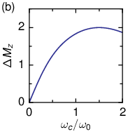
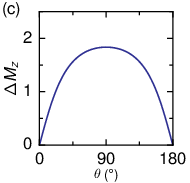
with . Now depends both on and on , see Fig. 4(a). The spin polarization of two contacts positioned arbitrarily on a QD may differ significantly from each other, see, e.g., points and in Fig. 4(a). The asymmetry in the inelastic CT is related to . increases with [Fig. 4 (b)], displaying at the same time strong dependence on the -field direction [Fig. 4 (c)], in good qualitative agreement with the results in Fig. 3.
The described joint effect of SOI and Zeeman splitting explains our experimental findings. In addition, it opens the door to an original scheme for measuring Rabi spin oscillations in hole confinement QDs. Let us consider a spin-1/2 QD in the CB regime under a perpendicular of the order of a few T. In such a case, a transport characteristic of the type shown in Fig. 2(c) is to be expected. For , no current flows through the QD. Yet we suggest that a finite current could be generated by a resonant rf field (at frequency ) capable of inducing coherent oscillations between the Zeeman-split states of the QD. In fact, as the excited state becomes populated it can decay to the ground state by an inelastic CT process—a hole tunnels out of the QD from the state being replaced by another hole tunneling into the state. Because and states have tunnel couplings with opposite asymmetries, in a configuration such as the one depicted in Fig. 1(b) the most favorable CT relaxation process would involve the transfer of a hole from the right to the left contact. Hence a net dc current could be driven by a continuous resonant irradiation. In addition, combining rf bursts with syncronized pulses may enable the coherent control of the QD pseudo-spin states. In this scheme, well-defined pseudo-spin rotations would be performed in the deep CB regime (i.e. during a negative pulse), whereas pseudo-spin read-out would take place in the CT regime.
We acknowledge J. Paaske for helpful discussions and A. Rastelli and H. von Kaenel for providing the STM image used in Fig. 1(a). The work was supported by the Agence Nationale de la Recherche (through the ACCESS and COHESION projects), US DOE Contract No. DE-FG02-08ER46482 (Yale), and the Nanosciences Foundation at Grenoble, France. G.K. acknowledges support from the Deutsche Forschungsgemeinschaft.

Appendix A Second device
Similar asymmetries as the ones described in the main text were observed also for a second device, less strongly coupled to the metallic leads. Figure 5 (a) is a plot of the differential conductance versus the angle of magnetic field and the bias voltage for a fixed value of 3 T. Differently to the first device the minimum g-factor is not observed for a parallel magnetic field but there is a shift by about 15-20 degrees. Some characteristic traces of G vs taken at 20 (blue), 45 (red) and 90 (black) degrees are shown in Fig. 5 (b). Interestingly, the position of the minimum g-factor coincides with the case for which no asymmetry is appearing (15-20 degrees). We believe that both observations are because the 2D plane of the wave function is not parallel to the substrate.
The asymmetry follows the same trends as were observed in the first device. It is almost zero for 15-20 degrees (the position of the minimum ) and it obtains values of about 0.35-0.4 at large out of plane angles of the magnetic field [Fig. 5 (c)]. The difference in the value of A for positive and negative magnetic fields is attributed again to the different angle the 2D hole wavefunction plane forms with the magnetic field. Finally, Fig. 5 (d), verifies that the asymmetry increases with .
We remark that in the absence of misalignment the asymmetry obeys the relation
| (14) |
which holds within the experimental accuracy for the device described in the main text. Equation (14) can be understood as follows. On the one hand, the spin-selective part of is proportional to the orbital and therefore it changes sign when flipping the direction of the magnetic field. On the other hand, the Zeeman energy is also changing sign when flipping the direction of the magnetic field, swapping thus the roles of the ground and the excited state. As a result, the measured cotunneling asymmetry does not change sign when changing .
Appendix B Expansion around the 2D limit
Our starting point is the Luttinger Hamiltonian [24],
| (15) |
where is the mass of the electron in vacuum, , , , , and are the Luttinger parameters, is the momentum of the band electron,
| (16) |
with being the vector potential due to the magnetic field, the elementary charge (), and the speed of light. Further, denotes the symmetrized product, e.g.
| (17) |
and are matrices representing the spin in a basis of choice. We choose the basis [25]
| (18) |
where
| (19) |
Here, the Bloch amplitudes , , and are chosen to be real. They belong to the representation of the group and transform under the group operations as , , and [26, 27, 28]. The basis functions , , and form a subspace that is equivalent to the space of the angular momentum [24]. The states in Eq. (19) originate from the addition [29] , where is the electron spin () in the usual basis . The subspace of is shown in Eq. (19), whereas the subspace of is neglected, because it corresponds to the split-off band, i.e. the band that is shifted, due to the spin-orbit interaction, by an amount below the top of the valence band. The Luttinger Hamiltonian describes the very top of the valance band, at energies . In the basis given by Eqs. (18) and (19), the matrices of read [25]
| (20) |
| (21) |
| (22) |
In Eq. (15), the axes , , and are fixed along the main crystallographic directions of the cubic crystal. We choose the axis to point along the growth direction of the nanocrystal, making it the axis of the strongest size quantization. The idea of expanding the Luttinger Hamiltonian around the 2D limit consists in regarding quantities like and as proportional to and , respectively. Here, is the width of the 2D layer (i.e. height of nanocrystal), which is considered to be much smaller than the nanocrystal diameter . On the other hand, quantities like and are regarded as proportional to and , respectively [30]. Before expanding in powers of , it is convenient to represent the Luttinger Hamiltonian in a block form.
We use two projection operators, and , which project on the subspaces of the heavy () and light () holes. In terms of , they are written as
| (23) |
and resolve the unity, , and have the usual properties of projection operators: , , and . The Luttinger Hamiltonian in Eq. (15) can then be written as follows
| (24) | |||||
which makes up a matrix in the -space,
| (25) |
Each element can be represented as a matrix in the space of the pseudo-spin. The blocks on the diagonal read
| (26) | |||||
where the g-factors and are tensors. In the frame , they are diagonal:
| (27) |
and
| (28) |
The off-blocks are related to each other by hermiticity,
| (29) |
For , we have
| (30) | |||||
All we have done so far was to rewrite the Luttinger Hamiltonian in a block form. Next we proceed with the expansion in powers of as explained above.
We allow for gauges of the form
| (31) |
where is a real number expressing the remaining gauge freedom in two dimensions. After taking the 2D limit, we will be able to use a reduced (2D) vector potential, , which is given by
| (32) |
Having in mind such a transition, we pull out the -dependence from and ,
| (33) |
Here, on the right-hand side, and do not depend on anymore, because they are given in terms of the 2D vector potential as
| (34) |
The next step is to substitute Eq. (33) into the Luttinger Hamiltonian and to group the terms according to their order of .
The substitution of Eq. (33) in the blocks and produces linear in and terms which are not multiplied by any Pauli matrix. Such terms can be gauged away after integration over , since they correspond to a constant shift in and . They also admix higher heavy-hole subbands and slightly renormalize the inplane mass, but this admixture, as well as the mass renormalization, vanishes in the limit , because the corresponding perturbation is proportional to . Therefore, we dispense with the new terms generated in and .
We note that, for the blocks and , the transition to 2D is identical to what is usually done for electrons in the conduction band.
For the blocks and , we make the substitution in Eq. (33) and obtain lots of terms. The origin of each term can be traced back through the following intermediate step:
| (35) | |||||
Then, we classify all terms according to their order of .
The leading order is that of and the off-block acquires the following main term
| (36) |
It is important to remark that and contain only the -component of the magnetic field. The transverse components and do not appear in at this order of . On this reason, the component has a larger effect on breaking the time-reversal symmetry than the other two components.
The next order is that of and the off-block acquires the following correction
References
- [1] R. Winkler, Spin-Obit Coupling Effects in Two-Dimensional Electron and Hole Systems (Springer 2003).
- [2] V. N. Golovach, M. Borhani, and D. Loss, Phys. Rev. B 74, 165319 (2006).
- [3] K. C. Nowack, F. H. L. Koppens, Yu. V. Nazarov, and L. M. K. Vandersypen, Science 318, 1430, (2007).
- [4] S. Nadj-Perge, S. M. Frolov, E. P. A. M. Bakkers, and L. P. Kouwenhoven, Nature 468, 1084
- [5] S. Datta, and B. Das, Appl. Phys. Lett. 56, 665 (1990).
- [6] I. Žutić, J. Fabian, and S. Das Sarma , Rev. Mod. Phys. 76, 323 (2004).
- [7] E.I. Rashba, Semicond. Sci. Technol. 23, 114015 (2008).
- [8] H. C. Koo, J. H. Kwon, J. Eom, J. Chang, S. H. Han, and M. Johnson , Science 325, 1515 (2009).
- [9] I. Appelbaum, B. Huang, D. Monsma, Nature 447, 295 (2007).
- [10] C.H. Li, O.M.J. van ´t Erve, and B.T. Jonker, Nature Communications, DOI: 10.1038/ncomms1256, (2011).
- [11] K. Tsukagoshi, B. W. Alphenaar, and H. Ago, Nature 401, 572 (1999).
- [12] S. Sahoo, T. Kontos, J. Furer, C. Hoffman, M. Gräber, A. Cottet, and C. Schönenberger , Nat. Phys. 1, 99 (2005).
- [13] K. Hamaya, M. Kitabatake, K. Shibata, M. Jung, M. Kawamura, S. Ishida, T. Taniyama, K. Hirakawa, Y. Arakawa, and T. Machida, Phys. Rev. B 77, 081302(R) (2008).
- [14] F. A. Zwanenburg, D. W. van der Mast. H. B. Heersche, L. P. Kouwenhoven, and E. P. A. M. Bakkers, Nano Lett. 9, 2704 (2009).
- [15] E.-S. Liu, J. Nah, K. M. Varahramyan, and E. Tutuc, Nano Lett. 10, 3297 (2010).
- [16] S. De Franceschi, S. Sasaki, J. M. Elzerman, W. G. van der Wiel, S. Tarucha, and L. P. Kouwenhoven, Phys. Rev. Lett. 86, 878 (2001).
- [17] A. Kogan, S. Amasha, D. Goldhaber-Gordon, G. Granger, M. A. Kastner, and Hadas Shtrikman, Phys. Rev. Lett. 93, 166602 (2004).
- [18] J. Paaske, A. Andersen, and K. Flensberg, Phys. Rev. B 82, 081309(R) (2010).
- [19] G. Katsaros, P. Spathis, M. Stoffel, F. Fournel, M. Mongillo, V. Bouchiat, F. Lefloch, A. Rastelli, O. G. Schmidt, De Franceschi S., Nature nanotechnology 5, 458, (2010).
- [20] D. Goldhaber-Gordon, H. Shtrikman, D. Mahalu, D. Abusch-Magder, U. Meirav, M. A. Kastner, Nature 391, 156-159 (1998).
- [21] See Eq. (45) in J.M. Luttinger, Phys. Rev. 102, 1030 (1956).
- [22] The advantage of this choice is that the pseudo-spin transforms under the time reversal as a spin , i.e. and .
- [23] V. Fock, Z. Phys. 47, 446 (1928); C.G. Darwin, Proc. Cambridge Philos. Soc., 27, 86 (1930).
- [24] J. M. Luttinger, Phys. Rev. 102, 1030 (1956).
- [25] V.N. Abakumov, V.I. Perel, and I.N. Yassievich, Nonradiative Recombination in Semiconductors, (North-Holland, 1991).
- [26] G. Dresselhaus, A.F. Kip, and C. Kittel, Phys. Rev. 98, 368 (1955).
- [27] M. Cardona and F.H. Pollak, Phys. Rev. 142, 530 (1966).
- [28] P.Y. Yu, M. Cardona, Fundamentals of Semiconductors: Physics and Materials Properties, 4th Edition, (Springer-Verlag Berlin Heidelberg, 2010).
- [29] J.M. Luttinger and W. Kohn, Phys. Rev. 97, 869 (1955).
- [30] The same premise is made for and .