Iron-chalcogenide FeSe0.5Te0.5 coated superconducting tapes for high field applications
Abstract
The high upper critical field characteristic of the recently discovered iron-based superconducting chalcogenides opens the possibility of developing a new type of non-oxide high-field superconducting wires. In this work, we utilize a buffered metal template on which we grow a textured FeSe0.5Te0.5 layer, an approach developed originally for high temperature superconducting coated conductors. These tapes carry high critical current densities (1A/cm2) at about 4.2 K under magnetic field as high as 25 T, which are nearly isotropic to the field direction. This demonstrates a very promising future for iron chalcogenides for high field applications at liquid helium temperatures. Flux pinning force analysis indicates a point defect pinning mechanism, creating prospects for a straightforward approach to conductor optimization.
pacs
74.78.-w, 74.70.Ad 74.62.-c, 74.62.Bf,High field applications of superconductors have been dominated by Nb3Sn, a material which allows magnetic fields up to 20 T to be achieved at 4.2 K.[1] However, Nb3Sn wires typically require a post-winding heat-treatment, which is a technically-challenging manufacturing step. Although high temperature superconducting oxides (HTS) offer excellent superconducting properties,[2] their characteristically high anisotropies and brittle textures, in addition to the high manufacturing costs, have limited their applications. The newly-discovered iron-based superconductors are semi-metallic low-anisotropy materials with transition temperatures, ’s, up to 55 K.[3] The combination of extremely high upper critical fields (0) ( 100 T),[4] moderate anisotropies of (1-8),[5] and high irreversibility fields, ,[6] makes this class of superconductors appealing for high field applications. Recently, high critical current densities, ’s, have been reported in Co-doped BaFe2As2[7] and SmFeAs(O,F)[8] systems.
Chalcogenides, which are a sub-class of iron-based superconductors, hold several practical advantages over the pnictides. Although the ’s of chalcogenides are typically below 20 K, they exhibit lower anisotropies 2 with (0)’s approaching 50 T.[9, 10, 11] They also have the simplest structure among the iron-based superconductors and contain only two or three elements excluding the toxic arsenic, which greatly simplifies their syntheses and handling. Attempts to make polycrystalline wires by the powder-in-tube method have yielded very low values so far.[12] However, the coated conductor technology, which has been developed for the second-generation (2D) HTS wires,[13] can be adapted for FeSe since the in-plane lattice constants of YBCO and FeSe are very close. Here we use textured metal template, made by ion beam assisted deposition (IBAD), to grow -axis oriented layers of chalcogenide FeSe0.5Te0.5. We found that these superconducting tapes have superior high field performance and nearly isotropic ’s above 25 T at about 4.2 K.

We grow the FeSe0.5Te0.5 thin films by pulsed laser deposition. The details of the growth conditions were published in Ref. 11. The films were deposited on single crystalline LaAlO3 (LAO) substrates and buffered metal templates. The templates were manufactured in two steps. First, a Y2O3 layer was made on unpolished Hastelloy by sequential solution deposition to reduce the roughness of the tape surface, then a bi-axially textured MgO layer was deposited on top by the IBAD technique.[14] The very high tensile strength of Hastelloy C-276 (0.8 GPa) allows the composite conductor to withstand the very high Lorentz force stresses produced by the 20-30 T magnetic fields. Structural characterizations were performed using high resolution transmission electron microscopy (HRTEM). Resistivity and were measured by the standard four-probe method.
Figure 1 shows a cross-sectional HRTEM image of a 100 nm FeSe0.5Te0.5 film on a buffered Hastelloy metal substrate, consisting of a 1.3 m thick Y2O3 planarization layer and a bi-axially textured IBAD MgO layer (including a 25 nm homo-epitaxial MgO). The inset in Fig. 1 shows that the FeSe0.5Te0.5 film was grown on the MgO layer with the -axis perpendicular to the substrate. X-ray diffraction experiments have also confirmed the textured growth of FeSe0.5Te0.5, with in-plane and out-of-plane textures about 4.5 and 3.5 degrees in full width half maximum, respectively. However, the IBAD film has a lower zero resistance ( 11 K) compared to the bulk ( 14 K), although the onset transition starts at approximately the same temperature. The film on LAO has a 15 K, about 1 K above that of the bulk. [11] This may be because that MgO has a larger lattice mismatch with FeSe0.5Te0.5 than LAO, which leads to more structural defects.

Figure 2 shows the magnetic field dependence of of films on both LAO and IBAD substrates at various temperatures. The of films on LAO at K is A/cm2 in self-field, and remains above A/cm2 up to 35 T, the maximum field we could apply. Notably, the decrease of does not accelerate much at high fields at liquid helium temperature, which is important for high field applications. The decreases rather rapidly with field at K. Although the ’s of films on IBAD are lower than those of films on LAO at the same temperature and field, similar field behavior was observed. At K, the self-field is still as high as A/cm2. In comparison, the higher decreasing rates of ’s in the films on IBAD were observed above 20 T, but ’s still remain higher than A/cm2 at 25 T. Remarkably, in both films, ’s are nearly isotropic with little dependence on field direction at K, a clear advantage for applications.
In Fig. 3 (a) and (b) we compare the field dependence of ’s and volume pinning forces, , for FeSe0.5Te0.5 films on LAO and IBAD substrates with the literature data for 2G YBCO wire,[15] thermo-mechanically processed Nb47Ti alloy[16] and small-grain Nb3Sn wire[17] at about 4.2 K. Clearly, FeSe0.5Te0.5 films exhibit superior high field performance (above 20 T) over those of low temperature superconductors. HTS’s currently present a great challenge for long-length wire production due to the rapid decrease of upon grain boundary misorientation, causing a subsequent increase in production costs. That may not be as severe in FeSe0.5Te0.5. The IBAD substrates have many low angle grain boundaries in the textured MgO template. However, the IBAD FeSe0.5Te0.5 films are rather robust with the self-field just a little lower than those of films on LAO. It was reported that the grain boundary in a Ba(Fe1-xCox)2As2 system could reduce the significantly.[18] Our results seem to suggest that the grain boundaries in iron chalcogenides may behave differently, since they do not have a charge reservoir layer as in cuprates or Ba(Fe1-xCox)2As2, where carrier depletion occurs. Measurements of FeSe0.5Te0.5 films grown on bi-crystalline substrates are most desirable to provide direct information on the misorientation angle dependence of .
It is also possible that the relatively lower ’s in IBAD films is simply due to the lower ’s compared to those of the films on LAO, a result of the larger lattice mismatch between MgO and FeSe0.5Te0.5. An additional buffer layer of CeO2, which has a better lattice match with FeSe0.5Te0.5, may improve the , and hence raise the . On the other hand, the elaborate oxide buffer structure, partially designed to protect the metal template from oxidation for 2G HTS wires may not be needed at all since FeSe0.5Te0.5 is made in vacuum. Growing a FeSe0.5Te0.5 coating directly on textured metal tapes may be possible, potentially simplifying the synthesis procedure with a reduction of production costs. Wire applications require much thicker (over several m) films, which may be grown by using a more scalable deposition technique, such as a low-cost web-coating process for 2G HTS wire.
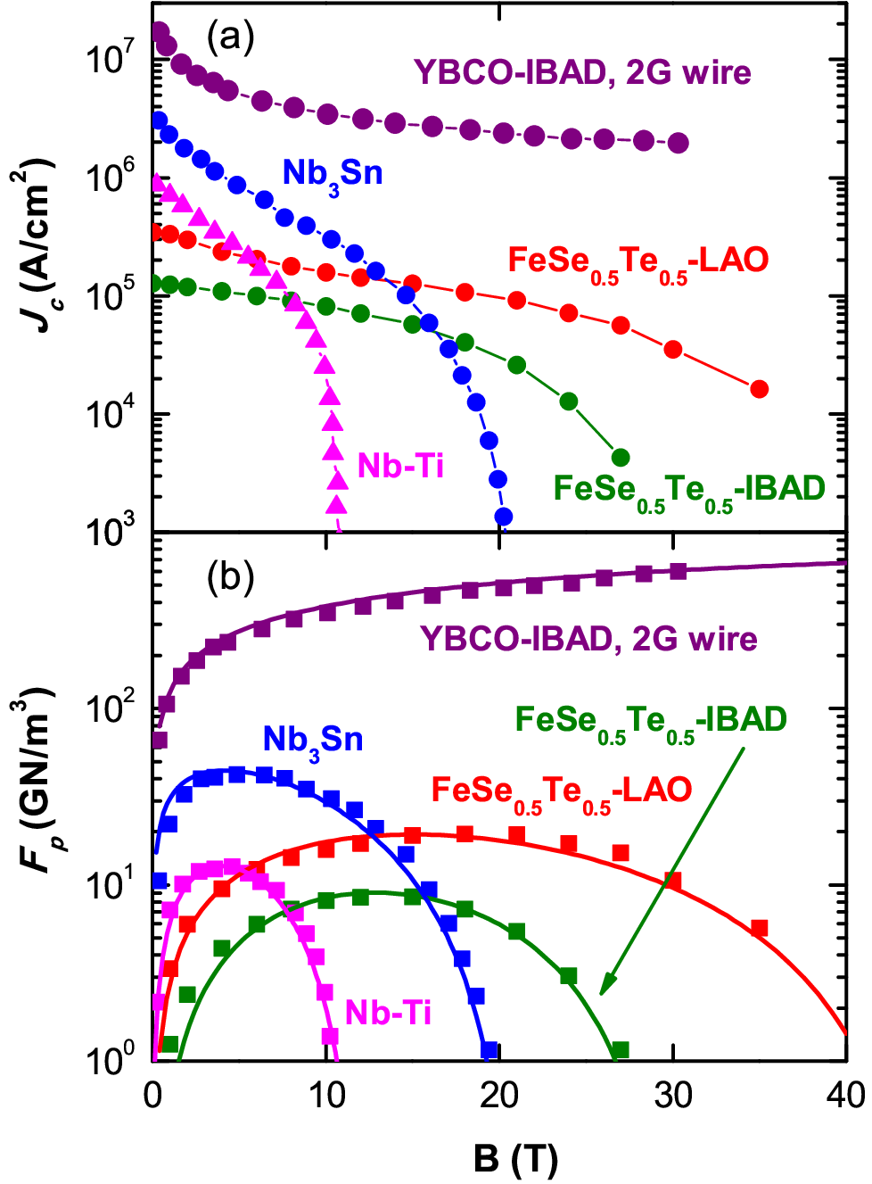
In Fig. 3 (b) we also show the Kramer’s scaling law approximation (solid line) for different types of superconductors at about 4.2 K, where is the normalized pinning force density and ( is defined as the onset of zero resistance) is the reduced field.[19] We found that for all types of superconductors, which is expected considering that the term describes the reduction of the superconducting order parameter at high field.[20] The low field term () was found for Nb3Sn and YBCO and is associated with the saturation regime, where changes little with the pinning center density because flux motion occurs by shearing of the vortex lattice, rather than by de-pinning.[21] The addition of BaZrO3 nano-rods, which are very effective pinning centers at 77 K, resulted in a very minor pinning increase at 4.2 K.[15] In contrast, the result of found in the FeSe0.5Te0.5 system is similar to the one in Nb-Ti.[20] This is a strong evidence of point defect core pinning, most likely from the inhomogeneous distribution of Se and Te. In the core pinning regime is a product of the individual times the pinning center density. This means that the of FeSe0.5Te0.5 can still be enhanced by simply adding more defects to act as pinning centers. Due to the short coherence length, we expect more pinning enhancement in FeSe0.5Te0.5 before reaching the coupling limit.
In conclusion, we have grown -axis oriented superconducting FeSe0.5Te0.5 coated conductors by pulsed-laser deposition. These tapes have a nearly isotropic above 104A/cm2 under 25 T of magnetic field at about 4.2 K. Pinning force analysis indicates a point defect pinning mechanism. These properties show that FeSe0.5Te0.5 has a very promising future for high field applications at liquid helium temperatures.
This work was supported by the U.S. Department of Energy, Office of Basic Energy Science, Materials Sciences and Engineering Division, under Contract No. DE-AC02-98CH10886. IBAD templates were provided by Los Alamos National Laboratory under funding from the U.S. Department of Energy, Office of Electricity. A portion of this work was performed at the National High Magnetic Field Laboratory, which is supported by National Science Foundation Cooperative Agreement No. DMR-0654118, the State of Florida, and the U.S. Department of Energy.
References
- [1] M. N. Wilson, Superconducting magnets (Clarendon Press, Oxford University Press, Oxford Oxfordshire, New York, 1983).
- [2] A. P. Malozemoff, S. Fleshler, M. Rupich, C. Thieme, X. Li, W. Zhang, A. Otto, J. Maguire, D. Folts, J. Yuan, H. P. Kraemer, W. Schmidt, M. Wohlfart, and H. W. Neumueller, Supercond. Sci. Technol. 21, 034005 (2008).
- [3] Z.-A. Ren, G.-C. Che, X.-L. Dong, J. Yang, W. Lu, W. Yi, X.-L. Shen, Z.-C. Li, L.-L. Sun, F. Zhou, and Z.-X. Zhao, Europhys. Lett., 83 17002 (2008).
- [4] F. Hunte, J. Jaroszynski, A. Gurevich, D. C. Larbalestier, R. Jin, A. S. Sefat, M. A. McGuire, B. C. Sales, D. K. Christen and D. Mandrus, Nature (London) 453, 903 (2008).
- [5] J. Jaroszynski, F. Hunte, L. Balicas, Y. J. Jo, I. Raicevic, A. Gurevich, D. C. Larbalestier, F. F. Balakirev, L. Fang, P. Cheng, Y. Jia, and H. H. Wen, Phys. Rev. B 78, 174523 (2008).
- [6] A. Yamamoto, J. Jaroszynski, C. Tarantini, L. Balicas, J. Jiang, A. Gurevich, D. C. Larbalestier, R. Jin, A. S. Sefat, M. A. McGuire, B. C. Sales, D. K. Christen, and D. Mandrus, Appl. Phys. Lett. 94, 062511 (2009).
- [7] S. Lee, J. Jiang, Y. Zhang, C.W. Bark, J. D.Weiss, C. Tarantini, C. T. Nelson, H.W. Jang, C. M. Folkman, S. H. Baek, A. Polyanskii, D. Abraimov, A. Yamamoto, J.W. Park, X. Q. Pan, E. E. Hellstrom, D. C. Larbalestier, and C. B. Eom, Nature Materials 9, 397 (2010).
- [8] P. Moll, R. Puzniak, F. Balakirev, K. Rogacki, J. Karpinski, N. D. Zhigadlo, and B. Batlogg, Nature Materials 9, 628 (2010).
- [9] M. G. Fang, J. H. Yang, F. F. Balakirev, Y. Kohama, J. Singleton, B. Qian, Z. Q. Mao, H. D. Wang, and H. Q. Yuan, Phys. Rev. B 81, 020509 (2010).
- [10] Daniel Braithwaite, Gerard Lapertot, William Knafo, and Ilya Sheikin, J. Phys. Soc. Japan 79, 053703 (2010).
- [11] W. Si, Z. W. Lin, Q. Jie, W. G. Yin, J. Zhou, G. Gu, P. D. Johnson, and Q. Li, Appl. Phys. Lett. 95, 052504 (2009); W. Si, Q. Jie, L. Wu, J. Zhou, G. Gu, P. D. Johnson, and Q. Li, Phys. Rev. B 81, 092506 (2010).
- [12] T. Ozaki, K. Deguchi, Y. Mizuguchi, Y. Kawasaki, T. Tanaka, T. Yamaguchi, S. Tsuda, H. Kumakura, and Y. Takano, arXiv:1103.0402.
- [13] D. Larbalestier, A. Gurevich, D. M. Feldmann, and A. Polyanskii, Nature (London) 414, 368 (2001).
- [14] C. Sheehan, Y. Jung, T. Holesinger, D. M. Feldmann, C. Edney, J. F. Ihlefeld, P. G. Clem, and V. Matias, Appl. Phys. Lett. 98, 071907 (2011); V. Matias, J. Hanisch, E. J. Rowley, and K. Guth, J. Mater. Res. 24, 125 (2009).
- [15] A. Xu, J. J. Jaroszynski, F. Kametani, Z. Chen, D. C. Larbalestier, Y. L. Viouchkov, Y. Chen, Y. Xie and V. Selvamanickam, Supercond. Sci. Technol. 23, 014003 (2010); Z. Chen, F Kametani, Y. Chen, Y. Xie, V. Selvamanickam and D. C. Larbalestier, Supercond. Sci. Technol. 22, 055013 (2009).
- [16] L. D. Cooley, P. J. Lee, and D. C. Larbalestier, Phys. Rev. B 53, 6638 (1996); D. C. Larbalestier and A. W. West, Acta Metall. 32, 1871 (1984).
- [17] A. Godeke, Supercond. Sci. Technol. 19, R68 (2006); R. M. Scanlan, W. A. Fietz, and E. F. Koch, J. Appl. Phys. 46, 2244 (1975).
- [18] S. Lee, J. Jiang, J. D. Weiss, C. M. Folkman, C. W. Bark, C. Tarantini, A. Xu, D. Abraimov, A. Polyanskii, C. T. Nelson, Y. Zhang, S. H. Baek, H. W. Jang, A. Yamamoto, F. Kametani, X. Q. Pan, E. E. Hellstrom, A. Gurevich, C. B. Eom, and D. C. Larbalestier, Appl. Phys. Lett. 95, 212505 (2009).
- [19] is used as a scaling field, , rather than , the characteristic field in the original Kramer’s scaling relation. has been found to give a better scaling behavior for in high- cuprates in general. In the case of iron chalcogenides, we found that scaling with either or gave similar exponents.
- [20] J. W. Ekin, Supercond. Sci. Technol. 23, 083001 (2010).
- [21] J. A. Good and E. J. Kramer, Philos. Mag. 24, 339 (1971).