General considerations of the electrostatic boundary conditions in oxide heterostructures
1 Introduction
When the size of materials is comparable to the characteristic length scale of their physical properties, novel functionalities can emerge. For semiconductors, this is exemplified by the “superlattice” concept of Esaki and Tsu, where the width of the repeated stacking of different semiconductors is comparable to the “size” of the electrons, resulting in novel confined states now routinely used in opto-electronics [1]. For metals, a good example is magnetic/non-magnetic multilayer films that are thinner than the spin-scattering length, from which giant magnetoresistance (GMR) emerged [2, 3], used in the read heads of hard disk drives. For transition metal oxides, a similar research program is currently underway, broadly motivated by the vast array of physical properties that they host. This long-standing notion has been recently invigorated by the development of atomic-scale growth and probe techniques, which enables the study of complex oxide heterostructures approaching the precision idealized in Fig. 1(a). Taking the subset of oxides derived from the perovskite crystal structure, the close lattice match across many transition metal oxides presents the opportunity, in principle, to develop a “universal” heteroepitaxial materials system.

Hand-in-hand with the continual improvements in materials control, an increasingly relevant challenge is to understand the consequences of the electrostatic boundary conditions which arise in these structures. The essence of this issue can be seen in Fig. 1(b), where the charge sequence of the sublayer ‘‘stacks’’ for various representative perovskites is shown in the ionic limit, in the (001) direction. To truly ‘‘universally’’ incorporate different properties using different materials components, be it magnetism, ferroelectricity, superconductivity, etc., it is necessary to access and join different charge sequences, labelled here in analogy to the designations ‘‘group IV, III-V, II-VI’’ for semiconductors. As we will review, interfaces between different families creates a host of electrostatic issues. They can be somewhat avoided if, as in many semiconductor heterostructures, only one family is used, with small perturbations (such as n-type or p-type doping) around them11 1 These effects can in principle also be reduced by choosing a (110) growth orientation, but other aspects of stability may be limiting [5].. However, for most transition metal oxides, this is greatly restrictive. For example, LaMnO3 and SrMnO3 are both insulators in part due to strong electron correlations, and only in their solid solution does “colossal magnetoresistance” emerge in bulk [6]. Similarly, the metallic superlattice shown in Fig. 1(c) can be considered a nanoscale deconstruction of (La,Sr)TiO3 to the insulating parent compounds. Therefore the aspiration to arbitrarily mix and match perovskite components requires a basic understanding of, and ultimately control over, these issues.
In this context, here we present basic electrostatic features that arise in oxide heterostructures which vary the ionic charge stacking sequence. In close relation to the analysis of the stability of polar surfaces and semiconductor heterointerfaces, the variation of the dipole moment across a heterointerface plays a key role in determining its stability. Different self-consistent assignments of the unit cell are presented, allowing the polar discontinuity picture to be recast in terms of an equivalent local charge neutrality picture. The latter is helpful in providing a common framework with which to discuss electronic reconstructions, local-bonding considerations, crystalline defects, and lattice polarization on an equal footing, all of which are the subject of extensive current investigation.
2 The polar discontinuity picture
2.1 Stability of ionic crystal surfaces
The surface of crystals determines many of their physical, mechanical and chemical properties. Due to the lack of translational symmetry in the perpendicular direction, the stable charge distribution at the surface can be completely different from that of the bulk, and the surface may reconstruct in a manner different from the bulk states. Imagine an ideal ionic crystal which consists of charged ions bound together by their attractive interactions, and all the ions are taken as fixed point charges. Since the charges are locally preassigned to the ions in this model, the ideal ionic surface apparently requires no reassignment of the charges from that of the bulk. However, the electrostatic potential in an ionic crystal diverges when there is a dipole moment in the unit cell perpendicular to the surface. The potential22 2 Note that literature on this topic uses both the electrostatic potential (for a positive test charge) and the electron potential energy (as in band diagrams) — we use the former here. should be constant in vacuum in the absence of external fields, and the potential can be obtained by integrating the electric field caused by the charged sheets, as shown in Fig. 2. A finite shift in the potential emerges due to the dipole moment of each unit cell, and as the unit cells are stacked, so the potential grows, and diverges into the crystal. Due to this effectively infinite surface energy, such surfaces cannot exist without reconstructions, and the stability of an ionic surface randomly cut from the bulk is not trivial without knowing the stacking sequence of the charged sheets precisely. This surface instability and the associated reconstructions have been indeed observed by means of low-energy electron diffraction (LEED) and ion scattering, where absorption of foreign atoms, surface roughening, or changes in surface stoichiometry were found [7, 8, 9].

In order to survey the stability of such surfaces, Tasker introduced a classification of the surfaces from the viewpoint of the charge of the atomic sheets and the dipole in a unit cell which starts from the top-most layer [10]. Note he discussed the stability of bulk frozen surfaces33 3 This definition of “bulk frozen” follows description of Goniakowski et al. [11]., where the top-most layer is one of the constituent atomic sheets of the bulk crystal and has no reconstruction. Tasker described three types of the surfaces, as shown in Fig. 3:
- •
Type 1 has equal numbers of anions and cations on each plane, and therefore the unit cell has no dipole moment. For example, the (001) and (110) surfaces of the rocksalt structure (e.g. NaCl, MgO, NiO) are classified as this type.
- •
Type 2 has charged planes, but no net dipole moment perpendicular to the surface. The anion terminated (001) surface of the fluorite structure (e.g. UO2, ThO2) is an example.
- •
Type 3 has charged planes and a net dipole moment normal to the surface. Examples include the (111) surface of the rocksalt structure, and (001) or (111) surfaces of the zincblende structure (e.g. GaAs, ZnS).
In Tasker’s classification, type 1 and type 2 surfaces are stable while type 3 is not, since the instability of the surface comes from the stacking of the dipole in each unit cell. Macroscopically, the instability of the type 3 surface arises from the change in the potential slope when crossing the surface. The term “polar surface” can be defined following this classification, namely we call a surface “non-polar” when it is type 1 or type 2, and “polar” when it is type 3.

These definitions are analogous to the definition of polar crystals, although polar surfaces and surfaces of polar crystals are not equivalent. Dielectric polarization is observed when an electric field is applied to a material, but even in the absence of the field, some crystals retain a “spontaneous” polarization [12]. Only 10 out of 32 point groups show this behavior, and their members are called polar crystals, while the others are non-polar. Twenty-one out of 32 point groups do not have inversion centers, and the polar crystals are included among them. When a material shows macroscopic spontaneous polarization, the electrostatic potential of one end is different from the other end as a result of the stacking of the dipole in each unit cell, and the surface usually has “compensating” charge to reconcile this potential difference. Since Tasker took unit cells from the top-most layer, even crystals with inversion symmetry can show dipoles in the unit cells in his model. For example, although NaCl is cubic and has inversion symmetry, its (111) surface is classified into type 3. Therefore, the word “polar” should be used with some care since it has different meanings in different contexts.
2.2 Stability of covalent surfaces
At the surface of covalent crystals, lacking full coordination, the top-most atoms have valence electrons which are not used for bond formation. These non-bonding electrons are called dangling bonds, and have higher energy than the bonding electrons, which causes the movement of the atom positions to decrease their number [13].
In a covalent crystal, since the bonds are formed as a hybridization of the valence electrons of charge-neutral atoms, one can describe the charge distribution starting from a bulk unit cell which is charge neutral and dipole-free. However, when the electronegativity of the atoms are different e.g., Ga and As in GaAs, charge transfer between anions and cations occurs, similar to the ionic case. This charge transfer is realized by the difference of the contribution of each bond, namely electrons to the anions and electrons to the cations. Here is a parameter to describe the ionicity of the bond, determined by the electronegativity of the two bonding atoms. As a consequence, the unit cell can have a dipole moment normal to the surface, which causes the same instability as that in the ionic crystal case. Therefore, even in a covalent crystal, a surface instability emerges from the dipole in the unit cell, independent of the surface instability naturally arising from dangling bond formation. Even though Tasker’s classification was introduced to describe the stability of ionic surfaces, it is also relevant for covalent surfaces in the presence of finite ionicity.
Both dangling bond formation and the instability of polar surfaces are at play, and they are reconciled simultaneously at the surface of covalent crystals. Therefore, direct observation of the instability of polar surfaces in covalent systems has been difficult. When we consider an epitaxial interface which has similar charge structure as the polar surface, the instability from the dangling bonds disappears, and we can solely discuss the stability in the same manner as that for the ideal ionic surfaces, as discussed in the next section.
2.3 Polar semiconductor interfaces
Similar to the instability of polar surfaces, dipoles in the unit cells stacking from the interface can cause potential divergence and instability, and require reconstruction. This point was first proposed at the heteroepitaxial interface of GaAs and Ge in the [001] direction by three groups from different starting points for treating ionicity. Based on their considerations, we define polar and non-polar interfaces, in analogy to polar and non-polar surfaces.
2.3.1 Charge transfer based on electronegativity
Frensley and Kroemer calculated the energy band diagram at abrupt semiconductor heterojunctions [14]. Their starting point was to describe the alignment of atoms around the interface without considering the ionicity, and then calculate the charge transfer based on the ionicity using the electronegativity of the atoms, under assumption that the charge transfer only occurs between the nearest neighbors. The Phillips electronegativity values were used (, , and [15]). In the bulk zincblende structure AB, the A site is tetrahedrally coordinated by four B atoms and vice versa, and based on their calculation [16], the ionic charges of the atoms are given by
| (1) |
where is the elementary charge. This is equivalent to assuming a charge transfer of between any pair of the nearest neighbors.
Consider the case of Ge/GaAs interfaces as shown in Fig. 4(a), where the charge on the Ga ions adjacent to the interface is
| (2) |
Similarly, the charges on the Ge ions at the interface and at the As sites are and .

Without ionicity, the electrostatic potential is constant, and even with ionicity, the potential does not diverge. This can be understood easily by tracking the virtual charge transfer processes from the starting alignment of the charge neutral atoms. The charge transfer is equivalent to the situation that each neutral atom loses charges, and half of them are transferred to the left atoms and the other half to the other side, as shown in Fig. 4(b). Therefore, charges are always transferred symmetrically, and each modulation creates no dipole, resulting in no potential shift. Here, a change of the number of electrons in the ions compared to the bulk state is assumed, which is equivalent to changing the valence assignments.
2.3.2 Self-consistent calculation and counting electrons of bonds
Baraff et al. performed a self-consistent calculation of the potential, charge density, and interface states for the abrupt interface between Ge and GaAs, terminated on a (001) Ga plane [17]. As shown in Fig. 5(a), their calculation showed fractional occupancy of electronic states only at the interface, which cannot exist in bulk.

These interface states can be discussed from a local-bond counting point of view as well. The number of the valence electrons is 4 for Ge, 3 for Ga, and 5 for As. When we assume all the valence electrons of an atom are equally distributed to the four covalent bonds around it, Ge, Ga, and As atoms supply 1, 0.75, and 1.25 electrons to each bond, respectively. As shown in Fig. 5(b), the Ge-Ga bonds at the interface have 1.75 electrons per bond, while other bonds have 2 electrons in each. These partially occupied bonds are considered to form the interface states.
When the number of electrons are smaller than that in the bulk, the attractive interaction between the bonded atoms should be weaker. According to their calculation, the energy is minimized when the Ge-Ga bond length is 4 % larger than that of the bulk. Without the change of the bonding length, the system requires long-range disturbance of the lattice, which is unlikely to be realized.
2.3.3 Solving the potential divergence from the ionic picture
Both the charge transfer model by Frensley and Kroemer and the electron counting model by Baraff et al. predict (indeed require) that there are interface states at a Ge/GaAs (001) interface even if it is perfectly abrupt, with no crystalline defects. The central point raised by these studies is that despite having the same crystal structure, and having very closely matching lattice constants, this interface must accomodate charge arising from interface boundary conditions. However, experimentally no considerable density of interface states was observed [18], and a model to treat this interface without changing the number of charges at the interface was required.
Harrison et al. constructed a model for the Ge/GaAs (001) heterojunctions by stacking the fully ionized atoms, and calculated the electrostatic potential based on the fixed assignment of the charges [19]. As shown in Fig. 6(a), the potential is very similar to the case of polar surfaces since the unit cells which start from the interface have dipoles in GaAs, while the unit cells in Ge are always charge neutral. Therefore, the stacking of the dipoles causes potential divergence in this case as well.

Since the charge of each ion was fixed, the solution to the instability of this interface requires compensation by changing the stoichiometry at the interface. They proposed a simple model where 1/4 of the Ge atoms are replaced by As atoms at the interface while 1/4 of the Ga atoms adjacent to the interface are replaced by Ge. In this reconstructed model with two transition layers, the electrostatic potential does not diverge, as shown in Fig. 6(b).
It might be surprising that from two completely different starting points, namely one from covalent (Frensley and Kroemer) and the other from ionic (Harrison et al.) pictures, exactly the same potential diagrams were obtained. However, rearranging the number of charges at the perfectly abrupt interface or changing the interface composition while maintaining the ionic charges of the atoms can give the same net charge distribution. The experimental absence of localized states suggests the atomic reconstruction based on the ionic picture. This is equivalent of saying that the electronic state at this semiconductor heterointerface cannot deviate so strongly from that of the bulk constituents — it is energetically inaccessible. This is the fundamental aspect which can be quite different in complex oxide heterointerfaces, and is the subject of much current excitement. Namely, there is a possibility that the charge transfer picture (Frensley and Kroemer) and the electron counting picture (Baraff et al.), which require large deviations of electron numbers from the bulk values, can be energetically accessed in transition metal oxides with multi-valency, as described in Section 3.
2.3.4 Definition of the polar interface
Following the model by Harrison et al., we can define the polar nature of a bulk frozen interface between two materials, where the interface consists of two bulk frozen surfaces connected together44 4 Here, we consider only interfaces between two semi-infinite materials — we ignore the coupling to other interfaces or surfaces, which is discussed in Sections 4.3 and 4.4.. First let us classify the interfaces by the polar nature of the two constituent surfaces, as shown in Fig. 7.

- •
Type I is formed between two non-polar surfaces, and the potential is flat.
- •
Type II is formed between polar and non-polar surfaces, and the potential diverges from the interface in the material with the polar surface.
- •
Type III is formed between two polar surfaces, and the direction and the size of the dipoles in the unit cells which start from the interface is the same. Although looks to diverge from the interface in both materials, there is no macroscopic difference in the potential slope across the interface. We can cancel the potential slope on both sides by adding a constant electric field, as shown in Fig. 7(c). Therefore, this interface is stable as constructed.
- •
Type IV is formed between two polar surfaces, where the dipoles in the two different unit cells are not identical, which results in a macroscopic difference in the potential slope at the interface. It is impossible to find any constant electric field to cancel out the potential divergence in both media, due to this difference55 5 Note type IV is the most common and general case in reality, since the electronegativity can never perfectly match between different materials..
Type I and type III are stable due to the absence of a macroscopic difference of the potential slopes, while type II and type IV are not stable. This difference arises from the continuity/discontinuity of the dipoles in the unit cells which start from the interface. A bulk frozen interface is non-polar, when the dipoles in the unit cells starting from the interface are identical across the interface, and thus no change of the macroscopic potential slope exists. On the other hand, it is polar if a bulk frozen interface has a discontinuity of the dipole moment in each unit cell. For example, from a purely ionic viewpoint (Harrison et al.) the abrupt Ge/GaAs (001) interface is classified as type II, and thus polar.
This definition of the polar nature of interfaces is consistent with that of surfaces. When the vacuum is treated as a charge neutral medium, the non-polar surface is type I, and the polar surface is type II in this classification of the interfaces, and the polar nature is maintained following the definitions for the interface. We can treat surfaces and interfaces in one framework, which is the polar nature of discontinuities at materials boundaries. In summary, polar discontinuities, which consist of polar surfaces and interfaces, are unstable due to the macroscopic potential folding arising from the discontinuity of the stacking of dipoles in the unit cells, and require reconstructions to stabilize them. Interfaces with continuous polarity, on the other hand, are stable without any reconstructions.
3 Metallic conductivity between two insulators
As noted in the introduction, the modern ability to approach atomic control in complex oxide heterostructures has newly enabled the experimental investigation of their polar discontinuities. As illustrated in Fig. 1(a), an immediate question arises regarding the choice of the termination layer at the interface, and the consequences of this degree of freedom. This issue has been most explicitly raised, and hotly debated, for the electron gas observed at the interface of two perovskite insulators, LaAlO3 and SrTiO3 [20]. Specifically, the (001) heterointerface was found to be insulating when grown using a SrTiO3 substrate which was SrO-terminated, and conducting when TiO2-terminated. Given the rapid evolution of the field, and the numerous reviews of this heterostructure in the literature, we do not attempt a comprehensive review here. Instead the LaAlO3/SrTiO3 interface will be used to illustrate the various mechanisms suggested to explain the interface electronic structure, and the electrostatic boundary conditions which arise. It should be stressed, however, that all oxide heterointerfaces should be considered type IV to varying degrees, and thus these issues are quite general – even underlying the interface charge in the superlattice shown in Fig. 1(c).
3.1 The polar discontinuity scenario
Assuming pure ionicity, the charge sequence of the (001) perovskite planes are different in these two materials, namely the planes of LaAlO3 are (La3+O2-)+ and (Al3+O)-, while those of SrTiO3 are (Sr2+O2-)0 and (Ti4+O)0. Therefore, the abrupt interface between LaAlO3 and SrTiO3 is type II polar66 6 Allowing for covalency, SrO and TiO2 planes in SrTiO3 are no longer charge neutral, and thus the (001) surface is weakly polar, but still the dipole size of the unit cells which start from the interface is different from that of LaAlO3. and requires reconstruction as shown in Fig. 8, just as for the GaAs/Ge (001) interface.
Unlike polar semiconductor interfaces where only atomic reconstructions are available due to the fixed ionic charge of each element77 7 While here we discuss large scale charge modifications, small polar discontinuities can induce free carriers in semiconductors, such as in AlGaN/GaN heterostructures [21, 22]., we have another possibility to reconcile the instability of polar interfaces, through electronic reconstructions [23]. At the LaAlO3/SrTiO3 interface, when the interface termination is LaO/TiO2, it requires a net half negative charge per 2D unit cell to reconcile the potential divergence (n-type). Accessing Ti3+ can source this negative charge by accommodating electrons at the Ti 3 level, as was spectroscopically observed [24]. On the other hand, when the interface is terminated by AlO2/SrO, the sign of the required charges is opposite (p-type). Due to the difficulty of accommodating holes in this structure (such as Ti5+), the positive charges are realized by the formation of oxygen vacancies close to the interface, as inferred from measurements of the O-K edge fine structure. Oxygen vacancies are known as electron donors, but in this case they are formed to provide positive charges, and thus no electrons are supplied from these vacancies compensating the polar discontinuity. Therefore the system does not have itinerant electrons and remains insulating [20, 25].

One of the key corollaries of this scenario is the LaAlO3 thickness dependence. This is because the size of the potential difference arising from the stacking of the dipoles in the unreconstructed structure is finite in thin films, and if it is small enough, the system may be stable without any reconstruction. Indeed, a critical thickness of LaAlO3 was observed [26], where the n-type LaAlO3/SrTiO3 interface is insulating if the thickness of LaAlO3 is up to 3 unit cells, and metallic above that thickness. A similar tendency was also observed in SrTiO3/LaAlO3/SrTiO3 trilayer structures where the distance between the two polar interfaces was varied [27].
3.2 Oxygen vacancy formation during growth
SrTiO3 is known to be a material which readily accommodates oxygen vacancies that act as donors to provide itinerant electrons [28, 29]. Either kinetic bombardment of the SrTiO3 substrate by the ablated species (early studies of this interface all used pulsed laser deposition), or gettering by a reduced film, can induce oxygen vacancies, and they were suggested to be the dominant origin for the observed conductivity by several groups [30, 31, 32]. Indeed, the first report found a strong dependence of the Hall density for n-type interfaces on the oxygen partial pressure () during growth, while the p-type interface was robustly insulating [20]. For n-type samples with similar variations in the transport properties, Kalabukhov et al. found when grown at Torr, the samples exhibited blue cathode- and photo-luminescence at room temperature [30], similar to that of reduced SrTiO3 by Ar bombardment [33]. In addition to transport studies, Siemons et al. demonstrated that the photoemission spectra from these interfaces showed a larger amount of Ti3+ in samples grown at low pressures without oxygen annealing [31]. Herranz et al. observed Shubnikov-de Haas oscillations in reduced LaAlO3/SrTiO3 samples which were quite similar to bulk doped SrTiO3, and rotation studies indicated a three-dimensional Fermi surface [32].
The strong dependence of the conducting channels in LaAlO3/SrTiO3 was observed and mapped by means of conducting tip atomic force microscopy on cross-sections of the interface, which revealed a conducting region extending into the substrate for samples grown at low pressure [34], as shown in Fig. 9. After annealing, the width of the conductive layer decreased to , as limited by the radius of the probing tip. The consensus of these and other studies was that the free carriers in samples grown at low were dominated by oxygen vacancies, since the density far exceeded that needed to stabilize the polar discontinuity. For high , or after post-annealing, the origin was less clear.

3.3 Intermixing and local bonding at the interface
Willmott et al. studied a five unit cell film of LaAlO3 on SrTiO3 (001) by means of surface x-ray scattering [35], using coherent Bragg rod analysis (COBRA) [36] and further structural refinement. Their analysis revealed intermixing of the cations (La, Sr, Al, and Ti) at the interface [Fig. 10(a)], as well as significant local displacement of the atomic position both in the film, and in SrTiO3 close to the interface [Fig. 10(b)]. The distribution of Ti valence was also inferred by minimizing the electrostatic potential [Fig. 10(c)] following the obtained atomic positions, and the atomic displacements were explained by the larger ionic radii of Ti3+ compared to Ti4+ [Fig. 10(d)]. Based on these observations, the origin of the interface conductivity was suggested to be the formation of the bulk-like solid solution La1-xSrxTiO3 in a region of approximately 3 unit cells. This explanation can be considered a diffused version of local bonding arguments — i.e., that even in the abrupt limit, the Ti at the interface has La on one side, and Sr on the other.

3.4 Reconciling the various mechanisms
At present, it can be fairly stated (we believe) that no one scenario can completely explain the vast and growing body of experimental work on this system. Even theoretical calculations show an extreme sensitivity to the choice of boundary conditions and assumptions of site-occupancy [37, 38, 39, 40, 41]. To give examples for each perspective: The polar discontinuity picture should lead to a significant internal field in ultrathin LaAlO3, while experiments [42] put an upper bound far below that expected theoretically, even allowing for significant lattice polarization [43]. Oxygen vacancies induced by growth are difficult to reconcile with the notion that a single layer of SrO can prevent their formation. Local bonding and interdiffusion considerations do not address the constraints of global charge neutrality. Furthermore, discriminating between these mechanisms is often difficult, since the change of Ti valence shows similar transport, spectroscopic, and optical properties, independent of its origin.
It is extremely likely that multiple contributions exist to varying degrees, dependent on the growth details of a given sample. While this is a matter for further experimental investigation and refinement, an equally difficult issue appears to be one of semantics. For example, one of the conceptual difficulties of the polar discontinuity picture has been the question: Where do the electrons come from? In many presentations [24, 26, 44, 45], the charges at the interface are depicted to originate from the surface of the LaAlO3 film, but it is not so obvious that they travel through the insulating films independent of its thickness [26]. Fundamentally, the “non-locality” of these electrostatic descriptions has sometimes been considered less intuitive and compelling than “local chemistry” mechanisms such as vacancies or interdiffusion [30, 31, 34, 46, 35].
A related difficulty is how to treat the charge density to describe the macroscopic electric field. Based on the polar discontinuity picture, the stacking of the dipoles in the unit cells creates a macroscopic electric field, resulting in the change of the potential slope at the discontinuity. In this picture, the unit cells start from the discontinuity, and thus the composition is always the same as that of the bulk, which is charge neutral. It might be strange that the potential starts to bend at the discontinuity although all the unit cells start out charge neutral, because the source of an electric field is charge. In fact, the source is the macroscopic bound charge density at the interface, as discussed in Section 5, but the existence of such implicit charge density has caused a fair bit of confusion. To address these concerns, it is useful to treat the electrostatics in a purely local description, as well as the boundary charges explicitly. Furthermore, the effects of defects and diffusion can be discussed more simply by re-framing the polar discontinuity picture in local form. Therefore, this local charge neutrality picture based on dipole-free unit cells is developed in the next section first for idealized models, followed by discussion of incorporation of chemical defects.
4 The local charge neutrality picture
4.1 Unit cells in ionic crystals
One of the origins of confusion regarding the stability and reconstructions of polar discontinuities arises because of the various choices of a unit cell in a crystal, which determines the size and direction of the dipole in it88 8 For simplicity, we started our discussion from a point-charge model of ions, and neglect the free carrier distribution. More generally, the charge distribution can be described using contributions from ion cores and free carrier Wannier functions, and the ambiguity of the choice of unit cells appears in this extended case as well [47]. . For example, when we take the unit cell of LaAlO3, this stacking can be treated as a dipole of [(AlO2)- (LaO)+], as shown in Fig. 11(a). However, it is also possible to take [(LaO)+ (AlO2)-] as a unit cell, and the sign of the dipole is opposite to the previous case, as shown in Fig.11(b).
The choice of unit cells should not change the electrostatic potential in the crystal. Indeed, the difference between the two choices is compensated by the potential arising from the surface layer. If the surface is terminated by the (AlO2)- layer, it remains as an extra negatively charged layer when we take [(LaO)+ (AlO2)-] as the unit cell, as shown in Fig.11(b), and the total electrostatic potential remains the same as in the [(AlO2)- (LaO)+] unit cell case.

Therefore, it is impossible to fix the direction of the dipoles without knowing the surface termination. In other words, it is the surface that determines the stability of the system. So the problem can be simplified by considering the surface locally, and not by counting the number of dipoles in the material. In order to avoid the dipoles arising from the stacking of charged layers, the simplest approach is to take dipole-free unit cells. This can be achieved in any crystal [11], and in the LaAlO3 case, this is done by taking [(LaO) - (AlO2) - (LaO)] (or [(AlO2) - (LaO) - (AlO2)]) as a unit cell, as shown in Fig. 11(c). This is analogous to the unit cell in a type 2 model in Tasker’s classification. From group theory, it is known that spontaneous polarization can be observed only in a direction where the crystal does not have mirror symmetry. Since cubic perovskites do have mirror symmetry in the [001] direction (we neglect surface or interface induced lattice polarization for now), it is useful to take dipole-free unit cells to reflect the lack of polarization in the bulk.
When we take this unit cell, the stability of a polar surface or interface can be discussed by only considering the charge neutrality of each unit cell, since now there is no net dipole created by the stacking of charged layers. For example, the instability of the (AlO2) terminated surface of LaAlO3 is naturally derived because the top-most unit cell is [(AlO2)- (LaO)+]-0.5, which violates charge neutrality, as shown in Fig. 11(c). Thus the (001) surface of LaAlO3 cannot keep the bulk termination, either by an AlO2 or LaO layer, and must reconstruct to compensate this charge [48, 49]. Once charge neutrality of all the unit cells is achieved, the system is free to undergo electron / hole modulation or interdiffusion / displacement of the atoms, which creates only finite dipoles and does not violate neutrality99 9 The effect of diffusion is further discussed in Section 6.1 as an example of sources of such finite dipoles. Another source of interface dipoles, the quadrupolar discontinuity, is discussed in Section 6.3.. These perturbations are important because they determine the real charge structure, for example via lattice distortion close to the surface of LaAlO3 [48, 49].
Following these arguments, the polar nature of given bulk frozen surfaces and interfaces is clearly defined, considering local charge neutrality using dipole-free unit cells: a bulk frozen surface or interface is polar if the unit cell at the surface or interface cannot keep charge neutrality when we take dipole-free unit cells in the bulk.
4.2 LaAlO3/SrTiO3 in the local charge neutrality picture

Taking dipole-free unit cells of perovskites O3 in the [001] direction, namely [(O) - (O2) - (O)], the interface unit cell can be treated as a -dopant at the interface. As shown in Fig. 12, the interface unit cell does not keep the stoichiometry of either of the bulk materials, not even a simple mixture of them. This issue is actually one of the central opportunities of the interface science of heterostructures. Namely, the LaO/TiO2 terminated LaAlO3/SrTiO3 interface has La0.5Sr0.5TiO3 as the interface unit cell. Considering the formal electronic charges of La3+, Sr2+, and O2-, the Ti ion in this unit cell should take Ti3.5+ as a formal valence, which is the same reconstructed state as that for the previous discussion by the polar discontinuity picture.
Similarly, the AlO2/SrO terminated interface has La0.5Sr0.5AlO3 as the interface unit cell, and due to the fixed ionic charges of the elements, such a unit cell is not charge neutral and thus unstable: (LaSrAl3+O)0.5-. Instead, allowing a change of the oxygen number in the interface unit cell, La0.5Sr0.5AlO2.75 is charge neutral1010 10 This composition is not stable in bulk perovskite form, but can be considered as a mixture of the bulk compounds, LaAlO3, Sr3Al2O6, and SrAl2O4, stabilized epitaxially at the interface., and the decrease of the oxygen content at the interface to stabilize a p-type LaAlO3/SrTiO3 interface is naturally derived. Note in this case, these oxygen vacancies are introduced to keep charge neutrality, and thus do not provide any free electrons. Thus, the electrons/oxygen vacancies to reconcile the polar instability of the bulk frozen LaAlO3/SrTiO3 interfaces are supplied by the interface unit cell itself.
In semiconductors, -doping is usually achieved in a symmetric geometry [50], that is the dopant layer is sandwiched between the same host material. In the LaAlO3/SrTiO3 case, by contrast, the two sandwiching materials have different band structure, with SrTiO3 having the narrower bandgap. Therefore, broadening of the charge distribution from the -dopant occurs only in the SrTiO3 side [46]. Figure 13 shows how the LaAlO3/SrTiO3 interface can be depicted in a semiconductor energy band diagram.

4.3 Coupling of polar discontinuities
When two polar discontinuities are brought in proximity to one another, coupling of the charges can occur to minimize the total energy of the system. This is just like the coupling of dopant layers in -doped semiconductor heterostructures, which can be understood in terms of depleted and undepleted structures. Figure 14(a) shows the band diagram of an undepleted semiconductor with one layer of -dopant. Since the dopant is positively ionized, an equal number of free electrons are left, and they screen out the potential created by the -dopant. As a consequence, the structure is neutral, and has zero electric field sufficiently far away from the -dopant layer.
On the other hand, Fig. 14(b) shows the band diagram of a depleted -doped structure, where the number of donors is equal to that of acceptors, and they are sufficiently close in space. As a result, all the free carriers recombine and the structure is depleted. The critical parameters to treat electronic coupling of two -doping layers are the distance between them and the dielectric constant of the medium. When the distance between them is smaller than the length scale of band bending of the undepleted structure, they couple and the system goes to a depleted state. Note in this case, charge neutrality in the neighborhood of one dopant layer is not necessarily maintained. Superlattice calculations using density functional theory show that the above threshold is observed by changing the thickness of each layer in LaAlO3/SrTiO3 superlattices, which can be captured in terms of a simple capacitor model [40, 41].

In -doped semiconductor heterostructures, only considering modulation of free carriers is sufficient to describe the coupling of the -dopant layers. However, when the system allows possibilities of excess charges other than the free carriers, which come from outside of the constructed crystal – e.g., anion or cation vacancies or foreign atoms absorbed to the surface, the electrostatic potential can be minimized via them. For example, the instability of the polar AlO2-terminated LaAlO3 surface can be solved by introducing positively charged surface oxygen vacancies [49]. The LaAlO3 thickness dependence of LaO-TiO2 terminated LaAlO3/SrTiO3 can be explained by a simple assumption, where we only consider coupling of the free electrons provided by the LaAlO3/SrTiO3 interface and the surface oxygen vacancies to keep the local charge neutrality of the polar LaAlO3 surface. Figure 15 shows a schematic structure of the LaAlO3/SrTiO3 heterojunction, where two polar discontinuities exist at the LaAlO3/SrTiO3 interface and the LaAlO3 surface. When the LaAlO3 film is sufficiently thick [Fig. 15(a)] these polar discontinuities are decoupled and charge neutrality is preserved locally by introducing oxygen vacancies at the surface and taking the Ti valence of at the interface unit cell. Fractionally filled Ti valence provides itinerant electrons, and therefore the system is metallic in the thick limit.
If the two polar discontinuities are brought closer [Fig. 15(b)], the external charges and the free carriers (surface oxygen vacancies and extra electrons in Ti valence) can recombine in an environment with oxygen gas, and the system is depleted and the conductivity disappears1111 11 This is similar to the recombination of free electrons and holes, and the actual recombination can be written by following Kröger-Vink notation [51] as: .. Here, the word “deplete” is used to mean “reduce the amount of charge other than charge bound to the crystal”, and the full depletion of the LaAlO3 surface means extinguishing the positively charged oxygen deficiency at the surface — i.e. the surface turns to an unreconstructed bulk frozen state. Manipulating this transition appears to roughly capture the essence of writing nanoscale features [44], which corresponds to the “writing” of surface charge [52].

4.4 Modulation doping by a proximate polar discontinuity
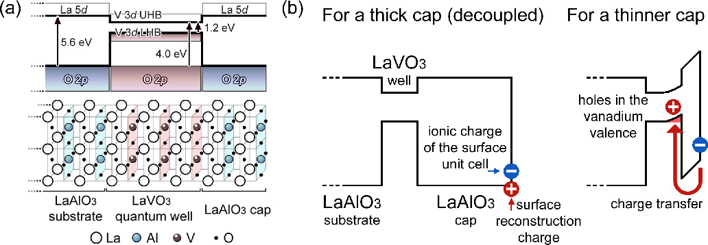
Even in systems containing only one polar discontinuity, coupling between the polar discontinuity and the other layers can occur in analogy to modulation doping by a -doping layer [53], as shown in Fig. 16. At the semiconductor interface, lineup of the conduction and valence bands should be maintained, as well as a fixed chemical potential, which causes the modulation of carriers resulting in band bending.
Assume an interface between two intrinsic semiconductors A (narrow bandgap) and B (wide bandgap). If the -dopant in B is sufficiently far from A, the flat band condition at the interface is maintained [Fig. 16(a)]. When A is brought in proximity to the -dopant in B, in order to keep the conduction band lineup, the conduction band minimum of A lies at lower energy than the chemical potential in B [Fig. 16(b)]. Since the free carriers around the -dopant in B have higher energy than the conduction band minimum of A, they transfer to A and band bending occurs in A [Fig. 16(c)]. As a result, the -dopant in B is depleted, and A is doped close to the interface.

An experimental example of such charge modulation was observed from a type 3 polar surface of LaAlO3 (001), which acts as a -dopant, to a narrow layer of the Mott insulator LaVO3 with smaller bandgap, as shown in Fig. 17 [54, 45]. This system is noteworthy in the discussion of polar discontinuity effects, in that the observed hole-doping can neither arise from oxygen vacancies nor interdiffusion.
4.5 Advantages of the local charge neutrality picture
As discussed, the local charge neutrality picture gives a clear and self-consistent explanation for the various phenomena at surfaces and interfaces. The stability of given surfaces and interfaces can be simply judged by looking at the local composition. When the interface composition differs from that of the bulk or a simple superposition of them, a different electronic and/or atomic state can be expected. Enforcing local charge neutrality at the interface unit cell naturally explains the source of the charges which can change the stoichiometry or the electron number of the constituent atoms from those of the bulk. For example, in a LaO/TiO2 terminated LaAlO3/SrTiO3 bulk frozen interface, the interface unit cell is La0.5Sr0.5TiO3 and the Ti is to achieve charge neutrality. Therefore, the difference between the Ti4+ in the bulk SrTiO3 and the interface Ti3.5+ comes from the interface unit cell itself, and not from anywhere else.
Another advantage of taking the local charge neutrality picture becomes clear when we discuss the coupling of polar discontinuities. The stability of the system can be discussed through the distance between the polar discontinuities and the screening length of the host material. In other words, the stability is determined by the balance of the activation energy of the dopant and the electrostatic energy allowing polarization of the media between the dopant layers. Therefore, the total polarizability of the media can be considered in the calculation, and is connected to the bulk permittivity in the thick limit. Note when the media is thin, the local effective permittivity is non-trivial since the local atomic displacements can be different from that in the bulk, and the local dielectric approximation breaks down [55].
5 Equivalence of the two pictures
Thus far we have discussed boundary conditions based on two different choices for the unit cell. This was implicitly taking a microscopic viewpoint, since the electric field and the total charge density were connected by Gauss’ law: , where is the vacuum permittitivity. Since is used (hence the atomic-scale stepped or sawtooth potentials), different choices for the unit cell were irrelevant so long as global charge neutrality was considered. Here we confirm the equivalence of the two pictures from the macroscopic electrostatic viewpoint.
5.1 Gauss’ law for infinite crystals
In media, treating is often quite complicated, which can be simplified by using the electric displacement :
| (3) |
where is the polarization. Then Gauss’ law is given by
| (4) |
where is the free charge – the part of the macroscopic charge density due to excess charge not intrinsic to the medium, which are designated as bound charge . These definitions do not depend on whether the charges are localized or itinerant, and are just introduced for practical convenience to treat the displacement of the bound charges as the dielectric response of the media to the electric field. Since the total charge is conserved (, by taking the divergence of Eq. (3),
| (5) |
In infinite crystals, only the divergence of , , and has physical meaning, and the polarization arising from the density of unit cell dipole moments can be neglected since it merely adds a constant value to .
5.2 Gauss’ law for finite crystals
When the crystal is finite, drops to zero at the surface. Thus the choice of unit cell is important, since it changes the nature of the discontinuity at the surface. According to Eq. (5) the magnitude of the polarization discontinuity at the surface is determined by there. Since at the surface does not depend on the choice of unit cell, uncertainty in the dipole moment of the unit cell is compensated by whether the charges at the surface are defined to be free or bound. — the surface charge is bound when it belongs to a bulk unit cell, and free when not, and this definition does not depend on the origin of the charges [12].
For simplicity, let us adopt the bulk dielectric constant to connect and the induced polarization by the field, namely
| (6) |
hence
| (7) |
Substituting them in Eq. (3) we obtain
| (8) |
Now, let us calculate the value of , , , and the charge density, considering the unreconstructed AlO2-terminated (001) surface of LaAlO3 as an example, for the two different unit cell assignments previously discussed.

5.2.1 Taking [(AlO2)- (LaO)+] as a unit cell – the polar discontinuity picture
The -component of the vectors , , and are denoted as , , and . As shown in Fig. 18(a), all the ionic charges are included in the unit cells, and thus bound. To fix the constant in , the vacuum can be taken as the reference for . Due to the absence of free charges, from Eq. (4). In this case, the [(AlO2)- (LaO)+] unit cell has a dipole moment of , where is the elementary charge and is the pseudocubic lattice constant of LaAlO3. Considering the unit cell volume , is given by , where is the step function. Equation (8) immediately provides as a function of the position, namely . The total polarization is given by , following equations (6) and (7), and from Eq. (5), , where is the Dirac function. This indicates that the system has bound charges of at the surface.
5.2.2 Taking [(LaO) - (AlO2) - (LaO)] as a unit cell – the local charge neutrality picture
When taking dipole-free unit cells [Fig. 18(b)], the topmost unit cell is [(AlO2) - (LaO)], which is not a bulk unit cell. Therefore, the half negative charge which belongs to this unit cell is free, and . By integrating Eq. (4) and using the boundary condition that in the vacuum, we obtain . Since , is obtained as . According to Eq. (3), the total polarization is , and is obtained by Eq. (5), namely . This bound charge density appeared as a response to the electric field arising from . Thus we confirm that is independent of the choice of unit cell.
6 Further discussions
6.1 Effect of interdiffusion
In real systems, interdiffusion of atoms across the interface is inevitable, and we should note its effect on the electrostatic stability of the system. Interdiffusion is a process where atoms are locally exchanged, and does not change the charge neutrality conditions around the interface, except for the finite dipoles induced by the modulation of charges. Since the instability of polar interfaces can be derived from the lack of charge neutrality around them, simple interdiffusion in a finite region cannot compensate it. That is, local stoichiometric interdiffusion can neither create, nor remove, a potential divergence. Here, this point is emphasized by considering a simple model.
Figure. 19(a) shows the charge structure and the calculated electrostatic potential of an abrupt polar interface. By taking dipole-free unit cells, the interface unit cell has a half positive charge per 2D unit cell, and the system does not keep charge neutrality as it is, and is unstable. Figure. 19(b) shows an example of interdiffusion, where half of the negatively charged layer and half of the charge neutral layer close to the interface are swapped, compared to the model in Fig. 19(a). In this case, the extra positive charge appears at a different position, but the amount of the charge is conserved, and a similar instability in arises as in the abrupt case.

In order to show that interdiffusion does not change the stability or instability of a polar interface, it is useful to consider charge neutrality in a cluster consisting of a sufficiently large number of dipole-free unit cells covering the interface region. By taking dipole-free unit cells, the electrostatic structure in the bulk can be neglected to determine the stability of the system. As an example, let us take a cluster shown in Figs. 19(a) and (b). Since the modulation of the charge to achieve the interdiffused model occurs inside the cluster, the total amount of the charge in the cluster is conserved, and thus the same instability appears in both cases.
For comparison of these models, let us focus on the difference of the charge distributions in the two models, as shown in Fig. 19(c), where a dipole with a finite size appears. Since is calculated by spatially integrating the charge distribution twice, the difference of in Figs. 19(a) and (b) should be equal to the potential shift created by the dipole in Fig. 19(c). Indeed, in Fig. 19(b) has a shift from that in Fig. 19(a), which is the same amount as the dipole shift in Fig. 19(c). It should be highlighted that this dipole shift can indeed be an interface-specific additional driving force for interdiffusion, and has been suggested to fundamentally limit the abruptness of some interfaces [24]. The energy associated with a band offset, for example, can be reduced by forming this dipole.
Finally, we should note the difference between simple interdiffusion and change of the interface composition. In the interdiffusion process, only exchanging atoms in the finite interface region is allowed, and therefore the total number of atoms of each element in the region is conserved. On the other hand, interface composition can be changed, for example by inserting other materials, segregation of atoms, or creating vacancies. For example, the reconstruction model in Fig. 6(b) to compensate the instability of a polar Ge/GaAs interface cannot be achieved by a simple roughening at the interface: the numbers of Ge, Ga, and As atoms are different compared to those in the abrupt model [Fig. 6(a)].
In summary, the effect of the interdiffusion appears as an extra interface dipole moment at the interface from the viewpoint of electrostatics. However, it does not change the total number of charges at the vicinity of the interface, and thus cannot screen the charge imbalance at polar interfaces. In order to compensate the instability of a polar interface, therefore, introduction of a compositional change or other compensating charge is required.
6.2 Role of correlation effects
So far we have tried to simply describe the perovskite polar discontinuity using semiconductor language by taking dipole-free unit cells and treating the interface unit cell as a -dopant. It should be mentioned that in the presence of strong electron-electron correlations, commonly found in transition metal oxides, it is formally impossible to draw semiconductor energy band diagrams based on the single-particle picture of independent electrons1212 12 Owing to the relatively small (still non-negligible) correlation effects in SrTiO3 with the Ti configuration and weak 2-3 hybridization in the coherent state of doped SrTiO3 [56], the schematic band diagram shown in Fig. 13 is still reasonably valid, approximating SrTiO3 to be a band semiconductor. [57, 58]. Also, in order to draw band diagrams, we should know which part of the charges are to be assigned as free carriers, which is non-trivial in correlated systems, such as Mott insulators. For example, a perovskite with 1 electron per unit cell can give rise to an effective carrier density ranging from to zero, depnding on the correlation strength.
However, the local charge neutrality picture can still provide important information on the interface charge structure of transition metal oxides, since correlations cannot change the amount of total charge. While the distribution of this charge may be significantly modified by correlation features in the electronic compressibility [59], the charge can still be determined in a cluster consisting of a sufficiently large number of dipole-free unit cells. This is because the material outside of the charge modulation region consists of dipole-free unit cells of bulk, which are charge neutral and thus stable.
6.3 Quadrupolar discontinuity
Thus far, we considered the stability of polar discontinuities, and showed that the amount of charge needed at the interface can be determined by taking dipole-free unit cells and considering local charge neutrality in each unit cell. Of course, local charge modulation is allowed once neutrality is obtained, since it does not violate global charge neutrality. This dipole energy arising from the modulation of charges determines the real charge distribution in the system.
Here, we note that there is an intrinsic dipole shift at the interface arising from the charge stacking sequence, which should be distinguished from this charge modulation. For example, consider a LaAlO3/SrTiO3 (001) interface with Ti3.5+ at the interface to solve the instability of the polar interface, as shown in Fig. 20(a). Although there is no potential divergence, a finite shift remains between the two materials when considering the averaged electrostatic potential on both sides.

The origin of this potential shift can be understood based on the discontinuity of the quadrupole moment of the unit cells. In one dimension, the quadrupole moment density is defined as , where is the dipole moment density. It has the same form as that of Gauss’ law connecting the dipole moment and the charge — i.e., the source of the quadrupole moment is the dipole moment. Therefore, following the same argument as in Section 4.1, a finite interface dipole moment appears at a quadrupolar discontinuity, when the quadrupole moment is different on the two sides.
Moreover, this quadrupole moment is proportional to the potential shift at that point in the absence of free charge, since and thus . Therefore if the unit cell has a finite quadrupole moment, that means the averaged potential in the unit cell is shifted by the corresponding value. Note the quadrupole moment does not induce a potential shift outside of the unit cell, while the dipole moment does change.
For example, [(LaO)+1/2-AlO-(LaO)+1/2], a dipole-free unit cell of LaAlO3 (001) [Fig. 20(b)], has a finite quadrupole moment, while the charge neutral stacking of SrTiO3 creates no quadrupole moment in the unit cells1313 13 Absence of covalency is assumed.. This difference of quadrupole moment between the two sides adds a finite potential shift to the averaged potential in the unit cell. Figures 20(b) and (c) show two ways of taking dipole-free unit cells in cubic perovskites, where the sign of the quadrupole moment is opposite. The choice of unit cells cannot change the electrostatic potential, and indeed this difference of the quadrupole moment of the unit cells is compensated by the dipole moment of the interface unit cell in Fig. 20(b).
The ambiguity of the quadrupole moment in the unit cells is reminiscent of the uncertainty of the dipole moment, as discussed in Section 4.1, and we can take the same prescription as we did previously — taking quadrupole-free unit cells. It is more complicated since these quadrupole-free unit cells should not have a dipole moment at the same time, in order to avoid the instability of the polar discontinuity, and Fig. 20(d) shows one way to take such unit cells. Note it is always possible to take unit cells which do not have either dipole or quadrupole moments in one direction in any bulk crystal1414 14 This can be easily proved from the periodicity of the charge structure and the macroscopic charge neutrality of the lattice by using the intermediate-value theorem.. Once we take this dipole- and quadrupole-free unit cell, the size of the interface dipoles can be determined locally by considering the dipole moment in the interface unit cell(s), since there is no shift in the averaged potential in the bulk unit cells due to the absence of quadrupole moment.
7 Summary
As pointed out by Tasker, the order of the ionic charge stacking plays an important role for the stability of the surfaces and interfaces, and sometimes they show a diverging potential when following bulk compositions and electronic states. In semiconductors where the number of ionic charges are fixed, they are usually stabilized by atomic reconstructions, as shown by Harrison et al.. However, in transition metal oxides, electronic reconstructions provide another possibility to reconcile the instability. Exploiting this degree of freedom has been a central topic of recent research in oxide heterostructures, but with much debate over the relative contribution of this effect, as compared to those common to all interfaces such as defects and diffusion.
We hope the reader will agree that the attribution of various experimental measurements in real materials to purely the polar discontinuity, as opposed to chemical defects, is not really a valid separation. It is rather governed by the response of the total system to the electro-chemical potential (in the chemistry sense), subject to specific thermodynamic, kinetic, and geometric boundary conditions. Given the freedom to define the unit cell, taking dipole-free units provides a convenient format for this perspective. While not explicitly discussed here, interface screening by local lattice polarization can be directly incorporated, including subtleties that arise at very short length scales. Thus these topics connect to current research in surface and interface phenomena for ferroelectrics and multi-ferroics. Furthermore, recent discussion of the role of film stoichiometry can be understood together with these other aspects [60]. Ultimately, the requirement to stabilize polar discontinuities is independent of whether the charge is free or bound, itinerant or localized, and electronic or ionic. Perhaps the central message of this simple review chapter is that one cannot claim atomically precise oxide heterostuctures without understanding how the electrostatic boundary conditions are accomodated. This is both a problem to be solved, as well as a fascinating synthetic opportunity.
Acknowledgments: We thank our many colleagues and collaborators in this field who have helped develop these topics, and T. Yajima for pointing out the quadrupole-dipole connection. We acknowledge support from the Japan Science and Technology Agency, the Japan Society for the Promotion of Science, and the Department of Energy, Office of Basic Energy Sciences, under contract DE-AC02-76SF00515 (H.Y.H.).
References
- [1] Esaki, L. and Tsu, R. (1970). Superlattice and negative differential conductivity in semiconductors. IBM J. Res. Devel. 14, 61–65.
- [2] Baibich, M.N., Broto, J.M., Fert, A., et al. (1988). Giant magnetoresistance of (001)Fe/(001)Cr magnetic superlattices. Phys. Rev. Lett. 61, 2472–2475.
- [3] Binasch, G., Grünberg, P., Saurenbach, F., and Zinn, W. (1989). Enhanced magnetoresistance in layered magnetic structures with antiferromagnetic interlayer exchange. Phys. Rev. B 39, 4828–4830.
- [4] Ohtomo, A., Muller, D.A., Grazul, J.L., and Hwang, H.Y. (2002). Artificial charge-modulationin atomic-scale perovskite titanate superlattices. Nature (London) 419, 378–380.
- [5] Mukunoki, Y., Nakagawa, N., Susaki, T., and Hwang, H.Y. (2005). Atomically flat (110) SrTiO3 and heteroepitaxy. Applied Physics Letters 86, 171908 1–3.
- [6] Tokura, Y., Urushibara, A., Moritomo, Y., et al. (1994). Giant magnetotransport phenomena in filling-controlled Kondo lattice system: La1-xSrxMnO3. J. Phys. Soc. Jpn. 63, 3931–3935.
- [7] Kinniburgh, C.G. (1975). A LEED study of MgO(100). II. Theory at normal incidence. J. Phys. C: Solid State Phys. 8, 2382–2394.
- [8] Netzer, F.P. and Prutton, M. (1975). LEED and electron spectroscopic observations on NiO (100). J. Phys. C: Solid State Phys. 8, 2401–2412.
- [9] Benson, G.C. and Yun, K.S. (1967). Surface energy and surface tension of crystalline solids. In: The solid-gas interface, E.A. Flood, ed., vol. 1, pp. 203–269. Marcel Dekker Inc., New York.
- [10] Tasker, P.W. (1979). The stability of ionic crystal surfaces. J. Phys. C: Solid State Phys. 12, 4977–4984.
- [11] Goniakowski, J., Finocchi, F., and Noguera, C. (2008). Polarity of oxide surfaces and nanostructures. Rep. Prog. Phys. 71, 016501 1–55.
- [12] Ashcroft, N.W. and Mermin, N.D. (1976). Solid state physics, pp. 533–559. Thomson Learning, Tampa.
- [13] Harrison, W.A. (1976). Surface reconstruction on semiconductors. Surf. Sci. 55, 1–19.
- [14] Frensley, W.R. and Kroemer, H. (1977). Theory of the energy-band lineup at an abrupt semiconductor heterojunction. Phys. Rev. B 16, 2642–2652.
- [15] Phillips, J.C. (1973). Bonds and bands in semiconductors, pp. 26–56. Academic, New York.
- [16] Frensley, W.R. and Kroemer, H. (1977). Interstitial potential differences, electronegativity differences, and effective ionic charges in zinc-blende-type semiconductors. Applied Physics Letters 31, 48–50.
- [17] Baraff, G.A., Appelbaum, J.A., and Hamann, D.R. (1977). Self-consistent calculation of the electronic structure at an abrupt GaAs-Ge interface. Phys. Rev. Lett. 38, 237–240.
- [18] Grant, R.W., Waldrop, J.R., and Kraut, E.A. (1978). Observation of the orientation dependence of interface dipole energies in Ge-GaAs. Phys. Rev. Lett. 40, 656–659.
- [19] Harrison, W.A., Kraut, E.A., Waldrop, J.R., and Grant, R.W. (1978). Polar heterojunction interfaces. Phys. Rev. B 18, 4402–4410.
- [20] Ohtomo, A. and Hwang, H.Y. (2004). A high-mobility electron gas at the LaAlO3/SrTiO3 heterointerface. Nature (London) 427, 423–426.
- [21] Ambacher, O., Smart, J., Shealy, J.R., et al. (1999). Two-dimensional electron gases induced by spontaneous and piezoelectric polarization charges in N- and Ga-face AlGaN/GaN heterostructures. J. Appl. Phys. 85, 3222–3233.
- [22] Ibbetson, J.P., Fini, P.T., Ness, K.D., DenBaars, S.P., Speck, J.S., and Mishra, U.K. (2000). Polarization effects, surface states, and the source of electrons in AlGaN/GaN heterostructure field effect transistors. Appl. Phys. Lett. 77, 250–252.
- [23] Hesper, R., Tjeng, L.H., Heeres, A., and Sawatzky, G.A. (2000). Photoemission evidence of electronic stabilization of polar surfaces in K3C60. Phys. Rev. B 62, 16046–16055.
- [24] Nakagawa, N., Hwang, H.Y., and Muller, D.A. (2006). Why some interfaces cannot be sharp. Nature Mater. 5, 204–209.
- [25] Nishimura, J., Ohtomo, A., Ohkubo, A., Murakami, Y., and Kawasaki, M. (2004). Controlled carrier generation at a polarity-discontinued perovskite heterointerface. Jpn. J. Appl. Phys. 43, L1032–L1034.
- [26] Thiel, S., Hammerl, G., Schmehl, A., Schneider, C.W., and Mannhart, J. (2006). Tunable quasi-two-dimensional electron gases in oxide heterostructures. Science 313, 1942–1945.
- [27] Huijben, M., Rijnders, G., Blank, D.H.A., et al. (2006). Electronically coupled complementary interfaces between perovskite band insulators. Nature Mater. 5, 556–560.
- [28] Tufte, O.N. and Chapman, P.W. (1967). Electron mobility in semiconducting strontium titanate. Phys. Rev. 155, 796–802.
- [29] Frederikse, H.P.R. and Hosler, W.R. (1967). Hall Mobility in SrTi. Phys. Rev. 161, 822–827.
- [30] Kalabukhov, A., Gunnarsson, R., Börjesson, J., Olsson, E., Claeson, T., and Winkler, D. (2007). Effect of oxygen vacancies in the SrTiO3 substrate on the electrical properties of the LaAlO3/SrTiO3 interface. Phys. Rev. B 75, 121404(R) 1–4.
- [31] Siemons, W., Koster, G., Yamamoto, H., et al. (2007). Origin of charge density at LaAlO3 on SrTiO3 heterointerfaces: possibility of intrinsic doping. Phys. Rev. Lett. 98, 196802 1–4.
- [32] Herranz, G., Basletić, M., Bibes, M., et al. (2007). High mobility in LaAlO3/SrTiO3 heterostructures: origin, dimensionality, and perspectives. Phys. Rev. Lett. 98, 216803 1–4.
- [33] Kan, D., Kanda, T.T.R., Masuno, A., et al. (2005). Blue-light emission at room temperature from Ar+-irradiated SrTiO3. Nature Mater. 4, 816–819.
- [34] Basletic, M., Maurice, J.L., Carrétéro, C., et al. (2008). Mapping the spatial distribution of charge carriers in LaAlO3/SrTiO3. Nature Mater. 7, 621–625.
- [35] Willmott, P.R., Pauli, S.A., Herger, R., et al. (2007). Structural basis for the conducting interface between LaAlO3 and SrTiO3. Phys. Rev. Lett. 99, 155502 1–4.
- [36] Yacoby, Y., Sowwan, M., Stern, E., et al. (2003). Direct determination of epitaxial film and interface structure: Gd2O3 on GaAs (1 0 0). Physica B: Condensed Matter 336, 39 – 45.
- [37] Park, M.S., Rhim, S.H., and Freeman, A.J. (2006). Charge compensation and mixed valency in LaAlO3/SrTiO3 heterointerfaces studied by the FLAPW method. Phys. Rev. B 74, 205416 1–6.
- [38] Popović, Z.S., Satpathy, S., and Martin, R.M. (2008). Origin of the two-dimensional electron gas carrier density at the LaAlO3 on SrTiO3 Interface. Phys. Rev. Lett. 101, 256801 1–4.
- [39] Lee, J. and Demkov, A.A. (2008). Charge origin and localization at the -type SrTiO3/LaAlO3 interface. Phys. Rev. B 78, 193104 1–4.
- [40] Ishibashi, S. and Terakura, K. (2008). Analysis of screening mechanisms for polar discontinuity for LaAlO3/SrTiO3 thin films based on ab initio calculations. J. Phys. Soc. Jpn. 77, 104706 1–10.
- [41] Bristowe, N.C., Artacho, E., and Littlewood, P.B. (2009). Oxide superlattices with alternating and interfaces. Phys. Rev. B 80, 045425 1–5.
- [42] Segal, Y., Ngai, J.H., Reiner, J.W., Walker, F.J., and Ahn, C.H. (2009). X-ray photoemission studies of the metal-insulator transition in LaAlO3/SrTiO3 structures grown by molecular beam epitaxy. Phys. Rev. B 80, 241107 1–4.
- [43] Pentcheva, R. and Pickett, W.E. (2009). Avoiding the polarization catastrophe in LaAlO3 overlayers on SrTiO through polar distortion. Phys. Rev. Lett. 102, 107602 1–4.
- [44] Cen, C., Thiel, S., Hammerl, G., et al. (2008). Nanoscale control of an interfacial metal-insulator transition at room temperature. Nature Mater. 7, 298–302.
- [45] Takizawa, M., Hotta, Y., Susaki, T., et al. (2009). Spectroscopic evidence for competing reconstructions in polar multilayers LaAlO3/LaVO3/LaAlO3. Phys. Rev. Lett. 102, 236401 1–4.
- [46] Yoshimatsu, K., Yasuhara, R., Kumigashira, H., and Oshima, M. (2008). Origin of metallic states at the heterointerface between the band insulators LaAlO3 and SrTiO3. Phys. Rev. Lett. 101, 026802 1–4.
- [47] Stengel, M. and Vanderbilt, D. (2009). Berry-phase theory of polar discontinuities at oxide-oxide interfaces. Phys. Rev. B 80, 241103(R) 1–4.
- [48] Francis, R.J., Moss, S.C., and Jacobson, A.J. (2001). X-ray truncation rod analysis of the reversible temperature-dependent [001] surface structure of LaAlO3. Phys. Rev. B 64, 235425 1–9.
- [49] Lanier, C.H., Rondinelli, J.M., Deng, B., Kilaas, R., Poeppelmeier, K.R., and Marks, L.D. (2007). Surface reconstruction with a fractional hole: LaAlO3 (001). Phys. Rev. Lett. 98, 086102 1–4.
- [50] Gossmann, H.J. and Schubert, E.F. (1993). Delta doping in silicon. Crit. Rev. Solid State Mater. Sci. 18, 1–67.
- [51] Kosuge, K. (1993). Chemistry of non-stoichiometric compounds, pp. 18–44. Oxford University Press, Oxford.
- [52] Xie, Y., Bell, C., Yajima, T., Hikita, Y., and Hwang, H.Y. (2010). Charge writing at the LaAlO3/SrTiO3 surface. Nano Letters 10, 2588–2591.
- [53] Dingle, R., Störmer, H.L., Gossard, A.C., and Wiegmann, W. (1978). Electron mobilities in modulation-doped semiconductor heterojunction superlattices. Appl. Phys. Lett. 33, 665–667.
- [54] Higuchi, T., Hotta, Y., Susaki, T., Fujimori, A., and Hwang, H.Y. (2009). Modulation doping of a Mott quantum well by a proximate polar discontinuity. Phys. Rev. B 79, 075415 1–6.
- [55] Stengel, M. and Spaldin, N.A. (2006). Origin of the dielectric dead layer in nanoscale capacitors. Nature 443, 679–682.
- [56] Ishida, Y., Eguchi, R., Matsunami, M., et al. (2008). Coherent and incoherent excitations of electron-doped SrTiO3. Phys. Rev. Lett. 100, 056401 1–4.
- [57] Eskes, H., Meinders, M.B.J., and Sawatzky, G.A. (1991). Anomalous transfer of spectral weight in doped strongly correlated systems. Phys. Rev. Lett. 67, 1035–1038.
- [58] Fujimori, A., Hase, I., Namatame, H., et al. (1992). Evolution of the spectral function in Mott-Hubbard systems with configuration. Phys. Rev. Lett. 69, 1796–1799.
- [59] Oka, T. and Nagaosa, N. (2005). Interfaces of correlated electron systems: proposed mechanism for colossal electroresistance. Phys. Rev. Lett. 95, 266403 1–4.
- [60] Chambers, S., Engelhard, M., Shutthanandan, V., et al. (2010). Instability, intermixing and electronic structure at the epitaxial heterojunction. Surf. Sci. Rep. 65, 317–352.