Characterisation of a Pixel Sensor in 0.20 m SOI Technology for Charged Particle Tracking
Abstract
This paper presents the results of the characterisation of a pixel sensor manufactured OKI 0.2m SOI technology integrated on a high-resistivity substrate, and featuring several pixel cell layouts for charge collection optimisation. The sensor is tested with short IR laser pulses, X-rays and 200 GeV pions. We report results on charge collection, particle detection efficiency and single point resolution.
Keywords:
Monolithic pixel sensor; SOI; CMOS technology; Particle detection.1 Introduction
Monolithic Si pixel sensors have become an established technology for precision vertex tracking in particle physics and in charged particle detection and photon imaging. Commercial bulk CMOS is the most commonly adopted process for monolithic active pixel sensors (MAPS) [1]. MAPS are being successfully applied to particle physics experiments [2, 3], imaging in transmission electron microscopy [4, 5, 6] and photon imaging [7]. However, MAPS in bulk CMOS technology have several limitations. First, only nMOS or pMOS transistors can be built without disturbing the signal charge collection. Then, the charge collected from the thin epitaxial layer is small, limiting the achievable signal-to-noise ratio. The collection occurs through diffusion in an almost field-free region, which results in a long charge collection time and, possibly, increased sensitivity to radiation damage. The silicon on insulator (SOI) technology makes it possible to fabricate CMOS circuits on a thin Si layer, insulated from the handle wafer by a buried oxide layer (BOX). A high-resistivity Si handle wafer provides a sensitive volume that can be biased, thus improving both the speed of the charge carriers collection and the quantity of charge carriers generated by an ionising particle. Vias through the BOX connect the substrate to the electronics layer, where both nMOS and pMOS transistors can be built.
The appealing features of the SOI technology for developing pixel detectors were recognised a decade ago in a pioneering study [8, 9, 10]. It has been with the availability of a commercial SOI process with small feature size CMOS from the collaboration between KEK, Tsukuba and OKI Industries Inc. that a systematic R&D effort on SOI pixel detectors has started [11, 12]. The KEK-OKI process has special vias cut into the BOX to contact the underlying handle wafer and collect the charge signal. A technology proof of principle for charged particle tracking was obtained with the successful test of a prototype in OKI 0.15 m SOI technology on a particle beam [13]. Together with the detection of the first particles in the SOI pixels, one of the main challenges for the further development of the technology appeared. The bias applied to the high resistivity substrate induces a potential below the CMOS electronics layer which is shielded only in part by the BOX. This potential acts as a back-gate to the transistors shifting their thresholds. As a result of this “back-gating” effect, the charge sensing and read-out electronics could only be operated for low to moderate depletion voltages , up to 15-20 V, and thus the charge was collected by a depleted region of modest thickness. In that prototype sensor a series of guard-rings was used to counter the back-gating effect. Guard-rings take considerable space in the pixel and are only partially effective. Instead, the implant of a buried -well (BPW) beneath the BOX and the transistors has been found to successfully screen the potential applied to the high resistivity layer in single transistor test structures [14]. This motivates the adoption of a BPW in the design of pixel cells immune from back-gating.
In this paper we present the characterisation of a prototype pixel chip fabricated in OKI 0.2 m SOI technology, which implements different pixel cells designed to minimise the back-gating effect.
2 Chip Description
The prototype chip, named “SOImager-2” derives its global architecture from the earlier “SOImager-1” chip [15]. In order to optimise the design of the pixel cell for mitigating the back-gating effect and enhancing the charge collection, pixel cells of different design are implemented. The chip is manufactured by OKI Industries Inc. in 0.2 m SOI technology on -type SOI wafers with a nominal resistivity of the handle wafer of 700 cm.
The sensitive area is a 3.53.5 mm2 matrix of 256256 pixels arrayed on a 13.75 m pitch. In order to increase the speed of the serial read-out, the pixel matrix is divided into four parallel arrays of 64 columns each. Each array is connected to four identical parallel output analog stages. Both the pixel cell and the ancillary electronics are designed and tested to operate at up to 50 MHz read-out frequency. The chip read-out implements a global shutter. Guard-rings are implemented around the pixel matrix ( I/O) and the peripheral I/O electronics ( Outer) in order to insulate the transistors from the effect of the potential below the BOX. The pixel cell keeps the same 3T design of the earlier prototype for the whole matrix, but the pixel array is now divided into eight different sectors, each implementing a different layout. These layouts explore different diode size, configuration of floating and grounded guard-rings around the pixel, as well as the use of a buried p-well, BPW. In this paper we report results for two pixel cell designs with no -type guard-ring and BPW connected to the pixel diode. One pixel cell has a 1.5 m diode with a large BPW layer extending just beneath the transistors. The second design features a larger diode (5 m) with a BPW layer which extends below the diode only.
3 Chip Tests
and characteristics are obtained in the laboratory to determine the evolution of the leakage current with the depletion voltage, the breakdown voltage and to estimate the thickness of the depleted region. The sensor is then tested in the laboratory with short IR laser pulses of various wave-lengths and X-rays. The laser diode is driven by a fast voltage pulse applied through a bias-tee which feeds the laser with a constant current. A 2 ns-long laser pulse is generated, transported using a single-mode optical fibre and focused to a 5 m spot on the pixel front surface. The detector is mounted on a remotely controlled precision stage, which allows us to vary its position with an accuracy of 1 m. The laser pulse is triggered in phase with the detector data acquisition cycle and has an adjustable delay. Laser tests allow us to measure the charge carrier signal and collection time as a function of . By varying the laser spot position along pixel rows and columns, the charge sharing on neighbouring pixels is also investigated. X-rays are used to calibrate the pixel and study the linearity of its response with deposited charge. We use 5.9 keV X-rays from 55Fe sources and 8.04 keV fluorescence radiation from a Cu target illuminated with a monochromatic synchrotron radiation beam at the LBNL Advanced Light Source (ALS).
The response to energetic charged particles is studied with 200 GeV/ on the H4 beam-line at the CERN SPS. Three SOImager-2 sensors have been arranged in a beam telescope configuration (see Figure 1). The first two chips, spaced by 9.4 mm, are mechanically aligned and surveyed using a metrology machine before installation into a doublet unit. The third chip, located 36 mm downstream (called singlet in the following), is installed on a remotely controlled rotation stage. After installation on the beam-line, the three sensors have been aligned by optical survey. The final alignment is performed using particle tracks. Data is acquired at a rate of 150 events s-1 during the 9.8 s-long SPS extraction spill. The detector temperature is kept stable at (201) ∘C by flowing cold air inside the optical enclosure housing the detectors.
For the lab and beam tests, the chip is mounted on a mezzanine board, which carries four analog pre-amplifiers, each receiving the signal from one of the four chip analog outputs. Signals are routed into differential lines and the signals are fed to the data acquisition system through 1 m-long twisted pair cables with standard USB connectors. The data acquisition system consists of an analog board pigtailed to a commercial FPGA development board, used as control unit [16]. Both boards are powered by a stand-alone integrated power supply, which also supplies the detector bias. The analog board has five independent analog differential inputs, four of which have been used to read-out one analog output from each of the detectors in the doublet and two outputs of the singlet. Each differential input stage feeds a 100 MS/s 14-bit ADC. The control board has a Xilinx Virtex-5 FPGA which supplies the clocks and the slow control signals driving the sensor chips and routes the digitised data to a high speed FIFO to be formatted and transferred to the DAQ computer via a USB-2.0 link at a rate of 25 Mbytes/s. Most of the measurements have been performed with the chip clocked at 12.5 MHz, corresponding to 80 ns read-out time per pixel. The noise of the preamplifier stage and the read-out chain is 1.8 ADC counts. Data sparsification is performed on-line in the DAQ PC using a custom Root-based [17] program. Sensors are scanned for seed pixels with signal exceeding a preset threshold in noise units. For each seed, the 77 pixel matrix centred around the seed position is selected and stored on file. During the SPS beam test the pixel pedestal and noise values are updated at the end of each spill in order to follow possible drifts in their baselines. Data are stored in Root format and subsequently converted into lcio format [18] for offline analysis. The data analysis is based on a set of custom processors in the Marlin reconstruction framework [19], which perform cluster centre-of-gravity reconstruction and cluster shape analysis, as well as track fitting for the beam test [20].
The final analysis of the sparsified data is performed offline. Clusters are reconstructed applying a double threshold method on the matrix of pixels selected around a candidate cluster seed. Clusters are requested to have a seed pixel with a signal-to-noise ratio, S/N, of at least 5.0 and the neighbouring pixels with a S/N in excess of 3.0. Clusters consisting of a single pixel are discarded. The cluster position is calculated as the centre of gravity of the measured pulse height. In the test with high energy pions, particle tracks are reconstructed using a straight line model, since the multiple scattering can be neglected at 200 GeV. We request the track slope in both coordinates to be smaller than 310-3. When we use all the three planes to reconstruct the tracks we also require the fit to be below 5. When we study the efficiency and the single point resolution we use only pairs of hits on the two layers not used as detector under test (DUT). Given the low particle density and the high read-out speed there are on average 0.86 hits/layer in non-empty events. This greatly simplifies the pattern recognition. The average reconstructed track multiplicity in non-empty events is 0.66. An example event display with two reconstructed particle tracks and the response of a cluster of pixels to a single pion hit are shown in Figure 1.
 |
 |
4 Detector calibration and charge collection studies
4.1 Pixel calibration and noise
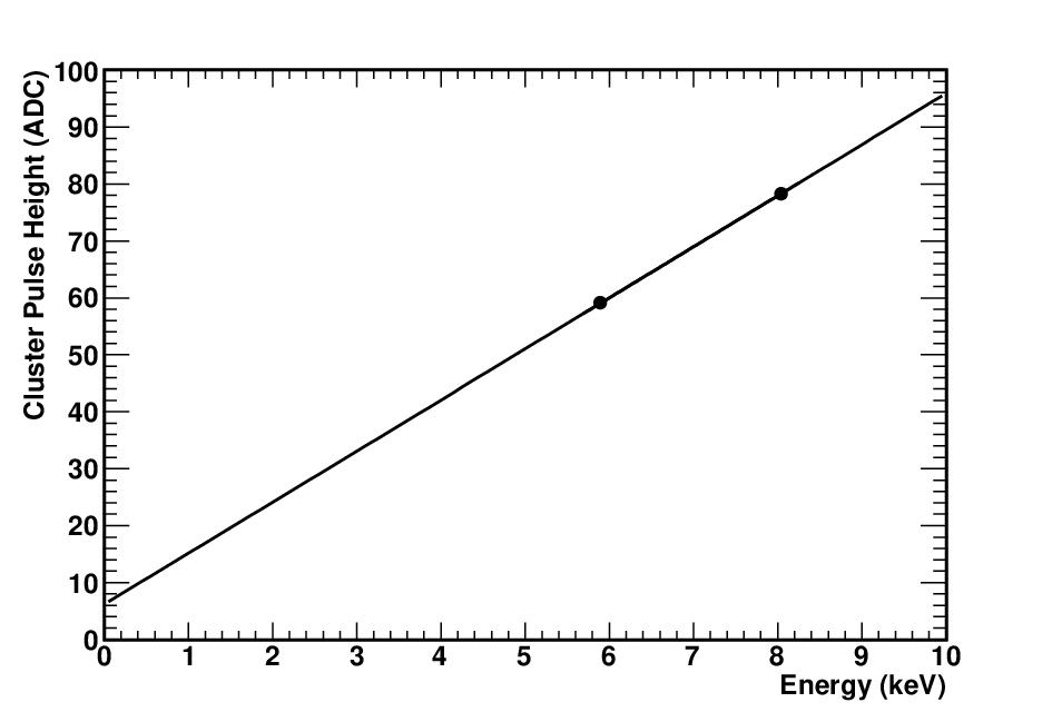
The ADC counts-to-electrons conversion is determined using the 5.9 keV X-rays emitted by a 55Fe source, which generate 1640 e-s in the sensor substrate. Pixels with floating -type guard-ring can be operated properly only up to = 20 V, since for higher voltages the back-gating effect sets in. This agrees with what already observed on previous sensor prototypes. Pixel cell designs with no -type guard-ring and BPW connected to the pixel diode show the best performances and are used in the rest of this study. These sectors are fully functional up to = 100 V and the signal for 5.9 keV X-ray conversion is clearly visible in the cluster pulse height spectrum. The pixel gain and noise are studied as a function of the depletion voltage for various clock frequencies and operating temperatures. We observe a decrease of the gain with increasing depletion voltage up to 50 V, when the gain becomes stable at 27.5 ADC count-1. The pixel cells with BPW below the transistors and connected to the diode exhibit full charge collection in the diode but 9% lower gain compared to those with the BPW layer only connected to the diode, possibly due to the increased cell capacitance. The pixel calibration is verified using 8.04 keV Cu-fluorescence X-rays from the data collected in a run at the ALS. Results are shown in Figure 2, which exhibits a linear scaling of the cluster pulse height with the X-ray energy.
 |
 |
A set of measurements to determine the current flowing in the detector substrate as a function of the depletion voltage are performed by biasing the chip and monitoring the current with a DC source/monitor unit. In this measurement the depletion voltage is applied to the probe station plate. Two probes are used to measure the currents in the chip. The first measures the current to the pixel guard-ring grid and the other that to the I/O implant, with the external guard-ring structure ( Outer) kept floating. The result is shown in Figure 3 with a comparison to the earlier sensor. The measured leakage current is of the order of 10-100 nA for 30 V. This result is in agreement with the calculation of the leakage current from the increase of the pixel dark levels for different integration times. The pixel noise is due in part to leakage current in the substrate. The SOImager-2 sensor shows a larger leakage current compared to the previous SOImager-1 prototype produced in the same process in 2008 (see Figure 3). The total single-pixel noise for 12.5 MHz read-out, measured in the lab and during the beam test, is (838) ENC at room temperature. After subtracting the read-out noise in quadrature, we obtain the detector single-pixel noise of (737) ENC at = 50 V and room temperature. It decreases to (434) ENC operating the sensor at -20∘C and it remains stable when varying the pixel clock frequency, , in the range 312.5 MHz.

4.2 Depletion depth, charge carrier signal and collection time
The measurement of the characteristics allows us to estimate the thickness of the depleted volume, provided the current in the substrate is not too large. The pixel guard-ring grid is used as electrode and the detector area is assimilated to a single large diode. For this measurement the guard-ring is kept at ground potential and the depletion voltage applied to the metallised back-side. Since the determination of the effective area used to derive the capacitance is affected by a large uncertainty, we use the measurement only for relative measurements. The solid line in the top panel of Figure 5 shows the depletion depth, relative to that at 50 V, inferred from the measured capacitance as a function of the applied substrate bias. When this measurement is repeated by applying to the biasing -type guard-ring, the result agrees.
The results from the C-V characteristics are compared to the evolution of the amount of charge collected as a function of the depletion voltage using 5.9 keV X-rays, 980 nm and 1060 nm wave-length laser pulses, and 200 GeV pions, which are virtually un-attenuated through the full detector thickness. Figure 4 shows the pulse height measured for clusters associated to a reconstructed track in the data collected with 200 GeV .

The evolution of the collected signal with the applied depletion voltage provides us with information on the thickness over which charge is collected in the pixel. If the charge is generated uniformly along the entire detector thickness, as in the case of the 1060 nm laser and the pions, we expect the measured signal to increase proportionally to , i.e. as the depleted thickness. On the contrary, if the penetration depth is smaller, the pulse height should reach a saturation level when the depleted thickness exceeds the penetration depth. Another estimator of the sensitive thickness is the rate of 55Fe X-rays clusters detected as a function of , which we expect to scale proportionally to the thickness of the sensitive region. We determine the most probable value of the cluster pulse height by performing a fit with a Gaussian curve to the laser data and with a Landau function folded with a Gaussian noise term for the pion data. Results are summarised in Figure 5, which shows the most probable value of the measured cluster pulse height for the 980 nm and 1060 nm laser and for the 200 GeV pions and the rate of 55Fe clusters, normalised to the values obtained for the reference value of = 50 V, as a function of the depletion voltage. We observe that the recorded pulse height increases, as expected, with the depletion voltage for both the pions and the 1060 nm laser. The scaling of the pulse height for clusters from laser pulses and pions is in remarkable agreement with that obtained from the characteristics curve, which scales as . The relative rate of 55Fe clusters also agrees with this scaling. Instead, for the 980 nm laser data we observe a saturation starting at 60 V.
 |
 |
Using the absorption coefficient in Si from [21], we compute the Si thickness in which 85 % of the charge carriers are generated to be (13025) m, where the quoted uncertainty represents the effect of a 15 % change in the value of the Si absorption constant, consistent with observations in [21]. We estimate the effective depleted thickness as a function of the depletion voltage, assuming that the measured signal scales as:
| (1) |
and perform a 1-par fit to extract the effective resistivity of the bulk Si from the pion data (see Figure 5). We obtain = (753 41) cm. This value would correspond to the real resistivity of the Si if all the collected charge were generated in the depleted layer, while we cannot exclude that the undepleted bulk also contributes to the detected signal. In any case, the fitted value is in reasonable agreement with the nominal resistivity of the SOI wafers of 700 cm, declared by the manufacturer. Using the fitted value of the resistivity we obtain an effective sensitive thickness of 115 m at =60 V.
Finally, we study the charge carrier collection time from the evolution of the signal on a pixel hit by a highly collimated laser pulse. To perform this measurement, a 2 ns-long pulse of a 980 nm laser is synchronised to shine the detector at the start of the 80 ns-long read-out window of the pixel onto which the pulse is focused. The analog signal is sampled at the pixel output using a 1 GHz digital oscilloscope. The time elapsing between the end of the laser pulse and the time at which the analog signal reaches a plateau is measured at various depletion voltages on the oscilloscope. We observe a decrease of this time interval with increasing values of until it stabilises at 17 ns for depletion voltages in excess of 40 V. This value does not necessarily reflect the real collection time since it could be due to the settling time of the read-out electronics, but demonstrates the effect of increasing electric field on the charge carriers. Figure 6 shows the observed analog signal trace and the average time interval obtained from a series of ten subsequent measurements as a function of , for sensor front illumination.
 |
 |
4.3 Signal sharing among pixels

Figure 7 shows the average multiplicity of the pixels in a cluster for 980 nm laser pulses and 5.9 keV X-rays as a function of the applied depletion voltage, . We observe that, although the charge spread decreases with , the signal remains distributed over multiple pixels also for large voltages.
 |
 |
Therefore, we study the charge sharing on neighbouring pixels as a function of the position of generation of carriers in the detector. This is usually characterised by the distribution defined as , where and denote the pulse height on the left and the right, respectively. Originally introduced in the characterisation of strip detectors [22], the definition of is extended to pixel detectors by summing the pixel charge over each column. The distributions obtained for 980 nm laser pulses and 200 GeV pions are shown in Figure 8. We observe a small variation of the distribution with using the 980 nm laser and no significant variation with energetic pions. This result seems to indicate that the charge sharing among neighbouring pixels is not dominated by the charge carrier cloud size and that, instead, the pixel capacitive coupling plays a significant role in determining the observed signal distribution.
5 Detector tracking performance
The detector tracking performance is studied using the the 200 GeV pion data and is characterised in terms of the detection efficiency, the single point resolution and the response to inclined tracks.
5.1 Detection efficiency
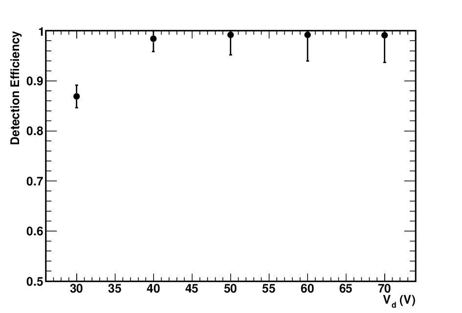
The detection efficiency is measured as the fraction of tracks reconstructed on the first layer of the doublet and on the singlet layer of the telescope, according to the criteria given above, which have a reconstructed hit on the second doublet layer within 10 m from the position of the track extrapolation. Figure 9 shows the detection efficiency as a function of . We observe a sharp rise, due to the increase of the signal S/N with from the increase of the sensitive thickness, up to 40 V. For larger voltage values, the detection efficiency stabilises at the value of 0.99, where the uncertainty is statistical.
5.2 Spatial resolution
The single point resolution is extracted from the Gaussian width of the residual distributions for reconstructed 200 GeV pion tracks. The residuals are defined as the differences between the reconstructed coordinate of the point of impact on the DUT and that extrapolated from the track reconstructed on the other two detector planes. Figure 10 shows the residual distributions obtained using alternatively the second plane of the doublet and the singlet plane as DUTs. The measured width of the residual distribution is the quadratic sum of the single point resolution of the DUT and the track extrapolation accuracy. This, in turn, depends on the single point resolution of the other planes. Since the three planes are all equipped with the same detectors, operating at the same depletion voltage, we assume they all have the same point resolution.
 |
 |
We use a Geant 4-based simulation to relate this single point resolution to the measured residual width. This includes the effects of multiple scattering, though they are small at the pion energy used in our tests, and hadronic interactions. Residuals are computed using both the second layer of the doublet, where the track extrapolation accuracy is higher, and the singlet, where the sensitivity to the point resolution is higher, as DUT. In computing the extrapolation resolution on the DUT,we assign an uncertainty of 0.5 mm on the longitudinal position of the doublet and 1.0 mm on that of the singlet layer. Results are summarised in Table 1 for various values of . For 50 V, the point resolution is measured to be (1.120.03) m, where the quoted uncertainty includes the statistical and the systematic uncertainties on the DUT longitudinal position.
| (V) | (m) | |
|---|---|---|
| Doublet | Singlet | |
| 30 | 1.430.06 | 1.300.06 |
| 40 | 1.180.03 | 1.120.05 |
| 50 | 1.140.03 | 1.020.06 |
| 60 | 1.150.07 | 1.100.08 |
| 70 | 1.080.06 | 1.050.07 |
5.3 Response to inclined tracks
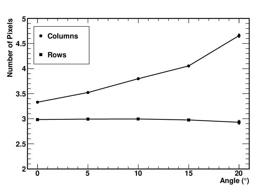
Finally, we study the cluster shape as a function of the angle between the incident pion track and the normal to the detector plane on the singlet plane of the telescope. The change of the cluster shape as a function of the angle of incidence is important for assessing the detector response to forward tracks in a vertex tracker with a barrel layout and to low momentum background particles [23]. In the beam test the angle of incidence is varied remotely by operating the rotation stage between 0∘ and 20∘. We take 200 GeV tracks which have associated hits on all three planes and characterise the cluster shape as the number of pixels along rows and columns in the cluster associated to the pion track on the third plane. Since the rotation axis is parallel to the pixel columns we expect to observe an increase of the multiplicity along the column and a constant average number of pixels along the rows. Figure 11 shows the average number of pixels along columns and rows in clusters on the third plane as a function of the detector angle.
6 Conclusions
A prototype pixel chip in OKI 0.20 m SOI technology with 13.75 m pixel pitch has been designed, processed and characterised in the laboratory with X-rays and short IR laser pulses and on a CERN SPS beam-line with 200 GeV . The use of a buried -well implanted beneath the buried oxide avoids the back-gating effect and the tested chip demonstrates for the first time large charge collection, high efficiency and micron resolution in a beam test. The chip can be properly operated to voltages 70 V, corresponding to an estimated thickness of the depleted region 125 m. We study the evolution of the collection time for the charge generated by a 980 nm laser in front illumination as a function of and measure collection times below 20 ns for 50 V. The hit reconstruction efficiency for high energy pions has been measured to be 0.99 and the single point resolution (1.120.03) m, for 50 V. These results are very encouraging for the further development of pixel sensors in SOI technology for applications demanding particle reconstruction with high spatial resolution and efficiency.
Acknowledgements
This work was supported by the Director, Office of Science, of the U.S. Department of Energy under Contract No.DE-AC02-05CH11231 and by INFN, Italy. We are grateful to Y. Arai for his effective collaboration in the SOIPIX activities. We acknowledge support from CERN for the beam test at the SPS. We are indebted to M. Tessaro for the detector doublet mounting, T.S. Kim and A. Onnela for the setup at the beam test and to A. Behrens and A. Froton for the detector alignment on the H4 beam-line. We are also thankful to N. Alster and N. Pozzobon for their contribution to the data taking at CERN.
References
- [1] R. Turchetta et al., Nucl. Instr. and Meth. A 458 (2001) 677.
- [2] L. Greiner et al., to appear on Nucl. Instr. and Meth. A, doi:10.1016/j.nima.2010.12.006.
- [3] R. De Masi et al., Nucl. Instr. and Meth. A 628 (2011) 296.
- [4] A.-C. Milazzo et al, Ultramicroscopy 104 (2005) 152.
- [5] G. Deptuch et al., Ultramicroscopy 107 (2007) 674.
- [6] M. Battaglia et al., Nucl. Instr. Meth. A 622, (2010) 669.
- [7] R. Barbier et al., Nucl. Instr. Meth. A 610, (2009) 54.
- [8] J. Marczewski et al., Nucl. Instr. and Meth. A 549 (2005) 112.
- [9] J. Marczewski et al., Nucl. Instr. and Meth. A 560 (2006) 26.
- [10] H. Niemiec et al., Nucl. Instr. and Meth. A 568 (2006) 153.
- [11] Y. Ikegami et al., Nucl. Instr. and Meth. A 579 (2007) 706.
- [12] T. Tsuboyama et al., Nucl. Instr. and Meth. A 582 (2007) 861.
- [13] M. Battaglia et al., Nucl. Instr. and Meth. A 583 (2007) 526 [arXiv:0709.4218 [physics.ins-det]].
- [14] Y. Arai et al., Nucl. Instr. and Meth. A 623 (2010) 197.
- [15] P. Giubilato et al., to appear on Nucl. Instr. and Meth. A, doi:10.1016/j.nima.2010.11.185.
- [16] M. Battaglia et al., Nucl. Instr. and Meth. A 611 (2009) 105.
- [17] R. Brun and F. Rademakers, Nucl. Instr. Meth. A 389 (1997) 81.
- [18] F. Gaede et al., in Proc. of Interlaken 2004, Computing in high energy physics and nuclear physics, Report CERN 2005-002, 471.
- [19] F. Gaede, Nucl. Instr. and Meth. A 559 (2006) 177.
- [20] M. Battaglia et al., Nucl. Instr. and Meth. A 593 (2008) 292 [arXiv:0805.1504 [physics.ins-det]].
- [21] H.A. Weakliem and D. Redfield, J. Appl. Phys. 50(3) (1979) 1491.
- [22] J. Straver et al., Nucl. Instr. and Meth. A 348 (1994) 485.
- [23] L. Maczewski et al., Nucl. Instr. and Meth. A 610 (2009) 640.