Semiclassical Boltzmann transport theory for graphene multilayers
Abstract
We calculate the conductivity of arbitrarily stacked multilayer graphene sheets within a relaxation time approximation, considering both short-range and long-range impurities. We theoretically investigate the feasibility of identifying the stacking order of these multilayers using transport measurements. For relatively clean samples, the conductivities of the various stacking configurations depend on the carrier density as a power-law for over two decades. This dependence arises from a low density decomposition of the multilayer band structure into a sum of chiral Hamiltonians. For dirty samples, the simple power-law relationship no longer holds. Nonetheless, identification of the number of layers and stacking sequence is still possible by careful comparison of experimental data to the results presented here.
pacs
72.80.Vp,73.23.-b,72.80.NgI Introduction
Enormous progress has been made in the five years since the first experiments demonstrated that charge carriers in single graphene sheets behave like massless Dirac fermions. Making and studying such single-atom thick carbon sheets is now routinely done using a wide variety of techniques. (For reviews, see Refs. 1, 2).
While the allure of manipulating single monoatomic sheets has understandably attracted most of the attention in this field, from a technological, or for that matter, fundamental point of view, the properties of few-layer-graphene sheets are equally attractive. Many of the methods used to make monolayer graphene, such as mechanical exfoliation of graphite, epitaxial growth from silicon carbide and chemical vapor deposition on metals, can be suitably adapted to make graphene stacks, with a controllable number of atomic layers. Many of the unusual properties of the Dirac Hamiltonian that are used to describe monolayer graphene, such as having chiral and ambipolar carriers, survive in these multilayers, so one might expect that these sheets would have high mobility and favorable carrier transport properties. As a result, multilayer graphene may play an important role in future electronic devices where its additional “layer” degree of freedom could be manipulated [3] to achieve desirable properties, such as the demonstrated gate-tunable band-gap in graphene bilayers. [4]
There has been experimental and theoretical work on the optical properties of graphene multilayers, as well as some very recent theoretical predictions on the phonon-scattering in these multilayers.[5] However, there has not been a systematic study of the low temperature transport properties of graphene multilayers. In anticipation of forthcoming experiments on these systems, we use both analytical and numerical methods to understand carrier transport in graphene multilayers.
The complication in studying multilayers is the coupling between the layers. The carrier transport in a single graphene sheet can be readily understood using the Dirac Hamiltonian, which is the low energy effective theory for -orbitals located on the vertices of a carbon honeycomb lattice. For multilayers, the additional coupling between orbitals on neighboring layers depends sensitively on many factors such as the distance between the layers and their relative orientation. For example, graphene bilayers with a twist angle between their respective primitive cells are predicted to largely act as decoupled sheets.[6, 7] For Bernal stacking (also called A-B stacking), on the other hand, half the carbon atoms in each hexagon of the top layer lie exactly over the center of a hexagon of the layer below it. The resulting strong coupling between the two layers gives a low energy effective theory with a zero-gap hyperbolic dispersion.
While height fluctuations (or equivalently, having spatial fluctuations in the interlayer coupling strength), or allowing for arbitrary rotations and slips between the layers are important for some systems (such as epitaxial graphene), their effects are beyond the scope of the present work.[8, 9] Here we consider multilayers that come in families where the orientation of the upper layers is determined by symmetry considerations from the orientation of the bottom layer. This would be the case, for example, if the multilayer inherits its structure from a parent structure, as is the case in the mechanical exfoliation technique.
We further restrict our multilayer analysis to the lower energy stacking sequences in which neighboring layers share only one sublattice. For example, we consider bilayer graphene that is A-B stacked, where the two layers share one sublattice, but not A-A stacked, where each carbon atom of the top layer lies exactly on top of a carbon atom of the bottom layer (sharing both sublattices). The consecutive A-A stacking is energetically unfavorable,[10] so we do not consider this stacking and its generalization in multilayer stacks. For trilayer graphene, we consider two possibilities: A-B-A stacking (also called Bernal-like) is a Bernal bilayer, with the third layer having carbon atoms located directly above the bottom layer; and A-B-C stacking.
Figure 1 illustrates the different stacking sequences graphically. Since the honeycomb lattice of a single graphene sheet comprises two interpenetrating triangular sublattices, we label the sublattices of each layer and . When a subsequent graphene layer is placed on top of the stack, we consider the stacking orders where either the atoms of the or the sublattices are displaced along the edges of the honeycomb of this top sheet. This gives a stacking rule that implies three distinct but equivalent projections (labeled A, B, and C) of the three-dimensional structure’s honeycomb-lattice layers onto the - plane and consequently distinct stacking sequences for an -layer stack.
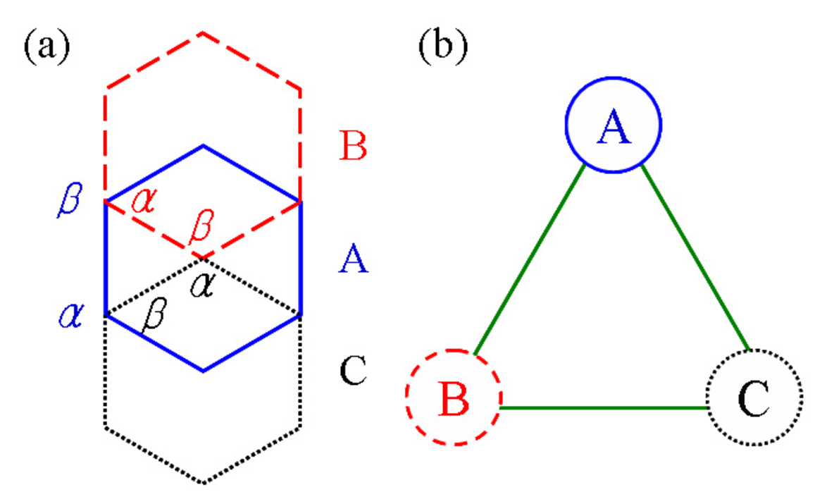
The electronic properties of multilayer graphene strongly depend on the stacking sequence. Periodically stacked multilayer graphene [11, 12] and arbitrarily stacked multilayer graphene [13] have been studied theoretically, demonstrating that the low-energy band structure of a graphene multilayer consists of a set of independent pseudospin doublets. It was shown that an energy gap can be induced by a perpendicular external electric field in ABC-stacked multilayer graphene.[14, 15] Furthermore, in ABC stacking, electron-electron interactions play a more important role than other stacking sequences due to the appearance of relatively flat bands near the Fermi level.[15] This enhanced role of electron interactions raises the likelihood of strongly-correlated ground-states, a possibility that we ignore in our semiclassical treatment below. Optical properties of multilayer graphene using absorption spectroscopy have been studied experimentally [16] and theoretically [17, 18] showing characteristic peak positions in optical conductivity depending on the stacking sequence.
Transport properties of monolayer, bilayer and multilayer graphene have been studied theoretically[19, 20, 21, 22] within coherent potential approximations. These approaches capture the scattering properties of the impurity potential (which is important for strong disorder), but they are often restricted to small system sizes, and do not accurately account for the disorder-induced spatial inhomogeneity of the fluctuating local carrier density. We believe this inhomogeneity dominates the transport properties of these graphene multilayers (see discussion in Ref. 2).
Our main finding is that for relatively clean samples, the carrier density dependence of the multilayer conductivity follows a power-law dependence for more than two decades, a direct consequence of the effective low energy chiral decomposition. For dirty samples, the carrier density inhomogeneity induced by the disorder washes away this power-law relationship. However, the various stacking sequences give characteristically different dependence of the multilayer conductivity on carrier density. By careful comparison with experimental data, our results could be used to identify both the number of layers and the stacking sequence of a multilayer graphene sample.
The rest of this manuscript is organized as follows. In Sec. II, we describe the theoretical model where we solve for the multilayer graphene band structure using a tight-binding model that includes both the nearest-neighbor intralayer hopping and the nearest-neighbor interlayer hopping, and solving for the conductivity within the Boltzmann transport formalism. In Sec. III we present our results for graphene stacks comprising one, two, three and four layers, treating impurity scattering by both Coulomb potentials and short-range disorder. In the appendices we present details of the chiral decomposition and the transport properties of -chiral fermions, as well as analytic results for the electronic transport in bilayer graphene.
II Theoretical model
II.1 Tight binding Hamiltonian
The low energy effective Hamiltonian for the -orbital continuum model for arbitrarily stacked -layer graphene centered at the hexagonal corners of the Brillouin zone is given by [23, 24]
| (1) |
where and is an electron annihilation operator for layer , sublattice and momentum measured from or point.
The simplest model for a multilayer graphene system allows only nearest-neighbor intralayer hopping and the nearest-neighbor interlayer hopping . The in-plane Fermi velocity for monolayer graphene, , is related to by , where nm is the lattice constant of monolayer graphene. This model ignores some aspects of the electronic band structure – in principle, corrections to this model, such as adding next-nearest-neighbor hopping, can easily be included, although in practice, it is often numerically quite intensive. We find that such corrections do not significantly alter any of our main findings.
II.2 Boltzmann transport theory
The conductivity is a property of electrons close to the Fermi energy and is obtained from the Einstein relation, where is the density of states at the Fermi energy and is the diffusion constant. In cases in which the Fermi surface has multiple sheets (lines in the two dimensional cases we consider here), the conductivity is the sum over such contributions for each sheet. See Sec. II.4 for details. For convenience, we denote the density of states for each sheet as where and are spin and valley degeneracy factors. For diffusive transport in two dimensions, . The Fermi velocity, density of states and relaxation time can be calculated from the dispersion relation as
| (2a) | |||
| (2b) | |||
| (2c) | |||
| where is the squared effective impurity scattering potential averaged over the angle, and the Fermi wavevector is related to the carrier density and applied back gate voltage . When the Fermi surface has multiple sheets, the left hand side of this last relation should be summed over for each sheet. The validity of the Born approximation implicit in this formulation is discussed in Appendix A, and the special case of -chiral fermions is treated in Appendix B. | |||
The scattering matrix element that gives rise to the transport relaxation time is obtained using the Boltzmann transport formalism
| (3) |
where is the matrix element of the impurity potential at scattering angle , and is the chirality factor that arises from the projection of the spinor wavefunctions between the incoming and outgoing states. For the case of intervalley and interband scattering, the treatment of the chirality factor is more subtle and discussed in Appendix C. For convenience, we define the dimensionless potential
| (4) |
where is the dielectric constant and is the effective fine structure constant. The conductivity can then be written as
| (5) |
where is the carrier density, and all the information about the band structure and the nature of the disorder potential is captured by and . When several bands cross the Fermi energy, we calculate and (which yields ) for each of the bands and then calculate the total conductivity as , where the applied gate voltage is proportional to , and is fixed by keeping the same for all bands.
II.3 Impurity Scattering
Different types of impurity potentials give qualitatively different results for the conductivity. This can be seen in Eq. 5, where the wavevector dependence of the Fourier transform of the impurity potential changes the scaling of the conductivity . Studies on monolayer graphene have explored a wide variety of disorder potentials including long-range Coulomb (), Gaussian-white noise () and Gaussian-correlated disorder () as well as resonant scatterers that cause a maximal phase shift of between incoming and outgoing wavefunctions. We refer to Ref. 2 for more details on the different kinds of disorder in graphene.
For our purposes, we focus on what we believe to be the most relevant scattering mechanisms, i.e. charged impurities (which act as screened long-range Coulomb disorder) and short-range defects (approximated as white-noise disorder). Using the Thomas-Fermi screening theory, one can write expressions for the dimensionless scattering potential which was defined in Eq. 4. For screened charged impurities from with we find
| (6) |
where the dimensionless Thomas-Fermi wavevector is and is the distance between the impurities and the graphene sheet. When several bands cross the Fermi energy, the Thomas-Fermi screening wavevector determined from the total density of states including all the bands. The monolayer Fermi velocity was defined below Eq. 1.
II.4 Intervalley and Interband Contributions
At typical carrier densities, the band structure of monolayer graphene comprises two Dirac cones that are centered at two inequivalent points (also called valleys) of the Brillouin zone boundary labeled as and . The scattering of carriers between the valleys requires a momentum transfer of , and is strongly suppressed for Coulomb impurities. For short-range scattering, the treatment depends on how one models the intervalley scattering matrix element, but in most cases it is sufficient to consider a single valley with a suitably defined impurity concentration (see e.g. Ref. 25). For concreteness, we assume that for short-range impurities, the intervalley and intravalley scattering matrix elements are equal, that is the average impurity concentration in a single valley (and is the same for both valleys). The conductivity using these definitions is smaller by a factor of 2 from the case of , where and are concentration of impurities or defects on the A and B sublattices, respectively.
As discussed in Appendix B, within a single valley, all finite stackings that are a subsequence of periodic ABC stacking; i.e. A, AB, ABC, ABCA, etc.; have only a single band at low energies, and the chirality increases as the number of layers increases. However, for other stackings, the band structure features multiple chiral bands with different dispersion relations that are centered at the Dirac point. For Coulomb impurities, the matrix element in Eq. 6 can be computed for both intraband and interband scattering, and their scattering rates added in accordance with Matthiessen’s rule. For short-range impurities, the interband scattering is more subtle. A straightforward application of Eq. 7 would lead to a strong suppression of all interband scattering because the chirality factor vanishes or is significantly less than one. As discussed in Appendix C we believe this to be unphysical because it requires the short-range impurity potential to be diagonal in the space of all the layer and valley quantum numbers. Most short range scatters we can imagine would be localized to one layer and a specific sublattice so the scattering potential would not be diagonal in this space. The screened Coulomb potential, on the other hand, varies slowly between the layers and sublattices and can be much better approximated as diagonal in that space. In the absence of a microscopic model for a particular impurity model (e.g. computing the scattering potential resulting from a single vacancy or from the binding of a single hydrogen atom to the top layer), we believe that for short range scatterers, a more realistic assumption is to set . This correctly weights the relative importance of intraband and interband scattering, and therefore gives the correct qualitative carrier density dependence of the conductivity.
The role of interband scattering is most striking when one considers the large density regime where higher energy bands become accessible. For screened charged impurities, the additional density of states in these higher energy bands enhance the screening of long-range impurities which will sharply increase the conductivity, while the interband scattering is suppressed by the chirality factor. On the other hand, for short-range impurities, the higher energy band becomes an additional source of interband scattering that sharply decreases the conductivity. At the time of writing, there have been no transport experiments that could probe these higher energy bands by inducing sufficiently large carrier densities. However, if such an experiment is done in the future (perhaps by finding better electrolytes), then the increase (decrease) of would be indicative of Coulomb (short-range) impurities being the dominant source of scattering.
II.5 Effective Medium Theory (EMT)
At low carrier density, the disorder induced fluctuations in the local density become larger than the spatially averaged carrier density. This has been called the electron-hole puddle regime. We use the effective medium approach developed in Ref. 26 to obtain the bulk conductivity of this inhomogeneous medium. It was shown in Ref. 27 that by assuming a Gaussian probability distribution for the carrier density, could be obtained from using
| (8) |
where parameterizes the Gaussian distribution, and is obtained numerically from Eq. 5. This integral equation extrapolates from for to for . The effect of the puddles, therefore, is to give rise to a minimum conductivity plateau where the conductivity remains roughly constant when the average of the carrier density is smaller than its fluctuations.[28]
III Results and Discussion
As outlined above, for an arbitrary graphene stack we first solve Eq. 1 to obtain the band structure. For simplicity, we choose eV, eV, and . Neglecting higher order hopping terms keeps the spectrum rotationally symmetric (reducing the computational time), while the ratio of is a number of order unity that can be calculated within the low-density chiral decomposition (see Appendix B). We do not believe that these approximations significantly alter our findings.
Having solved numerically for the wavefunctions, one can compute (Eq. 2a), (Eq. 2b), as well as the chirality factor (see Appendix C). For the short-range and Coulomb disorder potential we use representative [29] parameters: nm and nm. Equation 8 then gives the predicted carrier density dependence of the conductivity.
 |
 |
 |
 |
Figure 2 shows the results for short-range scatterers such as point defects. The left panel (Fig. 2a and Fig. 2b) assumes a relatively clean sample with . The solid lines are calculated from Eq. 8, while dashed lines show the (approximate) power-law dependence of the conductivity on carrier density. We find that for most cases the conductivity limited by short-range scatterers exhibits a unique power-law (for more than two decades) that depends on the number of layers and the stacking sequence. For such clean samples, where the scattering is dominated by short-range disorder, with the exception of the similarity between AB bilayers and ABA trilayers, the distinct power-law dependence for enables easy identification of the sample from transport measurements.
The right panel (Fig. 2c and Fig. 2d) shows the results for a dirty sample (). The solid lines show the EMT result (Eq. 8) and the dashed lines show the Boltzmann result before the EMT averaging (Eq. 5). We note that the results for monolayer and bilayer graphene agree with analytical calculations discussed in Appendix D. While there is no simple power-law dependence of the conductivity on carrier density, the different stacking sequences have very different functional forms for . (For example, the ratio varies by almost an order of magnitude). It might therefore still be possible to identify the number of layers and the stacking sequence from transport.
 |
 |
 |
 |
The results for charged impurities is shown in Fig. 3. Again the left panel shows a clean sample (). While all the different stacking sequences have a power-law dependence for , unfortunately, with the exception of ABA and ABCB, the rest are all very close to a linear dependence. It would therefore be difficult to distinguish the samples in any transport measurement in the low carrier density regime (i.e. ). For a dirty sample with a larger range of carrier density (), we find that the functional forms for are sufficiently different. We emphasize that the figures show the conductivity on a log-log scale. Different slopes correspond to different scaling exponents , where . For example, as seen in Fig. 3d, while the different stackings of the tetralayer have similar values for the conductivity at , the minimum conductivity for the ABCB tetralayer is two orders of magnitude larger than the ABCA stacking.
To further understand these results, we note that the transport properties of graphene multilayers are determined by two characteristic densities: the band density where , and the impurity density . By gating graphene, one can change both the carrier density and the type of carriers, where a negative back-gate voltage induces holes, and a positive back-gate induces electrons. With special dielectrics one can induce carrier densities as large as (see Ref. 30), although typically carrier densities do not exceed .
For carrier densities much lower than the characteristic band density , one can decompose the electronic structure of an arbitrary multilayer into parallel channels of bands, each with the simple dispersion relation where is the chirality index. The number of channels and the chirality index are determined from the stacking sequence as discussed in Ref. 31. More details on the wave-functions and transport of -chiral fermions can be found in Appendix B.
In the opposite limit of , the band structure of -layer graphene decomposes into that of decoupled monolayer graphene sheets, irrespective of the stacking sequence. Since the transport of monolayer graphene has been well studied (see Ref. 2), we do not explore this limit in any detail. Although we note, that even at the extremely large carrier density , one is not yet in the limit of essentially decoupled sheets.
The second important scale is that of disorder. Typical values of vary from (in suspended graphene) to . Only when the carrier density is much larger than can one use the usual semi-classical Boltzmann transport theory. When , the inhomogeneous landscape of electron and hole puddles gives rise to a saturation in the conductivity approaching a finite at the Dirac point.
One can immediately identify two regimes that are experimentally relevant. When , one can exploit the chiral decomposition to obtain a power-law dependence of the conductivity on carrier density. This is what we called the “clean sample” regime (the left panels of Fig. 2 and Fig. 3). In Appendix B we derive the Effective Medium conductivity for arbitrary -chiral fermions, and we can use this decomposition to understand our results.
As an example, consider the clean ABC stacked trilayer. As seen in Fig. 2, for short-range impurities. This dependence follows directly from the low energy chiral decomposition discussed in Appendix B where the ABC trilayer is approximated by a chiral system, and (see Eq. B). Similarly, the numerical results for the ABC stacked trilayer with charged impurities shown in Fig. 3 is quite close to the expected power-law . This small difference between the numerical results and those anticipated from the chiral decomposition is the result of our using a finite for the distance of the Coulomb impurities from the graphene sheet. The finite softens the small-distance divergence of the Coulomb potential, thereby increasing the conductivity and giving a larger coefficient for the (approximate) power-law .
A similar analysis can be done for the ABA stacked trilayer graphene. At low energies, it is described by a direct product of and chiral systems. At low density, the band structure has two sheets, one with a linear dispersion like monolayer graphene, and one with a parabolic dispersion similar to bilayer graphene. Requiring a constant Fermi energy, one can introduce a dimensionless parameter . The chiral decomposition is valid when . One notes that where the effective Fermi velocity is shown in Table 1. This implies that at low carrier density where the chiral decomposition is valid, the band with the larger chirality also has a larger carrier density and larger density of states. In the case of ABA trilayers, this implies that for short-range scatterers, it behaves exactly like the AB bilayer which is also a chiral system and (as seen in Fig. 2a). For charged impurities, the large density of states from the band effectively screens the impurities so that the band behaves like monolayer graphene with short-range impurities having constant. All the shown power laws in left panels of Fig. 2 and Fig. 3 can be understood in this manner using the chiral decomposition.
The second regime relevant to experiments is when . We called this the “dirty sample” regime, since having a cleaner sample offers no qualitative difference. The important point is that since , the chiral decomposition is not valid, and the band-structure has no simple analytical form. This regime can be seen in the right panels of Fig. 2 and Fig. 3. Although no simple analytical expression or power-law behavior determines , the results for the different number of layers, the different stacking orders and short-range vs. long-range impurities are all sufficiently different. Therefore, by comparison of experimental data to the results presented here, it should be possible to identify not only the number of layers and stacking sequence, but also the nature of the dominant source of disorder.
IV Conclusion
We have considered the transport properties of multilayer graphene stacks. The formalism is quite general and can be used for -layers of graphene with arbitrary stacking between the layers. In the absence of any experimental data for layers with , we have considered the most energetically favorable stacking sequences and the cases of both short-range and long-range impurities. For monolayer and bilayer graphene, our results agree with previously known results (see Appendix D). For trilayer graphene, we show that ABA and ABC stacking have very different transport properties and can be distinguished from each other. Similarly, for tetralayer graphene, ABCA, ABCB and ABAB each is a separate electronic material with its own characteristic dependence of conductivity on carrier density. (The ABCB and ABAC stackings have the same conductivity since they are related to each other by a symmetry transformation.)
An important objective of this work is to enable experimentalists working on multilayer graphene to be able to use transport measurements to identify and characterize their multilayer samples. In addition, one could use our results to determine the nature of the dominant impurity potential,[32] the effect of changing the dielectric environment [29] or identify when other effects (such as quantum interference[33]) that we have neglected in our semi-classical approach become important.
Information from transport measurements could be used in conjunction with other techniques such as Raman spectroscopy [34], optical detection [18] and observing the scattering from phonons at high temperature. [5] Our main finding is that in most cases, the different stacking sequences have different electronic properties that result in characteristic dependence of the conductivity on the applied carrier density.
Acknowledgements.
The authors thank E. H. Hwang for valuable comments. This work was supported in part by the NIST-CNST/UMD-NanoCenter Cooperative Agreement.Appendix A Validity of the Born approximation
In this work, we use the Born approximation for both short-range and Coulomb impurities as seen explicitly in Eq. 7. This approximation is valid if the scattering potential is weak enough. As the scattering potential becomes stronger, the scattering approaches the unitary limit, in which the scattering amplitude becomes independent of the strength of the potential. In the unitary limit, the strength of the impurity potential drops out of the expression for the conductivity, which then depends only on the impurity concentration [35]
| (9) |
where characterizes the range of the potential. [36] In the opposite limit of weak scatterers, the strength of the impurity potential determines the conductivity. For consistency with the notation in Ref. 35, we introduce a scattering potential in Eq. 2c so that Eq. 5 reads
| (10) |
In the Born limit, it is the product that determines the conductivity.
Ultimately, microscopic models of measured defects will determine whether the scattering is better described by the unitary limit or the Born limit. In the absence of such a model, an important issue for our results is whether the combination of conductivities and carrier densities we consider require that the scattering potential be so strong that the Born approximation is no longer valid. In a recent article, Ferreira et al.[35] test the validity of the Born approximation by computing the scattering amplitude as a function of the scattering potential strength for short-range impurity scattering in monolayer and bilayer graphene. For weak scattering potentials, the Born approximation results agree with their more general calculations but for large enough potentials, the scattering amplitude reaches the unitary limit where the scattering phase-shift is irrespective of the strength of the impurity potential. We use their results to argue that the conductivities and charge densities we treat are consistent with the Born approximation being valid.
As discussed by Ferreira et al. the validity of the Born approximation depends on the quantity . If , we have the unitary limit, and if we are in the Born limit. To check the self-consistency of the Born approximation limit, we can re-write this condition as
| (11) | |||||
where we assume . A similar expression is obtained for bilayer graphene with the prefactor replaced by . The Born approximation is valid for a relatively high density of relatively weak scatterers. Since (both experimentally, and for the validity of the diffusive approximation, see Ref. 33), and typical carrier densities range from to , the Born approximation provides a consistent solution when there are no fewer than one short-range impurity per (or more than one defect per 2000 carbon atoms). These numbers seem quite reasonable, given the preparation method of these samples. In Ref. 29 the authors measured for monolayer graphene, giving two orders of magnitude wider range of carrier densities for the validity of the Born approximation for the same impurity concentration. Similarly, in Fig. 2a although we take in order to illustrate the power law dependence of the conductivity due to the chiral decomposition, the Born approximation is still valid because we also take to be much larger. While such arguments do not rule out the possibility that the scatterers are in the unitary limit, they nonetheless establish the Born approximation treatment is self-consistent.
Appendix B Conductivity of -chiral Fermions
At very low carrier density, an arbitrarily stacked graphene multilayer can be described as a superposition of pseudospin doublets. This decomposition holds so long as , where is the chirality index for the pseudospin doublet.
The rules for the decomposition are as follows: (monolayer graphene) A; (bilayer graphene) AB; (trilayer graphene) ABA and ABC . This notation indicates, for example, that an ABC stacked trilayer is described by a -chiral Hamiltonian, while an ABA stacked trilayer is composed of two bands – one similar to monolayer graphene and the second similar to bilayer graphene (see Table 1 and Refs. 31, 37, 38 for more details). The -chiral Hamiltonian is defined as
| (12) |
where and is the effective in-plane Fermi velocity (for example, for monolayer graphene and bilayer graphene, and in general for periodic ABC stacking).
Throughout the manuscript we have used the following properties of the energy levels and wavefunctions for the -chiral system
| (13) | |||||
The band-index corresponds to the positive (negative) energy states of the conduction (valence) band and . The intraband chirality factor is then calculated as
| (17) |
The scaling of the conductivity with carrier density can be immediately obtained by noticing that and . This gives
| (18) |
which depends on the scattering potential . Assuming for simplicity and restoring the dimensions, we find
| Number of layers (N) | Stacking sequence | Chirality (J) | Effective velocity |
|---|---|---|---|
| 1 | A | 1 | |
| 2 | AB | 2 | |
| 3 | ABA | 12 | |
| 3 | ABC | 3 | |
| 4 | ABAB | 22 | |
| 4 | ABCA | 4 | |
| 4 | ABCB | 13 | |
| 4 | ABAC | 13 |
where for , for and for , while for in Eq. (17) and for . (Here we are considering a -chiral system in Eq. 12 and did not include intervalley scatterings.) The result for the bare Coulomb potential was presented in Eq. B for a pedagogical reasons, and case for the bare and screened Coulomb potentials was also considered for completeness. We note that since
| (23) |
for the low density limit , the overscreened Coulomb potential becomes a good approximation for charged impurities. In this low density limit, among the short-range scattering and screened Coulomb scattering, screened Coulomb scattering dominates over short-range scattering for , (with a corresponding ); while short-range scatterers dominate for (and ). (Note that because of the Matthiessen’s rule, a scattering mechanism with smaller conductivity dominates.) Bilayer graphene at low carrier density (or ) is unique in that both charged impurities and short-range disorder give conductivities with the same carrier density dependence [39, 40, 41] making them difficult to distinguish experimentally.[32] In the opposite limit of very high carrier density, the energy band structure of multilayer graphene separates into a collection of decoupled monolayer graphene bands.[18] As a result, the conductivity scales as that of a monolayer at very high carrier density.
As discussed above, the chiral decomposition works only at low carrier density where it is known that density fluctuations dominate the transport properties.[42, 28, 26] One must therefore estimate whether there is a regime of validity where the carrier density is large enough so that the puddle physics no longer dominates (i.e. ), but small enough that the chiral decomposition is still valid (i.e. ); here is the root-mean-square fluctuation in carrier density induced by the disorder potential, while is the crossover density scale. We estimate using the self-consistent approximation of Refs. 28 and 39, where , and is the disorder potential of screened charged impurities located at some distance from the graphene sheet
| (24) | |||||
For the relevant limit , (for details, see Ref. 28). Although we used a charged impurity model for the disorder potential, in this limit the impurities are perfectly screened, and the long-range nature of the impurity becomes irrelevant (i.e. one gets similar results starting from a short-range impurity model). Assuming a Gaussian probability distribution for the carrier density, we find that for the -chiral Hamiltonian (with )
| (25) |
which shows that for any given , one can determine the minimum disorder concentration necessary to ensure that . (The factor of 3 inside the square-root is added to conform to the convention for graphene monolayers, see Ref. 2.) Note that for monolayer graphene, one has to use the full dielectric function for the screening.[28]


From Eqs. 8 and B one can easily construct an Effective Medium Theory for the -chiral model. The conductivity is obtained by solving the integral equation
| (26) |
To illustrate the differences between different -chiral models, in Fig. 4 we show for and assuming short-range disorder, where we estimate from Eq. 25 assuming that and . As seen in the figure, the electron and hole puddles tends to pin the conductivity value close to its minimum value, and that the puddle regime increases with increasing .
Appendix C Chirality factor for intervalley and interband scattering
It is often argued that monolayer graphene has a high mobility because the chiral nature of carriers prevents backscattering. In the diffusive regime, the scattering rate involves an integral of the chirality factor over all angles weighted by the Boltzmann factor . As discussed in Ref. 39, the enhancement due to chirality is no more than a factor of order unity. Similarly for graphene multilayers, one can calculate numerically, and illustrative examples are shown in Fig. 5 for the ABA trilayer and ABCB tetralayer. For intraband scattering and at low density, the chirality factor agrees with the analytic results in Eq. 17 derived for -chiral Hamiltonians. For the range of carrier densities we consider, the chirality factor changes the conductivity by a factor of order unity, just like the case of monolayer graphene. However, a similar calculation of the interband chirality factor shows quite different results. Figure 5 shows that the interband chirality factor is exactly zero for the ABA trilayer and strongly suppressed for the ABCB tetralayer.
It can be shown that the interband chirality factor in all periodic AB stackings vanishes from the form of the wavefunctions [37], and in all other layer stackings it is strongly suppressed compared with the intraband chiral factor. At first glance, this might suggest that interband scattering is negligible and can be ignored. However, we point out that being able to decompose the scattering matrix element into a plane-wave-like overlap and a chirality factor as we did in Eq. 3 relies on the impurity potential being diagonal in the chiral-basis for graphene layers with 2 valleys. This might be a reasonable assumption for the potential of remote charged impurities located at nm to 2 nm away, but not for vacancies or adsorbates that would be strongly localized on one of the layers. Without a microscopic theory that would give the matrix structure of the impurity potential in this chiral basis (and we note that such a theory would likely be non-universal depending strongly on the type of defect), it is more reasonable to set for short-range impurities. For generic short-ranged disorder, this would correctly weight the relative importance of the interband and intraband contributions at the expense of losing the chirality enhancement factor of order unity. Since we are interested in quantities such as the power-law trends for (left panels of Fig. 2 and Fig. 3) or the ratio between at high and low carrier density (right panels of Fig. 2 and Fig. 3), this approximation is well suited to the scope of this work.


Appendix D Bilayer graphene: Analytical results
In this section we derive analytic results for the transport properties of bilayer graphene. The bilayer graphene Hamiltonian is
| (27) |
where and energy eigenvalues and eigenvectors (up to normalization) are
| (28) |
where
| (47) | |||||
From Eq. 5 taking into account only the low energy band with the energy , the Fermi velocity is given by
| (48) |
and the density of states per spin and valley at the Fermi energy is
| (49) |
The chirality factor within the same band is given by [32]
| (50) | |||||
where , , and .
For simplicity, let’s consider the conductivity when the Fermi energy crosses only the low energy band . For short-range disorder, from Eq. 7
| (51) |
where with the chirality factor of Eq. 50, while for . Then, we find
| (52) |
Note that if we include the intervalley scattering, the conductivity becomes smaller by a factor of 2.
References
- [1] A. H. Castro Neto, F. Guinea, N. M. R. Peres, K. S. Novoselov, and A. K. Geim, Rev. Mod. Phys. 81, 109 (2009).
- [2] S. Das Sarma, S. Adam, E. H. Hwang, and E. Rossi, Rev. Mod. Phys. (in press); arXiv:1003.4731 (2011).
- [3] A. A. Avetisyan, B. Partoens, and F. M. Peeters, Phys. Rev. B 81, 115432 (2010).
- [4] Y. Zhang, T.-T. Tang, C. Girit, Z. Hao, M. C. Martin, A. Zettl, M. F. Crommie, Y. R. Shen, and F. Wang, Nature 459, 820 (2009).
- [5] H. Min, E. H. Hwang, and S. Das Sarma, arXiv:1011.0741 (2010).
- [6] J. Hass, F. Varchon, J. E. Millán-Otoya, M. Sprinkle, N. Sharma, W. A. de Heer, C. Berger, P. N. First, L. Magaud, and E. H. Conrad, Phys. Rev. Lett. 100, 125504 (2008).
- [7] J. M. B. Lopes dos Santos, N. M. R. Peres, and A. H. Castro Neto, Phys. Rev. Lett. 99, 256802 (2007).
- [8] E. J. Mele, Phys. Rev. B 81, 161405 (2010).
- [9] R. Bistritzer and A. H. MacDonald, Phys. Rev. B 81, 245412 (2010).
- [10] J.-C. Charlier, J.-P. Michenaud, and X. Gonze, Phys. Rev. B 46, 4531 (1992).
- [11] S. Latil and L. Henrard, Phys. Rev. Lett. 97, 036803 (2006).
- [12] F. Guinea, A. H. Castro Neto, and N. M. R. Peres, Phys. Rev. B 73, 245426 (2006).
- [13] H. Min, R. Bistritzer, J. Su, and A. H. MacDonald, Phys. Rev. B 78, 121401 (2008).
- [14] M. Aoki and H. Amawashi, Solid State Communications 142, 123 (2007).
- [15] F. Zhang, B. Sahu, H. Min, and A. H. MacDonald, Phys. Rev. B 82, 035409 (2010).
- [16] K. F. Mak, J. Shan, and T. F. Heinz, Phys. Rev. Lett. 104, 176404 (2010).
- [17] M. Koshino and T. Ando, Solid State Communications 149, 1123 (2009), ISSN 0038-1098.
- [18] H. Min and A. H. MacDonald, Phys. Rev. Lett. 103, 067402 (2009).
- [19] J. Nilsson, A. Castro Neto, N. Peres, and F. Guinea, Phys. Rev. B 73, 214418 (2006).
- [20] J. Nilsson and A. Castro Neto, Phys. Rev. Lett. 98, 126801 (2007).
- [21] J. Nilsson, A. H. Castro Neto, F. Guinea, and N. M. R. Peres, Phys. Rev. B 78, 045405 (2008).
- [22] S. Yuan, H. de Raedt, and M. I. Katsnelson, arXiv:1010.2858 (2010).
- [23] B. Partoens and F. Peeters, Phys. Rev. B 74, 075404 (2006).
- [24] B. Partoens and F. M. Peeters, Phys. Rev. B 75, 193402 (2007).
- [25] N. Shon and T. Ando, J. Phys. Soc. Jpn. 67, 2421 (1998).
- [26] E. Rossi, S. Adam, and S. Das Sarma, Phys. Rev. B 79, 245423 (2009).
- [27] S. Adam and M. D. Stiles, Phys. Rev. B 82, 075423 (2010).
- [28] S. Adam, E. H. Hwang, V. M. Galitski, and S. Das Sarma, Proc. Natl. Acad. Sci. USA 104, 18392 (2007).
- [29] C. Jang, S. Adam, J.-H. Chen, E. D. Williams, S. Das Sarma, and M. S. Fuhrer, Phys. Rev. Lett. 101, 146805 (2008).
- [30] D. K. Efetov and P. Kim, Phys. Rev. Lett. 105, 256805 (2010).
- [31] H. Min and A. H. MacDonald, Phys. Rev. B 77, 155416 (2008a).
- [32] S. Xiao, J.-H. Chen, S. Adam, E. D. Williams, and M. S. Fuhrer, Phys. Rev. B 82, 041406 (2010).
- [33] S. Adam, P. W. Brouwer, and S. Das Sarma, Phys. Rev. B 79, 201404 (2009).
- [34] A. C. Ferrari, J. C. Meyer, V. Scardaci, C. Casiraghi, M. Lazzeri, F. Mauri, S. Piscanec, D. Jiang, K. S. Novoselov, S. Roth, et al., Phys. Rev. Lett. 97, 187401 (2006).
- [35] A. Ferreira, J. V. Gomes, J. Nilsson, E. R. Mucciolo, N. M. R. Peres, and A. H. Castro Neto, arXiv:1010.4026v1 (2010).
- [36] T. Stauber, N. M. R. Peres, and F. Guinea, Phys. Rev. B 76, 205423 (2007).
- [37] H. Min and A. H. MacDonald, Prog. Theor. Phys. Suppl. 176, 227 (2008b).
- [38] M. Koshino and E. McCann, Phys. Rev. B 81, 115315 (2010).
- [39] S. Adam and S. Das Sarma, Phys. Rev. B 77, 115436 (2008).
- [40] M. Katsnelson, Phys. Rev. B 76, 073411 (2007).
- [41] S. Das Sarma, E. H. Hwang, and E. Rossi, Phys. Rev. B 81, 161407 (2010).
- [42] E. H. Hwang, S. Adam, and S. Das Sarma, Phys. Rev. Lett. 98, 186806 (2007).