Scalable Neutral Atom Quantum Computer with Interaction on Demand
Abstract
We propose a scalable neutral atom quantum computer with an on-demand interaction. Artificial lattice of near field optical traps is employed to trap atom qubits. Interactions between atoms can be turned off if the atoms are separated by a high enough potential barrier so that the size of the atomic wave function is much less than the interatomic distance. One-qubit gate operation is implemented by a gate control laser beam which is attached to an individual atom. Two-qubit gate operation between a particular pair of atoms is introduced by leaving these atoms in an optical lattice and making them collide so that a particular two-qubit state acquires a dynamical phase. Our proposal is feasible within existing technology developed in cold atom gas, MEMS, nanolithography, and various areas in optics.
pacs
03.67.Lx, 37.10.Gh, 03.67.Mn, 34.50.-sI Introduction
Quantum computing is an emerging discipline in which information is stored and processed by employing a quantum system. In spite of many proposals for potentially scalable quantum computers [1, 2], most physical realizations so far accommodate qubits on the order of ten, at most. One of the obstacles against scalability in the previous proposals is the absence of controllable interaction between an arbitrary pair of qubits. NMR realization of a quantum computer employs nuclei in a molecule as qubits, whose inter-qubit coupling is difficult to control [2] (see, however, [3] for a controllable spin-spin coupling and [4] for a fullerene-based ESR quantum computer). Many pulses had to be applied to eliminate unwanted interactions in the demonstration of the Shor’s algorithm with an NMR quantum computer [5].
It is the purpose of the present paper to propose a new design of a neutral atom quantum computer with an on-demand interaction, which is potentially scalable up to a large number of qubits within currently available technology. Neutral atoms are believed to be robust against decoherence, another obstacle against a physical realization of a working quantum computer, since they are electrically neutral. Each atom is trapped by a near field Fresnel diffraction light, abbreviated as NFFD light hereafter, which is produced by letting the trap laser light pass through an aperture with a diameter comparable to the wavelength of the laser. Apertures are arranged in a two-dimensional regular lattice, for example. Nevertheless, the arrangement can be designed freely as will be shown later. Each lattice site is equipped with its own gate control laser beam so that individual single-qubit gate operations can be applied on many qubits individually and simultaneously. A controlled two-qubit gate operation between an arbitrary pair of qubits is made possible by selectively leaving two atoms in a one-dimensional optical lattice and making particular two-qubit states collide by conveying them with a pair of hyperfine state-dependent optical lattice potentials. The corresponding two-qubit subspace acquires a dynamical phase, which is controllable by adjusting the collision time. The qubits are sent back to their initial positions after entanglement is established by this state-selective collision [6].
Technology required for physical implementation of the proposed quantum computer has already been developed in the areas of cold atom trap, near field optical scanning microscope (SNOM), nanolithography, and quantum optics, among others, and we believe there should be no obstacles against its physical realization.
We outline the design of a neutral atom quantum computer proposed by Mandel et al. in the next section. We point out problems inherent in their design. Individual atom trap by making use of NFFD light is introduced in Section III. Section IV is devoted to 1- and 2-qubit gate implementations. We propose alternative designs of a neutral atom quantum computer, which works under the same principle in Section V. Summary and discussions are given in Section VI.
II Neutral Atom Quantum Computer in Optical Lattice
Suppose an atom is put in a laser beam with an oscillating electric field , where is the laser frequency. It is assumed that is close to some transition frequency between two states and of the atom. The interaction between the electric field and the dipole moment of the atom introduces an interaction Hamiltonian
| (1) |
where is the dipole moment operator of the atom. This interaction introduces an effective potential of the form
| (2) |
for an atom in the ground state, which is called the AC Stark shift. Here , while is the detuning. We have ignored the small natural line width of the excited state. In case (blue-detuned laser), is positive and a region with large works as a repulsive potential. In contrast, if (red-detuned laser), is negative and a region with large works as an attractive potential. We use these facts extensively in the following proposals.
It is possible to confine neutral atoms by introducing a set of counter propagating laser beams with the same frequency and amplitude along the -axis. These beams produce a standing wave potential of the form
| (3) |
where is the wave number of the laser. It is possible to confine atoms three-dimensionally by adding two sets of counterpropagating beams along the - and the -axes, which results in
| (4) |
where we put the wave numbers of the six lasers are identical for simplicity. Note that the lattice constant is always , where is the wavelength of the laser.
Mandel et al. trapped atoms in such an optical potential.[6] They used the Rabi oscillation to implement one-qubit gates, in which a microwave (MW) field is applied. Naturally, all the atoms are under MW irradiation and selective one-qubit gate operation is impossible. They have chosen qubit basis vectors and to be in harmony with the one-qubit gate operation making use of the Rabi oscillation.
For two-qubit gate operations, they introduced time-dependent polarization in the counterpropagating laser beams as
| (5) |
These counterpropagating laser beams produce an optical potential of the form
| (6) |
where () denotes counterclockwise (clockwise) circular polarization. Note that the first component () moves along the -axis as is increased, while the second component () moves along the -axis under this change. [7]
The component introduces transitions between fine structures; , , and . The transitions from to are red-detuned, while the transition from to is blue-detuned if is chosen between the transition frequencies of and . Then by adjusting properly, it is possible to cancel the attractive potential and the repulsive potential associated with these transitions. The net contribution of the laser beam in this case is an attractive potential for an atom in the state . We denote this potential as in the following. Similarly, the component introduces a net attractive potential , through the transition on an atom in the state .
Mandel et al. [6] took advantage of these state dependent potentials to implement a two-qubit gate. The potentials acting on and are evaluated as
| (7) |
By applying the Walsh-Hadamard gate on , one generates a tensor product state
Then by decreasing the phase , the state moves with dominating toward -direction, while moves with toward -direction. Thus it is possible to make and collide between the two lattice points. If they are kept in the common potential well during , the subspace obtains a dynamical phase , where is the on-site repulsive potential in the potential well. After these two components spent in the potential well, they are brought back to the initial lattice point by reversing , which results in the two-qubit gate operation
| (8) | |||||
It should be noted, however, that the state dependent potentials act on all the pairs of the atoms and selective operation of the two-qubit gate on a particular pair is impossible. Their proposal may be applicable to generate a highly entangled state for a cluster state quantum computing but it is not applicable for a circuit model quantum computing.
In the following sections, we propose implementations of a neutral atom quantum computer, which overcome these difficulties.
III near field Fresnel Diffraction Trap
We show in the present section that atoms are trapped in an array of NFFD traps, each of which traps a single atom. An NFFD light is produced if a plane wave is incident to a screen with an aperture of the radius . The ratio is called the Fresnel number.
Let us concentrate on a single neutral atom qubit. To make our analysis concrete, we take an alkali metal atom 87Rb as an example. We take qubit basis vectors and , to be consistent with single-qubit operations, which involve well-established two-photon Raman transitions [8].
Bandi et al. [9] proposed to trap an atom with a microtrap employing NFFD light. The trap potential is evaluated by applying the Rayleigh-Sommerfeld formula as
| (9) |
where
and
Here is the amplitude of the incoming plane wave, , its wave number, the detuning is negative (red-detuned), and the plane wave is incident to a screen from the -axis. The integral is over the aperture region .
Figure 1 shows the NFFD trap potential, which is obtained by evaluating Eq. (9) numerically. It is found that the distance between the local minimum of the potential and the aperture changes from to as the aperture radius changes from to . Thus the position of the local potential minimum may be controllable by controlling the aperture radius, which may be possible within current technology.

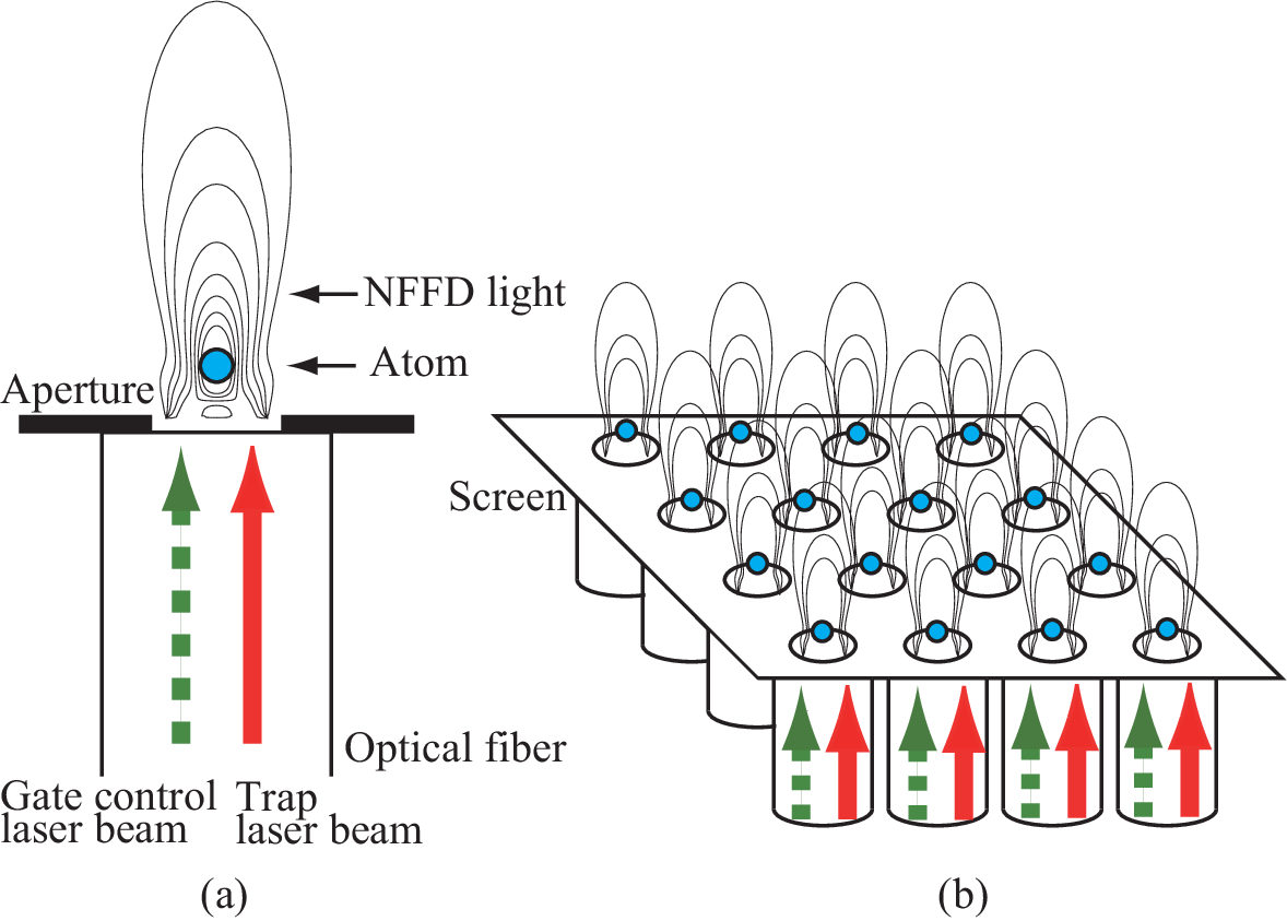
Figure 2 shows an array of optical traps, arranged in a regular 2-d lattice. It is clear by construction that we have freedom in the choice of the lattice constant and the lattice shape. We may even arrange the traps in an irregular form if necessary. This is a remarkable new feature, which a conventional optical lattice cannot provide with. An optical lattice is always regular, whose lattice constant is on the order of the wavelength of the laser beams.
Attached to each atom is an optical fiber, though which two laser beams are fed, one is for atom trapping while the other is to control the hyperfine qubit states of the atom. It is required to turn on and off the trap laser individually, which is required to implement a selective two-qubit gate as will be shown later. The gate control laser is also controllable so that one-qubit gates may be applied on many qubits simultaneously and independently.
IV Quantum Gate Implementations
For a quantum system to be a candidate of a general purpose quantum computer, it is necessary for the system to be able to implement a universal set of quantum gates, that is, the set of one qubit gates and almost any two-qubit gate [10]. Now we explain how these gates are realized in our proposal.
IV.1 One-Qubit Gates
Let us assume, for definiteness, the trap potential is strong enough so that inter-atomic interaction is switched off. Along with the NFFD trap light, there is a gate control laser beam propagating through the fiber, which is depicted in a green broken line in Fig. 2.
One-qubit gate is implemented by making use of the two-photon Raman transition [2]. Let and be the energy eigenvalues of the states and , respectively, and let be the energy eigenvalue of an auxiliary excited state necessary for the Raman transition. Suppose a laser beam with the frequency has been applied to the atom. Let be the detuning and be the Rabi oscillation frequency between the state and . Then, under the assumptions , we obtain the effective Hamiltonian
| (10) |
where
Note that generates all the elements of SU(2) since there are two generators in the Hamiltonian and their coefficients are controllable.
One-qubit gate implementations with the two-photon Raman transitions have been already demonstrated [8].
IV.2 Two-Qubit Gates
Although a two-qubit gate operation has been already experimentally demonstrated [6], a selective gate operation is yet to be realized. We propose to use a one-dimensional optical lattice or a set of optical lattices to selectively apply a two-qubit gate in the aforementioned setting. A one-dimensional optical lattice is made of a pair of counterpropagating laser beams with the same linear polarization, in which the basis states and are subject to the same trap potential. Alternatively, hyperfine-state-senstive trap potentials may be introduced if two counterpropagating laser beams with tilted polarizations, and , are superposed. This results in
| (11) |
where denote two circular polarizations. The electric field results in the Stark shifts
| (12) |
and detailed analysis of optical transitions shows that the effective potentials acting on and are
| (13) |
respectively, where use has been made of the following decompositions
| (14) |
It is important to note that () moves right (left) if is increased, which implies that the components and move in opposite directions as is changed.
Suppose a one-dimensional optical lattice, with the potential depth considerably shallower than that of the individual trap potential, is always superposed with the trap potentials. It is assumed that the lattice constant of the trap potential array is an integral multiple of the optical lattice period and the bottom of the trap potential sits in one of the bottoms of the optical lattice. The atom is in the motional ground state of the combined potential in an idle time.
Two qubit-gate operation is implemented with six steps. To simplify our exposition, we assume the trap array is a square lattice and two atoms, on which the gate acts, are aligned along one of the primitive lattice vectors. More general cases will be treated later.

- STEP 1
The Hadamard gate acts on each of the two qubits taking part in the gate operation by manipulating the control laser beams, which results in the superpostion of ,
- STEP 2
The trap potentials of the two qubits are turned off adiabatically so that the resulting motional states remain in the local ground states in the optical lattice.
- STEP 3
Then the trap potential array is shifted away from the optical lattice. The motional state of a qubit, which does not take part in the gate operation, ends up with the ground state of the shifted trap potential provided that the shift is adiabatically done. Now only the two qubits to be operated by the gate remain in the optical lattice.
- STEP 4
Polarizations of the counterpropagating laser beams are controlled so that of one qubit collides with of the other qubit. Then the vector obtains an extra dynamical phase factor , where is the energy shift due to the collision while is the time during which the two states are in contact [6].
- STEP 5
The components are put back to their initial positions in the optical lattice by reversing the change in .
- STEP 6
Then the screen is put back to its initial position so that the trap potentials overlap again with the optical lattice. Subsequently, the trap potentials of the two qubits, which were temporarily switched off, are turned on again. One-qubit gates may be applied on the two qubits if necessary.
In case the two atoms are in a general position, not necessarily along a primitive lattice vector, we may introduce two orthogonal optical lattices as shown in Fig. 4. Then the selected atomic states of one atom and of the other meet at the intersection of the two optical lattices to acquire the extra dynamical phase. It should be noted that two-qubit gate operations may be applied simultaneously and independently on many pairs of qubits.

Figure 4 (b) employs a radial array of NFFD traps. The radial center is the position where interaction of qubit states takes place. In the radial construction, however, simultaneous application of two-qubit gates on many pairs of qubits is difficult.
V Variations
There are several variations of the current proposal. Instead of leaving two atoms in the optical lattice and withdraw the rest of the atoms, we may initialize the register so that no atoms are present in the optical lattice. Then a pair of atoms are sent to the optical lattice by enlarging the size of the aperture as shown in Fig. 5, in which we indicate a double-layer construction. We may double the number of qubits and, at the same time, reduce the execution time with this implementation. Note that the vertical position of the atom is controllable by changing the aperture radius as was demonstrated in Fig. 1. Then we repeat the two-qubit gate operation (STEPs 4 and 5) outlined in the previous section to selectively entangle the pair of atoms.

The size of the aperture can be controlled by employing the well-established MEMS (MicroElectroMechanical Systems) technology. For example, an MEMS shutter for a display is already in a mass production stage [11] and it may be employed for physical realization of our proposal. We note that the on (off) time of the shutter is 54 (36) s [11] and we expect faster switching time by optimizing its structure for our purpose. [12]
Figure 6 shows the second variation, which involves many red-detuned laser beams and pairs of optical tweezers. Atoms are trapped at the intersections of mutually orthogonal red-detuned laser beams. Each vertical laser beam has another laser for two-photon Raman transition control employed for one-qubit gate operations. Horizontal laser beams are introduced for vertical confinement. A pair of optical tweezers implements two-qubit gates. The optical tweezer 1 is -polarized to produce a trap potential for a component , while the other (the optical tweezer 2) is -polarized to produce , which traps . These optical tweezers are manipulated to pick up the components from one atom and from the other. These states are put together for a duration as before to introduce a phase in the subspace . These components are put back to their initial positions after the contact.

Similar idea has been proposed in [13, 14], in which group-II-like atoms (such as Sr and Yb) are picked up by a pair of optical tweezers and, subsequently, they are made to collide with each other. Entanglement is established by taking advantage of the difference in the -wave scattering lengths (i.e., interaction strengths) of different electronic states of the atom.
Needless to say, we may mix these methods for the best implementation, which is compatible with the current technology.
VI Summary and Discussions
We proposed scalable designs of a neutral atom quantum computer with an on-demand interaction. A qubit is made of two hyperfine states of an atom. Associated with each atom, there is an optical fiber, through which a trap laser and a gate control laser are supplied. The latter is used to implement one-qubit gates by two-photon Raman transitions. One-qubit gate operations are applicable to all the qubits simultaneously and independently. A two-qubit gate may be implemented by leaving two qubit states, from one atom and from the other, in an optical lattice. By controlling the polarizations of counterpropergating laser beams, with which the optical lattice is formed, it is possible to collide these qubit states and introduce an extra dynamical phase in this particular two-qubit state . Two-qubit gate operations are also applicable on many pairs of qubits simultaneously and independently.
We believe our proposal is feasible within the existing technology. Now we are conducting extensive numerical analysis for each step and the results will be published elsewhere.
Acknowledgements.
We would like to thank Toshiki Ide for discussion in the early stage of this work. MN would like to thank Barry Sanders for drawing his attention to [13] and [14]. MN and TO are partly supported by Grant-in-Aid for Scientific Research (C) (Grant No. 19540422) from JSPS. A part of this research is also supported by “Open Research Center” Project for Private Universities: Matching fund subsidy from MEXT (Ministry of Education, Culture, Sports, Science and Technology).References
- [1] Quantum Information Science and Technology Roadmapping project; http://qist.lanl.gov/
- [2] M. Nakahara and T. Ohmi, Quantum Computing: From Linear Algebra to Physical Realizations (Taylor & Francis, 2008).
- [3] T. Yasuda, M. Tada-Umezaki, M. Nakahara, and T. Wakabayashi, arXiv:1004.0910v1 [quant-ph].
- [4] W. Harneit, Phys. Rev. A, 65, 032322 (2002). S. C. Benjamin et al., J. Phys.: Condens. Matter, 18 S867 (2006).
- [5] L. M. K. Vandersypen et el., Nature, 414, 883 (2001).
- [6] O. Mandel et al,, Nature, 425, 937 (2003).
- [7] O. Mandel et al., Phys. Rev. Lett. 91, 010407 (2003).
- [8] D. D. Yavuz et al., Phys. Rev. Lett. 96, 063001 (2006).
- [9] T. N. Bandi, V. G. Minogin, and S. N. Chormaic, Phys. Rev. A, 78, 013410 (2008).
- [10] A. Barenco et al., Phys. Rev. A 52, 3457 (1995).
- [11] http://www.pixtronix.com/
- [12]
http://www2.electronicproducts.com/MEMS_shutter_
array_to_revolutionize_optoelectronics-article-SEPOL1-sep2003-html.aspx - [13] R. Stock et al., Phys. Rev. A 78, 022301 (2008)
- [14] N. B. Babcock, et al., Can. J. Phys. 86, 549 (2008).