Electronic Structure Calculations with the Tran-Blaha Modified Becke-Johnson Density Functional
Abstract
We report a series of calculations testing the predictions of the Tran-Blaha functional for the electronic structure and magnetic properties of condensed systems. We find a general improvement in the properties of semiconducting and insulating systems, relative to calculations with standard generalized gradient approximations, although this is not always by the same mechanism as other approaches such as the quasiparticle GW method. In ZnO the valence bands are narrowed and the band gap is increased to a value in much better agreement with experiment. The Zn states do not move to higher binding energy as they do in LDA+U calculations. The functional is effective for systems with hydride anions, where correcting self-interaction errors in the 1 state is important. Similarly, it correctly opens semiconducting gaps in the alkaline earth hexaborides. It correctly stabilizes an antiferromagnetic insulating ground state for the undoped cuprate parent CaCuO2, but seriously degrades the agreement with experiment for ferromagnetic Gd relative to the standard local spin density approximation and generalized gradient approximations. This is due to positioning of the minority spin states at too low an energy. Conversly, the position of the La conduction bands of La2O3 is in reasonable accord with experiment as it is with standard functionals. The functional narrows the Fe bands of the parent compound LaFeAsO of the iron high temperature superconductors, while maintaining the high Fe spectral weight near the Fermi energy.
I introduction
Density functional theory (DFT) is formally a theory for the ground state and not for the spectroscopic properties, at least not with the interpretation of Kohn-Sham eigenvalues as a one electron spectrum. In fact, DFT based methods, using modern generalized gradient approximations [1, 2] (GGA)s give extremely useful total energies and structural properties for a wide range of materials, but is known to strongly underestimate band gaps in most semiconductors and insulators. It also suffers from incorrect predictions of metallic or very small band gap semiconducting states in Mott insulators, and in the case of undoped cuprates (e.g. La2CuO4 and CaCuO2) produces an incorrect non-magnetic ground state in contrast to the actual antiferromagnetic insulating state.
An important aspect of standard DFT calculations is that they are computationally efficient. This allows detailed calculations for wide variety of complex materials including their full realistic chemical and structural details. This greatly facilitates comparison with experiment. Similarly and in spite of the known problems with standard DFT calculations, such calculations have proved to be very useful in understanding electronic spectra of solids, both through interpretation of experiments and predictions. Methods that retain the computational efficiency of standard DFT, but improve the spectroscopic properties are potentially of great interest. In this regard, Tran and Blaha have recently developed a semi-local functional [3] based on a modification of the Becke-Johnson functional. [4] Importantly, this is not a hybrid functional, and therefore scales like standard DFT rather than Hartree-Fock in solids. They showed that this functional gives very much improved band gaps for a variety of insulators, including semiconductors, oxides, rare gas solids and lithium halides. [3] They also found substantial gaps in accord with experiment for the 3 transition metal monoxides, MnO, FeO and especially the prototypical Mott insulator NiO. Calculations of the optical properties for a variety of heavier halides also showed much improved agreement with available experimental data. [5]
Here we present further tests of this functional emphasizing systems that are difficult to describe for a variety of different reasons. We also discuss in more detail the electronic structure of ZnO, which was one of the systems studied by Tran and Blaha. We find general improvements in the band gaps over the standard PBE functional in all materials. We also find an antiferromagnetic insulating ground state for the Mott insulator CaCuO2. However, the electronic structure differs from that predicted by other methods and its consistency with experimental data as regards the distribution of the spectral weight is not clear. The electronic structure of ferromagnetic Gd is degraded with respect to the standard PBE functional.
II approach
The calculations were performed with the standard general potential linearized augmented planewave (LAPW) method with local orbitals, [6, 7] as implemented in the WIEN2k package. [8] We use the Perdew Burke Ernzerhof (PBE) GGA as a reference, with the exception of CaCuO2, where we use PBE+U calculations, with Coulomb parameter -=7 eV and self-interaction correction [9] (SIC) and about mean field [10] (AMF) double counting corrections, since standard GGAs do not produce an antiferromagnetic ground state in that case. [11] Except as noted, we used experimental lattice parameters and relaxed all non-symmetry fixed internal coordinates with the PBE GGA. Also, except as noted, we performed calculations in a scalar relativistic approximation for the valence states, while core states were treated relativistically. The basis sets and zone samplings were well converged, with additional local orbitals used to relax linearization errors. We used the standard LAPW matching as opposed to the faster augmented planewave plus local orbital (APW+lo) approach. [12]
III semiconductors and non-magnetic insulators
We begin with ZnO, which is a well studied material with a band gap of 3.44 eV. Standard functionals give an unusually large band gap error in this material. Correcting this error is of considerable importance in understanding the defect physics and semiconducting properties of ZnO. [13] Our PBE calculations, which we performed with the experimental lattice parameters of =3.2489 Å, =5.2049 Å, and internal parameter =0.381 yield a band gap of 0.80 eV. The band structure is shown in Fig. 1. The unusually large underestimate is generally thought to be associated with a position of the Zn 3 bands at too low binding energy with respect to the valence band edge. [14, 15] In this case, the resulting overly large level repulsion between the states and valence bands pushes the valence band maximum up, reducing the band gap. This view is supported by photoemission measurements, which place the states 7 – 8 eV below the valence band edge, [16, 17] although it should be noted that this could possibly reflect properties of the surface and not the bulk. Considering the importance of this material it would be desirable to further check the position of the Zn bands, for example by higher energy photoemission or other spectroscopies.


The band gap error is largely corrected by GW calculations. [18, 15] These calculations place the Zn at high binding energy 6.5 eV, as compared to -5 eV in standard PBE calculations (see Fig. 2). The error in the band gap is also greatly improved in LDA+U calculations, where the Coulomb parameter is used to shift the Zn orbitals to higher binding energy. [14] Hybrid functional calculations also greatly improve the band gap and shift the states to higher binding energy. [19] We obtained a band gap of 2.65 eV, which is much improved relative to the PBE functional, but is still lower than experiment. This is almost exactly the same value as that reported by Tran and Blaha. [3] Our band structure (Figs. 1 and 2) shows Zn bands that are narrowed relative to the PBE result, but are not shifted to higher binding energy. This may well be the origin of the remaining discrepancy between the TB-mBJ and experimental band gaps.


We next discuss La2O3. This high-k dielectric oxide occurs in a hexagonal ( number 164) structure with lattice parameters =3.943 Å, and =6.141 Å. Our calculated internal coordinates are =0.2468 and =0.6458, in good agreement with the experimental values of 0.2467 and 0.6470, respectively. [20] La2O3 has a low temperature optical band gap of 5.34 eV. [21] The calculated PBE and TB-mBJ band structures and densities of states (DOS) are shown in Figs. 3 and 4, respectively. The valence bands are derived from O states. In the PBE calculation the conduction bands come from La states that hybridize with La states that occur just above the band edge, while in the TB-mBJ calculation the conduction bands come from the La states. Obtaining a correct band gap in this compound depends on a correct placement of the La resonance. The calculated TB-mBJ band gap is 4.74 eV, which is higher than the PBE value of 3.85 eV. It is in much better agreement with experiment but still 0.6 eV too low. Most likely this reflects the position of the La resonance. Interestingly, the position of the La resonance with respect to the O derived valence band edge is almost the same in the PBE and TB-mBJ calculations, although the bands are narrower with the latter functional because the other conduction bands are shifted to higher energy. This behavior is reminiscent of what we found for La halides. [5]
IV Ferromagnetic Gd


We next discuss an open shell material. Gd is a ferromagnetic metal, with a half filled shell. This leads to a high spin moment, nominally 7 from the electrons. The actual experimental moment per atom is 7.63 , which includes a contribution from polarization of the other valence states. [22, 23, 24] The value of the moment is not sensitive to the treatment of the electrons provided that they remain fully polarized, as they do in standard DFT and LDA+U calculations. [25, 26] On the other hand, standard DFT calculations produce a Fermi energy density of states, , that is higher than that inferred from specific heat measurements. While there can be an enhancement of the specific heat in experiments for a variety of reasons, such as electron-phonon interactions, spin fluctuations, etc., a reduction is difficult to understand. The high in calculations comes about because the minority spin states, while above the Fermi energy, are close to it, and hybridize with the valence bands. LDA+U calculations move the minority bands to higher energy, reducing the hybridization and improving agreement with experiment. In effect, standard DFT calculations underestimate the exchange splitting of the shell.
We performed calculations for hcp ferromagnetic Gd, including spin orbit with the experimental lattice parameters, [27] =3.629 Å, =5.796 Å. We aligned the magnetization with the -axis.
The band structures and DOS are shown in Figs. 5 and 6, respectively. As may be seen, the TB-mBJ functional keeps the average position approximately the same as in the PBE calculations, but reduces the exchange splitting opposite to LDA+U calculations. This brings additional character to the Fermi energy, reduces the moment, and increases . On a per atom basis we obtain =1.73 eV-1 with the PBE functional and 3.64 eV-1 with the TB-mBJ functional. The inferred experimental specific heat value is 1.57 eV-1. [28] Our calculated PBE spin moment is 7.62 in agreement with experiment and prior studies, while the TB-mBJ value is 6.65 . Therefore, it may be concluded that the TB-mBJ functional seriously degrades agreement with experiment for ferromagnetic Gd.
V hydrides
Hydrides present an interesting challenge to DFT calculations, particularly anionic hydrides. Standard DFT calculations have large errors in their descriptions of the one electron H atom because of an incomplete cancellation of the Hartree and exchange correlation self-interactions. The trihydride, YH3, which is a transparent insulator, is incorrectly described as a metal in the LDA. This has been attributed to self-interaction on the H, the ordinary problems in describing band gaps within the LDA, other correlation effects, and complications with the crystal structure. [29, 30, 31, 32, 33, 34, 35, 36, 37, 38] Several calculations have shown that a semiconducting gap can be opened in GW quasiparticle calculations and also the with the non-local weighted density approximation (WDA) to DFT. [36] The WDA is self-interaction free for one electron systems. Unfortunately, while the insulating behavior of YH3 is likely an electronic effect and not a consequence of structural details, [39] the fact that the exact structure is uncertain complicates interpretation of calculated results.
Here we present results for three well studied hydrides, specifically LiH, MgH2 and AlH3. LiH occurs in the fcc NaCl structure. Our calculations were done with the experimental lattice parameter for LiD at 83K, =4.0447 Å. [40] MgH2 is tetragonal, with a rutile structure. We used the experimental lattice parameters, =4.5198 Å, =3.025 Å. [41] The internal H coordinate, was kept at its experimental value of =0.30478 since the force on H was found to be small with this value. AlH3 occurs in a hexagonal, structure. [42] We used the experimental lattice parameters, =4.449 Å, =11.804 Å, and relaxed internal coordinate. The structure has Al on site 6 (0,0,0) and H on site 18 (,0,1/4), with =0.6319, in good accord with the reported experimental value of =0.628 (Ref. 42).
Our calculated PBE and TB-mBJ band structures are given in Figs. 7, 8 and 9, for LiH, MgH2 and AlH3, respectively. The corresponding DOS are in Figs. 10 and 11 for LiH and AlH3. Our PBE band structures are similar to those obtained in prior DFT calculations. [43, 44, 45, 46] The band gaps are of charge transfer character between predominantly H derived valence bands and predominantly metal derived conduction bands.
We start with LiH. Both functionals predict a direct gap at the point. The calculated band gaps are 3.01 eV and 5.08 eV for the PBE and TB-mBJ functionals, respectively. The experimental band gap of LiH is 5.0 eV as quoted in Ref. 44. Thus the TB-mBJ is in almost perfect agreement with experiment for LiH. MgH2 has an indirect gap. The PBE and TB-mBJ values are 3.70 eV and 5.74 eV, respectively. The experimental band gap of MgH2 is 5.6 eV. [47] Therefore, as in LiH, almost perfect agreement with experiment is obtained with the TB-mBJ functional. We are not aware of an experimental band gap for AlH3, but recent GW calculations yield a values of 3.54 eV or 4.31 eV depending on the treatment. [44] Our values are 2.27 eV and 4.31 eV for the PBE and TB-mBJ functionals. In the cases studied the valence bands are somewhat narrower with the TB-mBJ functional relative to the PBE results. The results for hydrides with the TB-mBJ functional are very encouraging.


VI CaB6 and SrB6
The hexaborides CaB6 and SrB6 are modest band gap semiconductors. [48, 49, 50, 51] Like the anionic hydrides they have charge transfer gaps between valence bands derived from a compact orbital where self-interactions may be important and conduction bands with metal atom character. In this case the valence bands are derived from B states. Also, similar to YH3, standard DFT calculation predict a semimetallic state due to a band overlap, while both WDA and GW calculations yield small insulating gaps. [52, 53, 54]
The nature of the bands is, however, different from the hydrides. In the hydrides the valence bands are nominally from the filled H state, while the conduction bands are nominally from the metal orbitals, although there may be some hybridization. In the hexaborides, the bonding of the B network plays a central role. The valence bands are derived from bonding combinations of B states, while the conduction bands come from mixtures of non-bonding and antibonding B states with Ca/Sr states. The center of the metal states is at 4 eV above the band gap, but the hybridization of B and Ca/Sr orbitals persists down to the conduction band minimum. The band gap underestimation could therefore come from incomplete cancellation of self-interaction errors in the B derived valence bands, or alternatively an overestimate of the B - Ca/Sr hybridization that then pushes the conduction band minimum down (analogous to the pushing up of the valence band edge in ZnO), or a combination of these two possible errors.
We did calculations for CaB6 and SrB6 using the experimental simple cubic crystal structures. We did not relax the internal B coordinate because the forces with the experimental values were small. The lattice parameters used were 4.1514 Å, for CaB6, and 4.1953 Å, for SrB6. The internal coordinates were =0.2019 for CaB6 and =0.2031 for SrB6. Our calculated band structures for CaB6 and SrB6 are given in Figs. 12 and 13, respectively. The corresponding DOS are in Figs. 14 and 15.
We find a metallic state in PBE calculations due to band overlap at the point in both materials. On the other hand, with the TB-mBJ functional we obtain small gaps: 0.10 eV for CaB6 and 0.18 eV for SrB6. There is a wide range in measured band gap values for the hexaborides. However, recent optical measurements for CaB6 yield a band gap of 0.25 eV, [51] while prior measurements indicate a larger gap 1 eV. [48, 49, 50] Considering the dependent resistivity, and the spectroscopic measurements, the TB-mBJ result is clearly better than that of the PBE calculation, but the gap is underestimated. In contrast to the hydrides, we do not find a valence band narrowing with the TB-mBJ functional. Also, the position of the Ca/Sr states in the DOS (not shown) at 4 eV is almost exactly the same in the PBE and TB-mBJ calculations. It will be desirable to check this against spectroscopic data, if such data becomes available. An upward shift of the bands would increase the band gap.


VII CaCuO2
As mentioned, Tran and Blaha reported calculations for the transition metal monoxides, MnO, FeO and NiO finding improved band gaps along with changes in the density of states of NiO that differ from those found in LDA+U calculations. [3] Here we present calculations for CaCuO2. This material is the simplest parent compound representative of undoped cuprate superconductors.
These materials are Mott insulators when undoped, and become high temperature superconductors when doped. Importantly, they have a non-trivial band structure associated with strong hybridization between Cu orbitals, particularly the bonding Cu - O combinations. These combinations lead to an antibonding band, of orbital symmetry crossing the Fermi energy and giving rise to the Fermi surface on which superconductivity occurs. This hybridization also leads to a large interatomic exchange coupling, and high magnetic energy scale, which may be important for the high superconducting critical temperatures. When undoped, this band is half filled, and as mentioned the Fermi surface is destroyed in favor of a Mott insulator. While the Fermi surfaces of the doped phases are generally well described in DFT calculations, the magnetism in these materials is not. [11, 55] In contrast to MnO, FeO and NiO, these materials are described as non-magnetic in DFT calculations, and so the ground state is qualitatively wrong, not only in terms of electronic structure but also in the fact that there is no moment formation. This can be corrected by LDA+U (or GGA+U) methods, which yield an insulating antiferromagnetic ground state. [56] These methods also shift the spectral weight away from the Fermi energy to form what may be termed upper and lower Hubbard bands. This shift of spectral weight away from the Fermi energy is consistent with photoemission measurements. [57] However, while there is a shift towards Hubbard bands at high binding energy in both doped and undoped cuprates, there does remain spectral weight at the band edge in the insulators and Fermi energy in the superconductors.
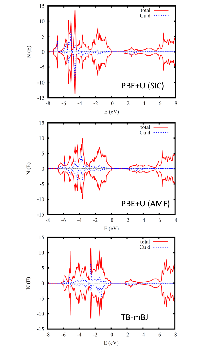
We performed calculations using the PBE+U method, with -=7 eV and two double counting corrections, the self-interaction correction (SIC) scheme and the about mean field (AMF) scheme. We used the experimental tetragonal crystal structure (there are no internal coordinates). [58] For the magnetic order we assumed a G-type ground state, i.e. the in-plane nearest neighbor checkerboard antiferromagnetism that is common to cuprates with antiferromagnetic stacking along the -axis.
The resulting electronic DOS are compared with results obtained using the TB-mBJ functional (and no added ) in Fig. 16. First of all we note that unlike standard DFT treatments the TB-mBJ functional successfully stabilizes the antiferromagnetic insulating state. The calculated spin moments as measured by the polarization inside the Cu LAPW sphere (radius 2.0 Bohr) are 0.636 , 0.695 , and 0.646 for the PBE+U (SIC), PBE+U (AMF) and TB-mBJ functionals, respectively. The reduction from the ideal spin 1/2 value of 1 reflects hybridization with the O states. The calculated band gaps are sensitive to the value of - assumed in the PBE+U calculations. With the value of 7 eV used here, we obtained gaps of 1.5 eV and 1.3 eV with the SIC and AMF double counting schemes, respectively. The TB-mBJ gap is comparable at 1.7 eV. The essential difference between the PBE+U and TB-mBJ results is seen in the distribution of the Cu DOS. The two double counting schemes, yield somewhat different distributions of the DOS, but both have a strong shift of the occupied DOS to higher binding energy. The TB-mBJ DOS instead places substantial DOS near the valence band edge. This is similar to what Tran and Blaha found in NiO. In cuprates, it is clear that there are Hubbard bands at high binding energy, which are present in the PBE+U but not the TB-mBJ calculations. However, it is unclear from existing experimental data whether the description near the valence band edge is better with the PBE+U or the TB-mBJ functionals. One possible avenue for resolving this is to note that when projected onto a given site, the Cu character near the band edge with the TB-mBJ functional has a substantial spin polarization, which could in principle be detected in spin polarized scanning probe experiments.
VIII LaFeAsO


The iron based superconductors provide an interesting contrast to the cuprates. [59] Unlike cuprates, these materials show strong spectral weight around the Fermi energy, in accord with DFT calculations, weak to moderate correlations, and no Hubbard bands. [60] DFT calculations, [61] show an Fe metal, with a high density of states and a semimetallic character, i.e. small Fermi surfaces: hole-like sheets around the zone center, and two electron sheets at the zone corner. These features are in accord with experiment, and are degraded by methods that build in strong correlations. One difference between DFT calculations and experiment is that the bands are narrower in experiment. [60, 62]
We performed calculations for LaFeAsO using the experimental 175 K crystal structure of de la Cruz and co-workers, [63] including the experimental internal coordinates. We did not relax the internal coordinates because they are known to be incorrectly given by non-magnetic GGA calculations, while magnetic calculations incorporating the spin density wave give overly strong magnetism, presumably due to spin fluctuations neglected in DFT calculations. [64, 65] In any case, this should be kept in mind when comparing calculations, since the band structure, especially near the zone center, is sensitive to the As position in the unit cell. In particular, there are additional hole sheets of Fermi surface that depend on whether one uses the experimental or calculated As position. Here we focus on the large scale features of the electronic structure that are not dependent on this choice. These are the energy dependent character of the bands and the shape of the main Fermi surface, which governs superconductivity. [66]
The calculated non-spin-polarized DOS, band structure and Fermi surfaces are shown in Figs. 17, 18 and 19, respectively. As may be seen, the bands within 2 eV of are of mainly Fe character with modest hybridization of As states in both the PBE and TB-mBJ calculations. The As and O bands are at higher binding energy, yielding nominally Fe2+ metallic sheets. Also in both calculations there is a pseudogap in the DOS starting near corresponding to the semimetallic character. This is seen in the small disconnected Fermi surfaces. One difference is that the TB-mBJ calculation has a 10% smaller band width, which would marginally improve agreement with experiment. The detailed dispersions of the bands near are different between the two calculations. The electron pockets are larger in the TB-mBJ calculation. Also, there is one fewer small hole Fermi surface section. However, while these features may be important to understanding the materials, they are at the level of differences that arise from different treatments of the As position, and we do emphasize them here. The overall agreement of the PBE and TB-mBJ results in this material is gratifying.
IX summary and conclusions
We performed calculations for a diverse set of materials using the recently developed semilocal density functional of Tran and Blaha. The present results taken in combination with the tests that they reported [3] and calculations for halides [5] strongly support the conclusion that this functional greatly improves the band gaps and electronic structure of simple semiconductors and insulators. It also greatly improves upon standard density functionals in that it stabilizes an antiferromagnetic insulating ground state in CaCuO2. However, the quality of the description of bands still needs clarification. In ZnO, the Zn states may be too shallow, and in CaCuO2 the distribution the DOS in the valence bands differs from that obtained with the standard LDA+U method. The large scale features of the TB-mBJ electronic structure of LaFeAsO are similar to those with the PBE functional, although there are changes in details that affect the hole Fermi surface sections. Turning to band materials, the properties of La2O3 are improved relative to PBE calculations, although the bands are hardly affected at all by the change in functional. On the other hand, the properties of ferromagnetic Gd are seriously degraded with respect to the PBE functional.
In summary, the results indicate that the TB-mBJ functional is a very useful development for treating the electronic structure of simple semiconductors and insulators, including hydrides, while care is needed in applying it to and band materials.
Acknowledgements.
Work at ORNL was supported by the Department of Energy, ORNL LDRD Program (insulators) and the Office of Basic Energy Sciences, Materials Sciences and Engineering Division (metals).References
- [1] J. P. Perdew, J. A. Chevary, S. H. Vosko, K. A. Jackson, M. R. Pederson, D. J. Singh, and C. Fiolhais, Phys. Rev. B 46, 6671 (1992)
- [2] J. P. Perdew, K. Burke, and M. Ernzerhof, Phys. Rev. Lett. 77, 3865 (1996)
- [3] F. Tran and P. Blaha, Phys. Rev. Lett. 102, 226401 (2009)
- [4] A. D. Becke and E. R. Johnson, J. Chem. Phys. 124, 221101 (2006)
- [5] D. J. Singh, arXiv:1008.2175(2010)
- [6] D. J. Singh and L. Nordstrom, Planewaves, Pseudopotentials and the LAPW Method, 2nd Ed. (Springer Verlag, Berlin, 2006)
- [7] D. Singh, Phys. Rev. B 43, 6388 (1991)
- [8] P. Blaha, K. Schwarz, G. Madsen, D. Kvasnicka, and J. Luitz, WIEN2k, An Augmented Plane Wave + Local Orbitals Program for Calculating Crystal Properties (K. Schwarz, Tech. Univ. Wien, Austria)(2001)
- [9] V. I. Anisimov, I. V. Solovyev, M. A. Korotin, M. T. Czyzyk, and G. A. Sawatzky, Phys. Rev. B 48, 16929 (1993)
- [10] M. T. Czyzyk and G. A. Sawatzky, Phys. Rev. B 49, 14211 (1994)
- [11] D. J. Singh and W. E. Pickett, Phys. Rev. B 44, 7715 (1991)
- [12] E. Sjostedt, L. Nordstrom, and D. J. Singh, Solid State Commun. 114, 15 (2000)
- [13] S. Lany and A. Zunger, Phys. Rev. B 78, 235104 (2008)
- [14] R. Laskowski and N. E. Christensen, Phys. Rev. B 73, 045201 (2006)
- [15] M. Shishkin, M. Marsman, and G. Kresse, Phys. Rev. Lett. 99, 246403 (2007)
- [16] R. A. Powell, W. E. Spicer, and J. C. McMenamin, Phys. Rev. Lett. 27, 97 (1971)
- [17] K. Ozawa, K. Sawada, Y. Shirotori, and K. Edamoto, J. Phys. Condens. Matter 17, 1271 (2005)
- [18] M. van Schilfgaarde, T. Kotani, and S. V. Faleev, Phys. Rev. B 74, 245125 (2006)
- [19] J. Uddin and G. E. Scuseria, Phys. Rev. B 74, 245115 (2006)
- [20] Y. E. Bogatov, O. A. Ochieng, A. K. Molodkin, and M. G. Safronenko, Zh. Neorg. Khim. 41, 856 (1996)
- [21] S. I. Kimura, F. Arai, and M. Ikezawa, J. Phys. Soc. Jpn. 69, 3451 (2000)
- [22] L. W. Roeland, G. J. Cock, F. A. Muller, A. C. Moleman, K. A. McEwen, R. G. Jordan, and D. W. Jones, J. Phys. F 5, L233 (1975)
- [23] G. Schutz, M. Knulle, R. Wienke, W. Wilhelm, W. Wagner, P. Kienle, and R. Frahm, Z. Phys. B 73, 67 (1988)
- [24] P. A. Dowben, D. LaGraffe, and M. Onellion, J. Phys. Condens. Matter 1, 6571 (1989)
- [25] D. J. Singh, Phys. Rev. B 44, 7451 (1991)
- [26] S. Abdelouahed, N. Baadji, and M. Alouani, Phys. Rev. B 75, 094428 (2007)
- [27] J. R. Banister, S. Legvold, and F. H. Spedding, Phys. Rev. 94, 1140 (1954)
- [28] P. Wells, P. C. Lanchester, D. W. Jones, and R. G. Jordan, J. Phys. F 4, 1729 (1974)
- [29] J. A. Alford, M. Y. Chou, E. K. Chang, and S. G. Louie, Phys. Rev. B 67, 125110 (2003)
- [30] K. K. Ng, F. C. Zhang, V. I. Anisimov, and T. M. Rice, Phys. Rev. Lett. 78, 1311 (1997)
- [31] K. K. Ng, F. C. Zhang, V. I. Anisimov, and T. M. Rice, Phys. Rev. B 59, 5398 (1999)
- [32] P. van Gelderen, P. A. Bobbert, P. J. Kelly, and G. Brocks, Phys. Rev. Lett. 85, 2989 (2000)
- [33] R. Eder, H. F. Pen, and G. A. Sawatzky, Phys. Rev. B 56, 10115 (1997)
- [34] P. van Gelderen, P. J. Kelly, and G. Brocks, Phys. Rev. B 63, 100301 (2001)
- [35] T. Miyake, F. Aryasetiawan, H. Kino, and K. Terakura, Phys. Rev. B 61, 16491 (2000)
- [36] Z. Wu, R. E. Cohen, D. J. Singh, R. Gupta, and M. Gupta, Phys. Rev. B 69, 085104 (2004)
- [37] P. J. Kelly, J. P. Dekker, and R. Stumpf, Phys. Rev. Lett. 78, 1315 (1997)
- [38] R. Ahuja, B. Johansson, J. M. Wills, and O. Eriksson, Appl. Phys. Lett. 71, 3498 (1997)
- [39] A. T. M. van Gogh, E. S. Kooij, and R. Griessen, Phys. Rev. Lett. 83, 4614 (1999)
- [40] G. Vidal-Valat, J. P. Vidal, K. Kurki-Suonio, and R. Kurki-Suonio, Acta Cryst. A 48, 46 (1992)
- [41] S. Ono, Y. Ishido, K. Imanari, T. Tabata, Y. K. Cho, R. Yamamoto, and M. Doyama, J. Less Com. Met. 88, 57 (1982)
- [42] J. W. Turley and H. W. Rinn, Inorg. Chem. 8, 18 (1969)
- [43] C. Moyses Araujo, S. Lebeque, O. Eriksson, B. Arnaud, M. Alouani, and R. Ahuja, J. Appl. Phys. 98, 096106 (2005)
- [44] M. J. van Setten, V. A. Popa, G. A. de Wijs, and G. Brocks, Phys. Rev. B 75, 035204 (2007)
- [45] S. Lebegue, M. Alouani, B. Arnaud, and W. E. Pickett, Europhys. Lett. 63, 562 (2003)
- [46] S. Z. Karazhanov, A. G. Ulyashin, P. Ravindran, and P. Vajeeston, EPL 82, 17006 (2008)
- [47] J. Isidorsson, I. A. M. E. Giebels, H. Arwin, and R. Griessen, Phys. Rev. B 68, 115112 (2003)
- [48] S. Souma, H. Komatsu, T. Takahashi, R. Kaji, T. Sasaki, Y. Yokoo, and J. Akimitsu, Phys. Rev. Lett. 90, 027202 (2003)
- [49] J. D. Denlinger, J. A. Clack, J. W. Allen, G. H. Gweon, D. M. Poirier, C. G. Olson, J. L. Sarrao, A. D. Bianchi, and Z. Fisk, Phys. Rev. Lett. 89, 157601 (2002)
- [50] B. K. Cho, J. S. Rhyee, B. H. Oh, M. H. Jung, H. C. Kim, Y. K. Yoon, J. H. Kim, and T. Ekino, Phys. Rev. B 69, 113202 (2004)
- [51] J. H. Kim, Y. Lee, C. C. Homes, J. S. Rhyee, B. K. Cho, S. J. Oh, and E. J. Choi, Phys. Rev. B 71, 075105 (2005)
- [52] H. J. Tromp, P. van Gelderen, P. J. Kelly, G. Brocks, and P. A. Bobbert, Phys. Rev. Lett. 87, 016401 (2001)
- [53] H. Kino, F. Aryasetiawan, K. Terakura, and T. Miyake, Phys. Rev. B 66, 121103(R) (2002)
- [54] Z. Wu, D. J. Singh, and R. E. Cohen, Phys. Rev. B 69, 193105 (2004)
- [55] W. E. Pickett, H. Krakauer, R. E. Cohen, and D. J. Singh, Science 255, 46 (1992)
- [56] V. I. Anisimov, J. Zaanen, and O. K. Andersen, Phys. Rev. B 44, 943 (1991)
- [57] A. Damascelli, Z. Hussain, and Z. X. Shen, Rev. Mod. Phys. 75, 473 (2003)
- [58] J. Karpinski, H. Schwer, I. Mangelschots, K. Conder, A. Morawski, T. Lada, and A. Pasezewin, Physica C 234, 10 (1994)
- [59] Y. Kamihara, T. Watanabe, M. Hirano, and H. Hosono, J. Am. Chem. Soc. 130, 3296 (2008)
- [60] D. H. Lu, M. Yi, S. K. Mo, A. S. Erickson, J. Analytis, J. C. Chu, D. J. Singh, Z. Hussain, T. H. Geballe, I. R. Fisher, and Z. X. Shen, Nature (London) 455, 81 (2008)
- [61] D. J. Singh and M. H. Du, Phys. Rev. Lett. 100, 237003 (2008)
- [62] M. M. Qazilbash, J. J. Hamlin, R. E. Baumbach, L. Zhang, D. J. Singh, M. B. Maple, and D. N. Basov, Nature Physics 5, 647 (2009)
- [63] C. de la Cruz, Q. Huang, J. W. Lynn, J. Y. Li, W. Ratcliff II, J. L. Zaretsky, H. A. Mook, G. F. Chen, J. L. Luo, N. L. Wang, and P. C. Dai, Nature (London) 453, 899 (2008)
- [64] I. I. Mazin, M. D. Johannes, L. Boeri, K. Koepernik, and D. J. Singh, Phys. Rev. B 78, 085104 (2008)
- [65] D. J. Singh, Physica C 469, 418 (2009)
- [66] I. I. Mazin, D. J. Singh, M. D. Johannes, and M. H. Du, Phys. Rev. Lett. 101, 057003 (2008)