Charge transfer between epitaxial graphene and silicon carbide
Abstract
We analyse doping of graphene grown on SiC in two models which differ by the source of charge transfered to graphene, namely, from SiC surface and from bulk donors. For each of the two models, we find the maximum electron density induced in monolayer and bilayer graphene, which is determined by the difference between the work function for electrons in pristine graphene and donor states on/in SiC, and analyse the responsivity of graphene to the density variation by means of electrostatic gates.
Graphene [1] - monolayer or bilayer of carbon atoms with a honeycomb lattice - is a gapless semiconductor, which can be used as a current-carrying element in field-effect transistors. It has been found that the epitaxial graphene grown onto cm-size wafers of the Si-terminated face of SiC [2, 3, 4] maintains structural integrity over large area and demonstrates a relatively high mobility of carriers [5, 6, 7]. This makes graphene synthesized on SiC (SiC/G) a promising platform to build integrated electronic circuits, assuming one can control the carrier density in it. For transistor applications, bilayer graphene in SiC/G is a particularly interesting material, since interlayer asymmetry (e.g., induced by a transverse electric field) opens a minigap in its spectrum [8, 9].
In this Letter we present a theory of charge transfer from SiC to the epitaxial monolayer (MLG) and bilayer (BLG) graphene grown on its surface. It has been noticed that epitaxial graphene is always substantially n-doped, so that use of SiC/G in transistors requires reduction of carrier density using gates [4]. The initial doping of graphene comes from a combination of bulk donors in SiC with the volume density and surface donor states with the sheet density of surface states, (DoS). The charge transfer to graphene in a top-gated field-effect transistor can be found from solving two coupled equations:
| (1) | |||
| (2) |
Equation (1) accounts for the charge balance, with () being the areal density of electrons transferred to the gate. Here, / is the difference between the work function of graphene and the work function of electrons in the bulk/surface donors in SiC, and is the Fermi energy in doped graphene. Equation (2) describes the equilibrium between electrons in graphene and bulk donors, with standing for the depletion layer width in SiC, being the height of the Shottky barrier ( is dielectric constant of SiC), and - the distance between the SiC surface and the middle of graphene layer.
In the following, we calculate the density of electrons (for both MLG and BLG) in two limits: graphene doping dominated by the charge transfer from (a) surface donors, which corresponds to solving Eq. (1) with , and (b) bulk donors (e.g. nitrogen), which corresponds to solving Eqs. (1,2) with . Charge transfer in a more generic situation, with arbitrary and , can be assessed by taking the largest of the two estimates. Then, we determine the responsivity factor, , which characterizes the ability to control the carrier density using external gates: would be optimal for transistor operation of gated SiC/G devices whereas would indicate that transistor operation is impossible.
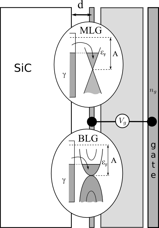
Monolayer graphene (MLG) has linear spectrum , in the two valleys, corresponding to the non-equivalent corners and of the hexagonal Brillouin zone, so that (we take into account both valley and spin degeneracy of the electron states). In the limit (a) we find that the carrier density is
| (3) |
The initial density of electrons in graphene is described by Eq. (3) () with two characteristic regimes,
| (4) |
where and are, respectively, the saturation value for the carrier density in SiC/G and the crossover value of DoS of donors on the SiC surface at which saturates:
| (5) |
The responsivity of MLG in SiC/G is, then,
| (6) |
In the limit (b) we find by solving Eqs. (1,2) numerically. The numerical solution shown in Fig. 2 (d) interpolates between the regimes of weak and strong graphene doping:
The responsivity, of MLG in SiC/G in the limit (b) can be described using Eq. (6), but with replaced by and the upper/lower limits corresponding to and , respectively.

Bilayer graphene (BLG) has the spectrum [8] with conduction (+) and valence (-) bands, which, in the vicinity of the Brillouin zone corners, are described by
where, is the interlayer coupling and distinguishes between pairs of degenerate () and split () bands. The Fermi level in n-doped BLG with sheet electron density is determined as
where cm-2.
In the limit (a), this gives
for and . Here, and . For larger densities, ,
which resembles Eq. (3) for MLG, but with .
Similarly to MLG, the density in BLG on SiC saturates upon the increase of surface DoS of donors. The crossover to the saturated density, , occurs at
The dependence of , and on the relative size of the band splitting , and the graphene-surface donors work function is shown in Fig. 2 (a-c). Responsivity of the BLG to the gate voltage is high or low, depending on whether the saturation regime for the carrier density is reached, or not. For , . For ,
| (9) |
In the limit (b), when is determined by charge transfer from bulk donors in SiC,
with , and responsivity of BLG requires that , whereas for responsivity is described by the same limits as in Eq. (9), with replaced by .
Independently of the number of layers, the gate voltage needed to reach the neutrality point in graphene controlled by the top gate with mutial capacitance is
| (10) |
In summary, we calculated charge transfer from SiC to epitaxial graphene. In the case when the charge transfer is dominated by donors on the surface of SiC with eV or donors in the bulk of SiC with eV, [12], we estimate that the saturation density of n-type doping of MLG is cm-2, which corresponds to eV (for nm). This value of carrier density occurs when the donor volume density is cm-3 (we use for 6H SiC [13]) or the surface states have DoS cm-2eV-1. For lesser doping of SiC, and , one should use the larger of the estimates from Eqs. (4,Charge transfer between epitaxial graphene and silicon carbide) This can be compared to the data reported in the recent studies of epitaxial graphene indicating a substantial initial level of n-type doping of SiC/G, very often [4] as high as 1013cm-2. However, some particular growth processes produce SiC/G with a much lower doping level [11, 5], indicating that efficient annealing of donors on and near the SiC surface is possible.
We thank T. Seyller and R. Yakimova for discussions. This work was supported by EPSRC grant EP/G041954 and EU-FP7 ICT STREP Concept Graphene.
References
- [1] A. K. Geim, Science 324, 1530 (2009), arXiv:0906.3799.
- [2] T. Ohta, et al, Science 313, 951 (2006); A. Bostwick, et al, Nat. Phys. 3, 36 (2007); T. Ohta, et al, Phys. Rev. Lett. 98, 206802 (2007).
- [3] C. Virojanadara, et al, Phys. Rev. B 78 , 245403 (2008); G. Guo et al., Appl. Phys. Lett. 90, 253507 (2007); Y.Q. Wu et al., Appl. Phys. Lett. 92, 092102 (2008); J. Kedzierski et al., IEE Trans. Electron. Devices 55, 2078 (2008).
- [4] K. Emtsev, et al, Nature Mater. 8, 203 (2009); C. Coletti, et al, Phys. Rev. B 81 (2010); J. Jobst, et al, Phys. Rev. B 81 (2010); J.S. Moon, et al, IEEE Electron Device Lett. 31, 260-262 (2010).
- [5] A. Tzalenchuk et al., Nature Nanotech. 5, 186 (2010), arXiv:0909.1220.
- [6] P.N. First et al., MRS Bulletin 35, 296 (2010).
- [7] Y.M. Lin et al., Nano Letters 9, 422 (2009).
- [8] E. McCann and V.I. Fal’ko, Phys. Rev. Lett. 96, 086805 (2006), arXiv:cond-mat/0510237.
- [9] J.B. Oostinga et al., Nature Mat. 7, 151 (2007); Y. Zhang et al., Nature 459, 820 (2009); B.N. Szafranek, et al., Appl. Phys. Lett. 96, 112103 (2010).
- [10] J. Bardin, Phys. Rev. 71, 717 (1947).
- [11] S. Weingart, et al, Appl. Phys. Lett. 95 262101 (2009), arXiv:0910.4010.
- [12] S. Sonde et al., Phys. Rev. B 80, 241406 (2009).
- [13] L. Patrick, W. J. Choyke, Phys. Rev. B 6, 2255 (1970).