Corrugated Silicon Platelet Feed Horn Array for CMB Polarimetry at 150 GHz
keywords
observational cosmology, millimeter wavelength optics, MEMsNext generation cosmic microwave background (CMB) polarization anisotropy measurements will feature focal plane arrays with more than millimeter-wave detectors. We make use of high-resolution photolithography and wafer-scale etch tools to build planar arrays of corrugated platelet feeds in silicon with highly symmetric beams, low cross-polarization and low side lobes. A compact Au-plated corrugated Si feed designed for GHz operation exhibited performance equivalent to that of electroformed feeds: dB insertion loss, dB return loss from GHz to GHz, dB side lobes and dB cross-polarization. We are currently fabricating a diameter array with horns consisting of Si platelets as a prototype for the SPTpol and ACTpol telescopes. Our fabrication facilities permit arrays up to in diameter.
1 INTRODUCTION
At present, all published measurements of the CMB polarization used discrete corrugated feeds to couple free-space to detectors.[1, 2, 3, 4, 5, 6, 7] The use of corrugated feeds is motivated by the need for wide bandwidth, good beam symmetry, minimal side lobes and low cross polarizations while maintaining excellent transmission efficiency.[8] Next-generation imaging CMB polarimeters will use monolithic focal plane detector arrays with hundreds of tightly packed detectors.[9, 10, 11, 12]. In this paper we describe one approach for producing monolithic arrays of densely packed corrugated scalar feeds using micromachined Au-plated Si which can be directly contacted to a monolithic array of superconducting detectors (see Figure 1).
Extension of the conventional electroform approach to fabrication of monolithic feed arrays is impractical. An alternative is metal platelet arrays which consist of stacks of perforated metal plates whose apertures’ geometries define the horns’ cross sections. A metal platelet array with adequate performance for CMB polarimetry was demonstrated with -pixels at .[13]
At NIST we are pursuing a new approach to fabricating monolithic corrugated platelet arrays.[14] Each layer in the array is a Si wafer with photolithographically defined apertures. Once assembled and Au-plated, these horn arrays are expected to feature the same benefits as metal platelet arrays (including high thermal conductivity) with the following additional advantages: (a) a thermal expansion match to Si detector arrays, (b) more precise geometry reproduction (and greater packing density), (c) smaller gaps between platelets and (d) a straightforward path to arrays of thousands of feeds.[14] See Table 1 for a comparison of Si with metals commonly used in platelet arrays.
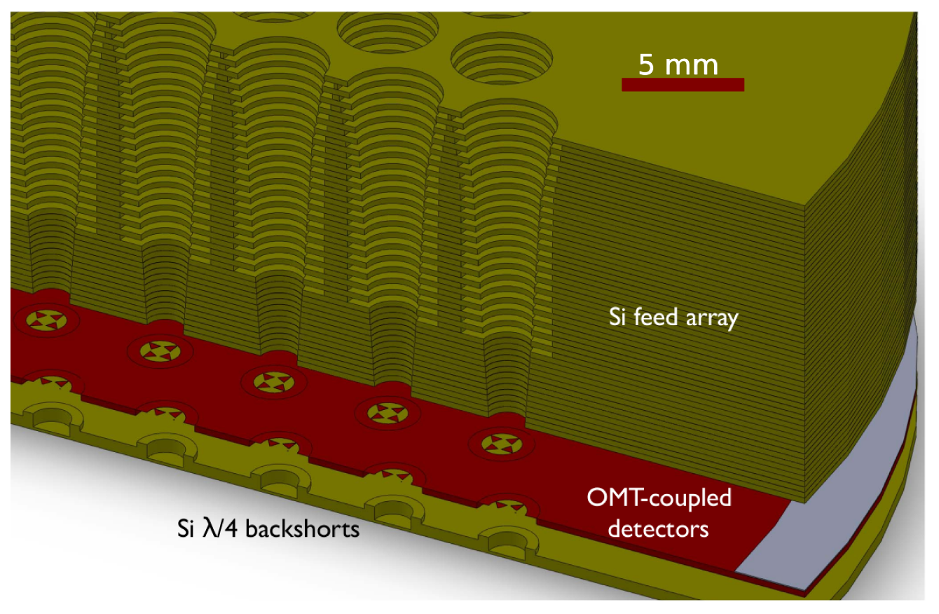
To demonstrate the feasibility of our approach, in 2009 we fabricated and tested two corrugated feeds made of Si.[14] Subsequently a prototype monolithic Si array of corrugated waveguides was also fabricated and tested. Currently underway at NIST is the fabrication of a diameter array with horns consisting of Si platelets. The platelets composing these devices were machined in mm and diameter Si wafers by use of photolithography and deep reactive ion etching (DRIE, see Appendix. A).
| 300 K | 300 K | 100 K | 293 K | 297 K | |
|---|---|---|---|---|---|
| Al | 2698 | 2.37 | 12.2 | 23.1 | 236 |
| Cu | 8933 | 3.39 | 10.3 | 16.5 | 403 |
| Si | 2329 | 1.58 | -0.4 | 2.6 | 168 (at 173 K) |
2 CORRUGATED FEED DESIGN


The prototype corrugated horn design is driven by the needs of the SPTpol and ACTpol receivers, both of which feature relatively fast optics at the focal plane (–). [12, 10] The input aperture diameter of the feed is determined by focal plane sensitivity calculations, optimizing the tradeoff between beam spillover efficiency and packing density. For the aforementioned receivers, simulations indicate an optimum clear aperture diameter of (center-to-center packing distance of accounting for the corrugation depths at the aperture), giving full width half maximum (FWHM) at nominal operation. The horn design follows standard practice. [8, 17] It was optimized over the band from GHz to GHz, appropriate for the GHz atmospheric window. The design was verified using a modal-matching simulation package (Microwave Wizard by Mician, GmbH).[18] See Fig. 2 for a schematic.
The design was tested experimentally by fabrication and measurement of a horn made from Si platelets each thick, each corresponding to a ridge or a groove of a corrugation (see Figure 2). A metal seed layer (Ti:Au:::) was deposited on the platelets mounted on an orbital platform canted at . Platelets were then stacked on stainless steel alignment pins, clamped with a jig and adhered at the edges with an electrically conductive epoxy. Platelet alignment accuracy by this approach was layer-to-layer.[14]
Subsequent electroplating of thick Cu followed by thick Au was performed to ensure a high-conductivity finish and to fill gaps between platelets ensuring electrical continuity. Note that the thickness of electrolytically deposited metals is systematically thinner in hard-to-reach high-aspect crevasses such as the corrugations near the center of the platelet array.[14] Cited thicknesses are as measured on flat, superficial surfaces. Electroplated copper was selected as an underlying layer due to its gap-filling properties. The Au plating thickness was selected to be well in excess of the skin depth of bulk Au: nm at GHz and .[16, 19].
3 FEED PERFORMANCE
A vector network analyzer (VNA) configured as described in Fig. 3 was used to characterize our horn’s return loss, insertion loss and far-field radiation patterns. The apparatus consisted of two horns: a fixed transmitter (Tx) and a receiver (Rx) that pivoted about the transmitting horn’s phase center. The Rx horn was a commercially manufactured corrugated metal horn for G-band (WR5). Simulated cross polarization is and side-lobe amplitude is dB at , and GHz. Return loss and insertion loss were measured with the horn aperture terminated against a microwave absorber or a shorting metal plate, respectively. To measure H-plane and E-plane beam patterns we used a or twist preceding the Tx and after the Rx horns. Cross polarization measurements used twists before the Tx horn and after the Rx horn. To confirm proper operation of the system we used a pair of identical metal horns in a test beam pattern measurement sweep. Manufacturing errors in the waveguide twists and our angle-sweeping setup limited the polarization aligment accuracy to , resulting in the leakage of the co-polar beam patterns dominating the nominal cross-polar beam pattern data at the level of dB; this represents an upper limit on the cross-polar levels of the prototype Si feed.
Figures 4, 5 and 6 show the measured return loss, insertion loss and far-field radiation pattern and cross polarization.
After the microwave measurements the horn was sliced in cross section on a dicing saw. This permitted inspection of the horn’s interior for micromachining, assembly and metalization defects. In particular we checked that the electroplated metal conformally coats sharp corners and bridges (fills) platelet-platelet gaps. Of inspected corners none were found without adequate metalization. Of inspected platelet-platlet junctions three were found with unsatisfactory coating of which only one which was certainly gapped.

4 SILICON FEED ARRAY
In late a prototype array structure with corrugated waveguides was fabricated, temperature cycled (to ) and tested on the VNA. Testing methods and performance were similar to the discrete Au-coated Si waveguides reported in .[14] Encouraged by the performance of this monolithic array of waveguides, we are now fabricating a diameter array with horns consisting of Si platelets (see Fig. 9).
For corrugated feeds it is necessary to use corrugations per .[8] Higher frequencies require thinner, more fragile wafers. However, thin, large diameter wafers are prone to fracture; handling mm diameter wafers thinner than is not desirable. To address this problem a two-tiered etch protocol was developed to permit the use of thicker wafers () each defining a full corrugation period. To reduce wafer handling the etch proceeded from a single side in two stages. See Figure 7 for a description of the Si platelet fabrication process and Figure 8 for images of Si platelets.
Typical wafer parameters for the Si used in the platelets are bulk resistivity (B doped, p-type), <100> crystal orientation (denoted by wafer flat), double-side polished ( nm rms), thickness and bow.
Individual platelets require metalization prior to stacking to facilitate subsequent electrolytic plating. Metal deposition by evaporation proved very robust in tests on individual feeds (Ti:Au:::) and will be used for monolithic arrays as well. As with the individual platelet feeds, platelet-platelet registration will be performed using (removable) stainless dowels and clearance holes micromachined in the Si. We are exploring use of epoxy and spring loaded clamps to ensure that the the gap between platelets is minimal during electroplating (Cu:Au:::).
5 CONCLUSION
We fabricated and tested Au-coated corrugated Si platelet waveguides, waveguide arrays and horns. These devices exhibited performance comparable to conventional all-metal devices. Our current work focuses on extending these techniques to fabrication of monolithic waveguide arrays with individual pixels on mm wafers.
The flexibility of Si micromachining makes possible a wide varity of microwave structures. For example, the 2-tiered etch recipe permits overlap of adjacent horns’ corrugations at the horn apertures for greater packing density. A 3-tiered etch makes posible “ring-loaded” corrugated horns with greatly increased spectral bandwidth for potential multichroic detectors.[20, 21]
APPENDIX A. SILICON DEEP ETCH
Plasma etching of silicon permits high aspect ratio features with good repeatability and excellent mask selectivity. The NIST etcher utilizes a variant of the BOSCH etch process optimized for silicon deep etch ().[22, 23] This process forms nearly vertical sidewalls in silicon by interleaving etch and surface passivation steps. The etch step is a chemically active RF plasma ( and ) inductively coupled to the wafer surface. The charged component of the plasma is accelerated normal to the surface, enhancing its etch rate in the vertical direction (tunable, ). The passivation step () coats all exposed surfaces including sidewalls with a fluorocarbon polymer. Etch and passivation cycles (typically and seconds respectively) are balanced so that sidewalls are protected from over/under etching as material is removed through the full wafer thickness. The cycled etching causes the sidewalls to have a microscopic scalloped appearance with an amplitude of and a period of .[23]
The primary etch mechanism for the / chemistry is due to chemical reactions between neutral atomic Fluorine formed in the plasma and silicon at the wafer surface. Oxygen acts to degrade the Fluorocarbon polymers () to form gaseous products. While other etch chemistries are possible, this is the most common owing to the safety of the reactants and their selectivity of silicon over commonly used etch masks (photoresist and silicon oxide).[24, 25] The gaseous products are pumped away and do not redeposit on the process wafer. Structures with multiple tiers per wafer are possible through the use of overlapping etch masks[26] or, at lower resolution, with roll-on photoresist.
DRIE permits fabrication of high-apect features in Si ( aspect ratio). Lateral resolution is limited by the greater of photolithography resolution and etch aspect ratio. For example, in thick Si the NIST etcher’s lateral resolution is through the full wafer bulk even though our photolithography resolution is . Radial variation in etch rate is ultimately determined by aspects of the DRIE etch tool such as plasma uniformity; we observe a radial (center to edge) variation of . Tools for applying this process to wafers in diameter are currently available in the NIST microfabrication facility. High resolution wafer-scale Si etch tools are ubiquitous in Si MEMs foundries.
ACKNOWLEDGMENTS
We thank the members of the ACT and SPT collaborations for their support and interest in this research. We thank John J. Jost and Dave Walker for suggestions on the manuscript. M. D. Niemack and K. W. Yoon acknowledge support from the National Research Council. This work was supported by NIST through the Innovations in Measurement Science program. This proceeding is a contribution of NIST and is not subject to U.S. copyright.


References
- [1] Bock, J. J., Gundersen, J., Lee, A. T., Richards, P. L., and Wollack, E., “Optical Coupling,” Journal of Physics: Conference Series 155, 012005 (2009).
- [2] Padin, S., Shepherd, M., Cartwright, J., Keeney, R., Mason, B., Pearson, T., Readhead, A., Schaal, W., Sievers, J., Udomprasert, P., et al., “The Cosmic Background Imager,” Publications of the Astronomical Society of the Pacific 114(791), 83–97 (2001).
- [3] Kovac, J., Leitch, E., Pryke, C., Carlstrom, J., Halverson, N., and Holzapfel, W., “Detection of Polarization in the Cosmic Microwave Background Using DASI,” Nature 420(6917), 772–787 (2002).
- [4] Barnes, C., Limon, M., Page, L., Bennett, C., Bradley, S., Halpern, M., Hinshaw, G., Jarosik, N., Jones, W., Kogut, A., Meyer, S., Motrunich, O., Tucker, G., Wilkinson, D., and Wollack, E., “The MAP Satellite Feed Horns,” The Astrophysical Journal Supplement Series 143(2), 567–576 (2002).
- [5] Jones, W. C., Bhatia, R., Bock, J. J., and Lange, A. E., “A Polarization Sensitive Bolometric Receiver for Observations of the Cosmic Microwave Background,” in [Millimeter and Submillimeter Detectors for Astronomy ], (2003).
- [6] Barkats, D., Bischoff, C., Farese, P., Gaier, T., Gundersen, J. O., Hedman, M. M., Hyatt, L., McMahon, J. J., Samtleben, D., Staggs, S. T., Stefanescu, E., Vanderlinde, K., , and Winstein, B., “Cosmic Microwave Background Polarimetry Using Correlation Receivers with the PIQUE and CAPMAP Experiments,” The Astrophysical Journal Supplement Series 159(1), 1–26 (2005).
- [7] Hinderks, J., Ade, P., Bock, J., Bowden, M., Brown, M., Cahill, G., Carlstrom, J., Castro, P., Church, S., Culverhouse, T. R. F., Ganga, K., Gear, W. K., Gupta, S., Harris, J., Haynes, V., Keating, B. G., Kovac, J., Kirby, E., Lange, A. E., Leitch, E., Mallie, O. E., Melhuish, S., Memari, Y., Murphy, A., Orlando, A., Schwarz, R., Sullivan, C. O., Piccirillo, L., Pryke, C., Rajguru, N., Rusholme, B., Taylor, A. N., Thompson, K. L., Tucker, C., turner, A. H., Wu, E. Y. S., and Zemcov, M., “QUaD: A High-Resolution Cosmic Microwave Background Polarimeter,” The Astrophysical Journal 692(2), 1221–1246 (2009).
- [8] Clarricoats, P. J. B. and Olver, A. D., [Corrugated Horns for Microwave Antennas ], IEEE Electromagnetic Waves Series (1984).
- [9] Lee, A. T., Tran, H., Ade, P., Arnold, K., Borrill, J., Dobbs, M. A., Errard, J., Halverson, N., Holzapfel, W. L., Howard, J., Jaffe, A., Keating, B., Kermish, Z., Linder, E., Miller, N., Myers, M., Niarchou, A., Paar, H., Reichardt, C., Spieler, H., Steinbach, B., Stompor, R., Tucker, C., Quealy, E., Richards, P. L., and Zahn, O., “POLARBEAR: Ultra-high Energy Physics with Measurements of CMB Polarization,” in [KEK Cosmophysics Group Inagural Conference - Accelerators in the Universe: Interplay Between High Energy Physcis and Cosmophysics ], Kodama, H. and Ioka, K., eds., 1040(1), 66–77, AIP (2008).
- [10] Niemack, M. D., “Actpol: A polarization-sensitive receiver for the atacama cosmology telescope,” in [Millimeter, Submillimeter, and Far-Infrared Detectors and Instrumentation for Astronomy V (Conference 7741) ], SPIE (2010).
- [11] Orlando, A., “Antenna-Coupled TES Bolometer Arrays for BICEP2/Keck and SPIDER,” in [Millimeter, Submillimeter, and Far-Infrared Detectors and Instrumentation for Astronomy V (Conference 7741) ], SPIE (2010).
- [12] Yoon, K. W., Appel, J., Austermann, J., Beall, J. A., Becker, D., Benson, B., Bleem, L., Britton, J. W., Carlstrom, J. E., Chang, C., Cho, H.-M., Crites, A., Essinger-Hileman, T., Everett, W., Halverson, N. W., Henning, J. W., Gene C. Hilton, K. D. I., McMahon, J. J., Mehl, J., Meyer, S. S., Moseley, S. H., Niemack, M. D., Parker, L. P., Simon, S., Staggs, S. T., and U-yen, K., “Feedhorn-Coupled TES Polarimeters for Next-Generation CMB Instruments,” in [Millimeter, Submillimeter, and Far-Infrared Detectors and Instrumentation for Astronomy V (Conference 7741) ], (2010).
- [13] Bock, J., Gundersen, J., Lee, A., Richards, P., and Wollack, E., “Optical Coupling,” Journal of Physics: Conference Series 155, 012005 (2009).
- [14] Britton, J., Yoon, K. W., Beall, J. A., Becker, D., Cho, H. M., Hilton, G. C., Niemack, M. D., and Irwin, K. D., “Progress Toward Corrugated Feed Horn Arrays in Silicon,” in [The Thirteenth International Workshop on Low Temperature Detectors - LTD13 ], Young, B., Cabrera, B., and Miller, A., eds., 1185(1), 375–378, AIP (2009).
- [15] Yoon, K. W., Appel, J. W., Austermann, J. E., Beall, J. A., Becker, D., Benson, B. A., Bleem, L. E., Britton, J., Chang, C. L., Carlstrom, J. E., Cho, H.-M., Crites, A. T., Essinger-Hileman, T., Everett, W., Halverson, N. W., Henning, J. W., Hilton, G. C., Irwin, K. D., McMahon, J., Mehl, J., Meyer, S. S., Moseley, S., Niemack, M. D., Parker, L. P., Simon, S. M., Staggs, S. T., U-yen, K., Visnjic, C., Wollack, E., and Zhao, Y., “Feedhorn-Coupled TES Polarimeters for Next-Generation CMB Instruments,” in [The Thirteenth International Workshop on Low Temperature Detectors - LTD13 ], Young, B., Cabrera, B., and Miller, A., eds., 1185(1), 515–518, AIP (2009).
- [16] Kaye, G. W. C. and Laby, T. H., [Tables of Physical and Chemical Constants ] (2009).
- [17] Granet, C. and James, G., “Design of Corrugated Horns: A Primer,” Antennas and Propagation Magazine, IEEE 47, 76–84 (April 2005).
- [18] “Products or companies named here are cited only in the interest of complete technical description, and neither constitute nor imply endorsement by NIST or by the US government. Other products may be found to serve just as well.”
- [19] Jackson, J. D., [Classical Electrodynamics ], Wiley, New York, 3rd ed ed. (1999).
- [20] McMahon, J. private correspondence (2009).
- [21] Takeichi, Y., Hashimoto, T., and Takeda, F., “The Ring-Loaded Corrugated Waveguide,” in [Microwave Symposium Digest, GMTT International ], 71(1), 36–37 (1971).
- [22] Larmer, F. and Schilp, A., “Method for anisotropically etching silicon.” German Patent DE4241045 (1992).
- [23] McAuley, S. A., Ashraf, H., Atabo, L., Chambers, A., Hall, S., Hopkins, J., and Nicholls, G., “Silicon Micromachining Using a High-Density Plasma Source,” Journal of Physics D-Applied Physics 34, 2769–2774 (2001).
- [24] Flamm, D. L., “Mechanisms of Silicon Etching in Fluorine-Containing and Chlorine-Containing Plasmas,” Pure Appl. Chem. 62, 1709–1720 (1990).
- [25] Madou, M. J., [Fundamentals of Microfabrication : The Science of Miniaturization ], CRC Press, Boca Raton, 2nd ed ed. (2002).
- [26] Britton, J., Leibfried, D., Beall, J. A., Blakestad, R. B., Wesenberg, J. H., and Wineland, D. J., “Scalable Arrays of RF Paul Traps in Degenerate Si,” Applied Physics Letters 95(17), 173102 (2009).