Electronic-Structure-Driven Magnetic Ordering in a Kondo Semiconductor CeOs2Al10.
Abstract
We report the anisotropic changes in the electronic structure of a Kondo semiconductor CeOs2Al10 across an anomalous antiferromagnetic ordering temperature () of 29 K, using optical conductivity spectra. The spectra along the - and -axes indicate that a - hybridization gap emerges from a higher temperature continuously across . Along the -axis, on the other hand, a different energy gap with a peak at 20 meV appears below 39 K, which is higher temperature than , because of structural distortion. The onset of the energy gap becomes visible below . Our observation reveals that the electronic structure as well as the energy gap opening along the -axis due to the structural distortion induces antiferromagnetic ordering below .
pacs
71.27.+a, 78.20.-eRare-earth intermetallic compounds provide useful materials with characteristic physical properties, such as heavy fermions, Kondo semiconductors/insulators, and so on, due to the interaction between the local electrons and the conduction electrons; namely - hybridization [1]. With regard to these properties, Kondo semiconductors are known to have a - hybridization gap on the Fermi level (), even though the magnetic susceptibility at high temperature obeys the Curie-Weiss law, indicating the local character [2]. Typical Kondo semiconductors such as SmB6, YbB12, Ce3Bi4Pt3, CeRhSb, and others studied previously have no phase transition below the Kondo temperature () because the magnetic moments of Ce are quenched due to the Kondo singlet state via strong - hybridization.
However, the recently discovered Kondo semiconductors CeAl10 ( = Os, Ru) that show another anomalous phase transition at a characteristic temperature (28.7 K for = Os, 27.3 K for Ru) below the Kondo temperature (100 K for Os, 60 K for Ru) have been found [3, 4, 5], in contrast to the related material CeFe2Al10, which is a typical Kondo semiconductor even at very low temperatures [6, 7]. Below , CeOs2Al10 shows a different semiconducting activation type electrical resistivity from that above despite the fact that CeRu2Al10 shows metallic characteristics [8]. CeAl10 is an orthorhombic YbFe2Al10 type crystal structure (space group , No. 63) [9]. Very recently, long-range antiferromagnetic ordering with small magnetic moments has been observed below in CeOs2Al10 and CeRu2Al10 [12, 11, 13]. Since the Ce–Ce distance is about 5 Å, which is longer than that of normal Ce compounds, however, the Ruderman-Kittel-Kasuya-Yoshida (RKKY) interaction is not believed to be the origin of the phase transition at . Therefore, the origin of the antiferromagnetic ordering remains unknown.
In this Letter, we describe an investigation into the origin of the anomalous phase transition at , as well as the change in the electronic structure of CeOs2Al10, using temperature-dependent anisotropic optical conductivity [] spectra. At higher temperatures, CeOs2Al10 has the electronic structure of an anisotropic semiconductor. Below 39 K (hereafter, ), which is higher than , on the other hand, a pronounced peak structure of the spectra only along the -axis appears at a photon energy of 20 meV, indicating evolution of the energy gap because of structural distortion; the spectra along the - and -axes are unchanged, except for a reduction in thermal broadening. Onset of the 20-meV peak appears below . These observations indicate that opening of the energy gap induces antiferromagnetic ordering.
Near-normal incident polarized optical reflectivity [] spectra were acquired in a very wide photon-energy region of 2 meV – 30 eV to ensure an accurate Kramers-Kronig analysis (KKA). Single-crystalline CeOs2Al10 was synthesized by the Al-flux method [8] and was well-polished using 0.3 m grain-size Al2O3 wrapping film sheets for the measurements. Martin-Puplett and Michelson type rapid-scan Fourier spectrometers (JASCO Co. Ltd., FARIS-1 and FTIR610) were used at photon energies of 2 – 30 meV and 5 meV – 1.5 eV, respectively, with a specially designed feed-back positioning system to maintain the overall uncertainty level less than 0.5 % at sample temperatures in the range of 8 – 300 K [14]. To obtain the absolute values, the samples were evaporated in-situ with gold, whose spectrum was then measured as a reference. At K, was measured for energies 1.2–30 eV by using synchrotron radiation [15]. In order to obtain via KKA of , the spectra were extrapolated below 2 meV with a Hagen-Rubens function, and above 30 eV with a free-electron approximation [16].

The spectra obtained along the -axis (), -axis (), and -axis () are shown in Fig. 1. As can be seen in the inset, the spectra monotonically decrease up to = 10 eV because the conduction band of Al expands to about 10 eV below according to the band calculation (not shown). The characteristic double-peak structure of Ce compounds in the energy range of 100–300 meV, which originates from the top of the valence band to the unoccupied Ce state with spin-orbit splitting [17], slightly appears only in . In addition, the X-ray photoemission spectrum of the Ce core level suggests mixed valence of the Ce ion (not shown) [18]. Both of these features indicate strong - hybridization intensity.
Let us focus on the spectra below 100 meV. There are two sharp peaks in , one peak in , and three peaks in in the range = 10–25 meV due to optical phonons. Except for these peaks, the spectra for all principal axes at 300 K are Drude-like spectra that increase to unity with decreasing photon energy, indicating a metallic character. Below 80 K, the value of below 50 meV rapidly decreases with decreasing temperature, and eventually, at the lowest accessible photon energy, does not close to unity at 8 K except for . This indicates the existence of an energy gap; i.e., the material changes to an insulator.

The temperature-dependent spectra derived from KKA of the spectra in Fig. 1 are shown in Fig. 2. The spectra for all principal axes at 300 K monotonically increase with decreasing photon energy, again indicating a metallic character. Commonly in all principal axes, the intensity below = 60 meV decreases with decreasing temperature, and at 80 K, a broad shoulder structure appears at about 45 meV, which indicates the energy gap due to the strong - hybridization similar to other Kondo semiconductors [19, 20, 21, 22].
In and , the gentle shoulder structures at about 50 meV at 80 K gradually evolve below 130 K and an energy-gap structure appears at the low-energy side of the peak as the temperature decreases to the minimum. However, the gap shape and energy do not change with temperature (except for the reduction in thermal broadening), unlike the case in . Below 40 K, a sharp Drude structure appears below 10 meV that differs from the spectral shape above 80 K. Therefore, the gap structure drastically changes at around . At 8 K, the Drude structure disappears in the spectral range and a clear energy gap opens, despite the fact that the direct current conductivity along the -axis is about 4000 to 3000 cm-1 in all temperature regions. This means that a very narrow Drude peak due to in-gap states must appear below the accessible energy region. The origin of the in-gap states is not clear at present.

In , the overall temperature dependence is similar to those in and , but one peak at and an energy gap below 20 meV suddenly appear at temperatures between 20 and 40 K. To assist in studying the spectral change in detail, Figs. 3(a)–(c) show the fine temperature dependence ( 2 K) of the spectra at temperatures from 10 to 40 K in the three principal axes. With decreasing temperature, the spectral weight below 10 meV decreases in and . The temperature dependence of the intensity at 5 meV is plotted as for and for in Fig. 3(d). Both and monotonically decrease with decreasing temperature and do not show anomalies at . The temperature dependence is the same as that of typical Kondo semiconductors [19, 20, 21, 22], i.e., the state in and can be regarded as that of a Kondo semiconductor.
In , on the other hand, not only does the spectral weight below 10 meV decrease, but also a peak grows at 20 meV with decreasing temperature. As seen in the and behavior, the spectral weight shifts from the lower to the higher energy side across the energy gap. The change starts at about , not . is the temperature of maximum magnetic susceptibility () and of the upturn in electrical resistivity () [8]. Therefore, the downturn in and upturn in originate from generation of the 20-meV peak. In addition, the drastic change in the electronic structure in is consistent with the finding that the temperature-dependent in at around is the largest among those of all the principal axes.
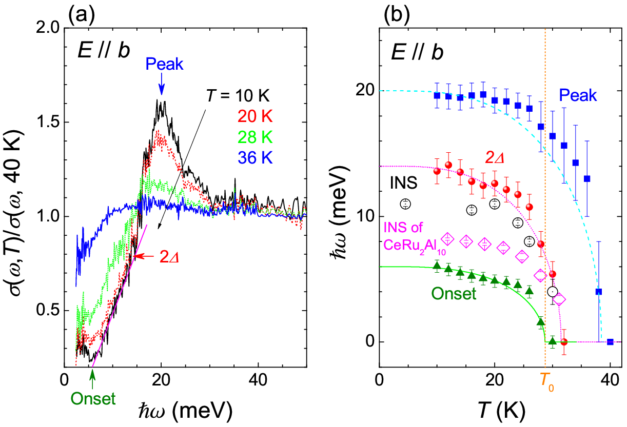
To clarify the difference in temperature dependence of the spectra in , the ratio [] spectra, i.e., at a given temperature divided by that at 40 K, are shown in Fig. 4(a). These plots clearly demonstrate the transfer of the spectral weight across and . In the figure, a peak that appears at 20 meV at 10 K shifts to the low energy side and broadens with increasing temperature. From the temperature-dependent peak structure, the peak energy, the energy at the half-peak intensity (), and the onset of the gap are plotted as a function of temperature in Fig. 4(b). In the same way as in Fig. 3(d), the peak is generated below and does not have an anomaly at . However, the onset becomes visible below . These results mean that the electronic structure is modulated below and the energy gap fully opens below . At , antiferromagnetic ordering is developed. This indicates that the magnetic phase transition is driven by the electronic structure as well as the energy-gap opening in . The gap size , indicated by the solid circles in Fig. 4(b), develops below a slightly higher temperature than . The temperature dependence of is consistent with the peak of inelastic neutron scattering (INS) of the same material and the related material CeRu2Al10 with the temperature normalized by [12, 13]. In the figure, the temperature dependence of the superconducting gap predicted by BCS theory is also plotted for reference. The temperature dependence at all data points is similar to, but deviates slightly from, the BCS curves. This result is consistent with the previous study of charge-density wave (CDW) and spin-density wave (SDW) transitions such as that of (TMTSF)2PF6 [23]. In the case of CeOs2Al10, no magnetic transition was observed at . Therefore, CDW is more plausible for the origin of . This is consistent with the observed superlattice reflections along the direction [8].
The change in the spectrum due to the CDW and SDW transitions has previously been studied experimentally in -TiSe2 [24], P4W14O50 [25], (TMTSF)2PF6 [23], Cr [26], and others. In all cases, the data obtained have indicated that the gap size is significantly larger than the mean-field BCS value of , where is the critical temperature (). In the case of CeOs2Al10, can be regarded as . Because at 10 K is 141.2 meV ( K), the relationship between and becomes . This is consistent with the results of previous studies. Therefore, the CDW scenario is again supported.
To summarize, the electronic structure and origin of the anomalous phase transition of CeOs2Al10 were investigated by the measurement of temperature-dependent polarized optical conductivity spectra. Along the - and -axes, the spectral weight at energies lower than 10 meV monotonically decreased with decreasing temperature, indicating a Kondo semiconductor characteristic with an energy gap of about 10 meV realized in all temperatures. In contrast, along the -axis, a CDW energy gap opened below 39 K, which is higher than , and the onset of the energy gap become visible at . Therefore, the anomalous antiferromagnetic transition at is concluded to be driven by CDW transition along the -axis, in contrast to the lack of phase transition along the - and -axes.
We would like to thank Mr. Hajiri for his help of Ce XPS measurement. Part of this work was supported by the Use-of-UVSOR Facility Program (BL7B, 2009) of the Institute for Molecular Science. The work was partly supported by a Grant-in-Aid for Scientific Research from MEXT of Japan (Grant No. 22340107, 20102004).
References
- [1] A. C. Hewson, The Kondo Problem to Heavy Fermions (Cambridge University Press, Cambridge, 1993).
- [2] T. Takabatake, F. Iga, T. Yoshino, Y. Echizen, K. Katoh, K. Kobayashi, M. Higa, N. Shimizu, Y. Bando, G. Nakamoto, H. Fujii, K. Izawa, T. Suzuki, T. Fujita, M. Sera, M. Hiroi, K. Maezawa, S. Mock, H. v. Löhneysen, A. Brückl, K. Neumaier, and K. Andres, J. Magn. Magn. Mater. 177-181, 277 (1998), and references therein.
- [3] A. M. Strydom, Physica B 404, 2981 (2009).
- [4] T. Nishioka, Y. Kawamura, T. Takesaka, R. Kobayashi, H. Kato, M. Matsumura, K. Kodama, K. Matsubayashi, and Y. Uwatoko, J. Phys. Soc. Jpn. 78, 123705 (2009).
- [5] M. Matsumura, Y. Kawamura, S. Edamoto, T. Takesaka, H. Kato, T. Nishioka, Y. Tokunaga, S. Kambe, and H. Yasuoka, J. Phys. Soc. Jpn. 78, 123713 (2009).
- [6] Y. Muro, K. Motoya, Y. Saiga, and T. Takabatake, J. Phys. Soc. Jpn. 78, 083707 (2009).
- [7] Y. Muro, K. Motoya, Y. Saiga, and T. Takabatake, J. Phys.: Conf. Ser. 200, 012136 (2010).
- [8] Y. Muro, J. Kajino, K. Umeo, K. Nishimoto, R. Tamura, and T. Takabatake, Phys. Rev. B 81, 214401 (2010).
- [9] V. M. T. Thiede, T. Ebel, and W. Jeitschko, J. Mater. Chem. 8, 125 (1998).
- [10] T. Takesaka, K. Oe, R. Kobayashi, Y. Kawamura, T. Nishioka, H. Kato, M. Matsumura, and K. Kodama, J. Phys.: Conf. Ser. 200, 012201 (2010).
- [11] D. D. Khalyavin, A. D. Hillier, D. T. Adroja, A. M. Strydom, P. Manuel, L. C. Chapon, P. Peratheepan, K. Knight, P. Deen, C. Ritter, Y. Muro, and T. Takabatake, Phys. Rev. B 82, 100405(R) (2010).
- [12] D. T. Adroja, A. D. Hillier, P. P. Deen, A. M. Strydom, Y. Muro, J. Kajino, W. A. Kockelmann, T. Takabatake, V.K. Anand, J.R. Stewart, and J. Taylor, Phys. Rev. B 82, 104405 (2010).
- [13] J. Robert, J. -M. Mignot, G. André, T. Nishioka, R. Kobayashi, M. Matsumura, H. Tanida, D. Tanaka, and M. Sera, Phys. Rev. B 82, 100404(R) (2010).
- [14] S. Kimura, JASCO Report 50, 6 (2008). [in Japanese]
- [15] K. Fukui, H. Miura, H. Nakagawa, I. Shimoyama, K. Nakagawa, H. Okamura, T. Nanba, M. Hasumoto, and T. Kinoshita, Nucl. Instrum. Methods Phys. Res. A 467-468, 601 (2001).
- [16] M. Dressel and G. Grüner, Electrodynamics of Solids (Cambridge University Press, Cambridge, UK, 2002).
- [17] S. Kimura, T. Iizuka, and Y. S. Kwon, J. Phys. Soc. Jpn. 78, 013710 (2009).
- [18] H. Miyazaki, T. Hajiri, Y. Muro, T. Takabatake, and S. Kimura, unpublished data.
- [19] S. Kimura, T. Nanba, S. Kunii, and T. Kasuya, Phys. Rev. B 50, 1406 (1994).
- [20] B. Bucher, Z. Schlesinger, P. C. Canfield, and Z. Fisk, Phys. Rev. Lett. 72, 522 (1994).
- [21] H. Okamura, S. Kimura, H. Shinozaki, T. Nanba, F. Iga, N. Shimizu, and T. Takabatake, Phys. Rev. B 58, R7496 (1998).
- [22] M. Matsunami, H. Okamura, T. Nanba, H. Sugawara, and H. Sato, J. Phys. Soc. Jpn. 72, 2722 (2003).
- [23] M. Dressel, L. Degiorgi, J. Brickmann, A. Schwartz, and G. Grüner, Physica B 230-232, 1008 (1997).
- [24] G. Li, W. Z. Hu, D. Qian, D. Hsieh, M. Z. Hasan, E. Morosan, R. J. Cava, and N. L. Wang, Phys. Rev. Lett. 99, 027404 (2007).
- [25] Z. -T. Zhu, J. L. Musfeldt, Z. S. Teweldemedhim, and M. Greenblatt, Phys. Rev. B 65, 214519 (2002).
- [26] A. S. Barker, Jr., B. I. Halperin, and T. M. Rice, Phys. Rev. Lett. 20, 384 (1968).