Perpendicular anisotropy of ultrathin epitaxial cobalt films on graphene
Abstract
Graphene is attractive for spintronics due to its long spin life time and high mobility. So far only thick and polycrystalline slabs have been used as ferromagnetic electrodes. We report the growth of flat, epitaxial ultrathin Co films on graphene. These display perpendicular magnetic anisotropy in the thickness range , which is confirmed by theory. PMA, epitaxy and ultrathin thickness bring new perspectives for graphene-based spintronic devices such as the zero-field control of an arbitrary magnetization direction, band matching between electrodes and graphene, and interface effects such as Rashba and electric field control of magnetism.
While graphite exfoliation provides flakes of graphene of lateral size limited to at most [1], the epitaxial synthesis on SiC[2] or metals[3, 4] allows for the batch and large-area availability and processing[5] of single and multi-layer graphene. Since 2009 the CVD route is no longer restricted to supports made of metallic single crystals, but was extended to thin films such as Ni[6, 7] or Cu[8], in sheets or deposited on various supporting surfaces. The main motivation so far comes from the demonstrated possibility to finally strip off the metal support for the use of the bare graphene sheet in applications, e.g. concerning electronic transport or photovoltaics.
So far devices have relied on electrodes made with standard clean-room facilities, yielding thick and grainy electrodes, and thus a poor control of the microstructure, electronic band matching with graphene, and control over magnetism. This remains far beyond the state-of-the art surface-science engineering developed for epitaxial metal-on-metal ferromagnetic systems. In this Letter we report the optimization of the epitaxial growth of Au-capped Co ultrathin films on graphene. These are found to display perpendicular magnetic anisotropy (PMA) in the thickness range . Theory reveals an active role of the Co/graphene interface in sustaining PMA. The high uniformity of the layers is confirmed by the exceptionally-low coercivity () over the entire PMA range, suitable for the reliable control of magnetization via magnetic or electric fields. These features open new perspectives for both free-standing or hererostructure-based graphene devices.
The synthesis was conducted in ultra-high vacuum (base pressure )[9]. The metallic layers were grown by pulsed laser deposition (PLD)[10] using a Nd-YAG laser with doubled frequency. A computer-controlled mask can be moved in front of the wafer for producing wedge-shaped samples. Details can be found in [9]. CVD is performed with ethylene molecules provided by a dosing tube facing the sample, with a partial pressure of measured in the chamber. The samples were grown on Sapphire-C wafers supplied by Roditi Ltd. (miscut angle or depending on the batch), which were outgassed twice in situ under UHV at 850 ∘C during 45 min. in situ scanning tunneling microscopy (STM-1 Omicron) and reflection high energy electron diffraction (RHEED, Riber 10 keV) were used. High resolution transmission electron microscopy (TEM) was conducted ex situ with a JEOL 4000EX setup with an acceleration voltage of . The cross-sectional specimens were thinned by mechanical grinding and ion milling using a PIPS system. Magnetization reversal was probed using the Magneto-Optical Kerr Effect (MOKE). Hysteresis loops were gathered at with a laser spot of a few microns and incidence away from the normal to the plane. A commercial MOKE microscope from Evico-magnetics was also used, with an image in the saturation state subtracted from all images. In both cases we are essentially sensitive to perpendicular magnetization (polar MOKE), and the applied field is perpendicular to the plane. The extraordinary Hall effect (EHE) was measured at room temperature in a four-probe geometry. For first principle calculations we used the Vienna ab initio simulation package (VASP)[11] based on the DFT with the generalized gradient approximation [12] and projector augmented wave[13]. The Magnetic Anisotropy Energy (MAE) was calculated in two steps. First, the Kohn-Sham equations were solved with no spin-orbit interaction allowing for an out-of-plane structural relaxation. Then the spin-orbit coupling was included and the total energy of the system was determined as function of the orientation of the magnetic moments. The MAE is computed as the difference between the in-plane and out-of-plane total energy values.
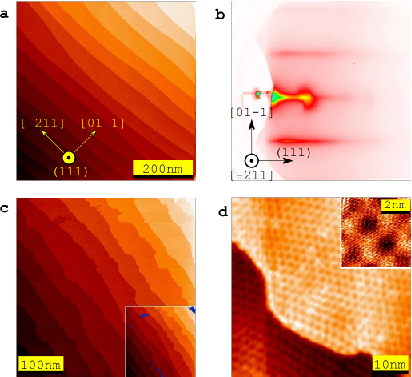
The experimental stack is . Ir is deposited at 430 ∘C and annealed at during 30 min. This yields epitaxial Ir(111) with atomically flat terraces whose width is only limited by the miscut angle of the wafer (Figure 1a-b)[14]. CVD of graphene on top of Ir is self-limited to a single complete layer of graphene similarly to the growth on Ir single crystals[15] (Figure 1c-d). The graphene replicates the atomic smoothness of the Ir(111) buffer layer by extending coherently across its atomic steps.
The growth at room temperature (RT) of Co on graphene proceeds nearly perfectly layer-by-layer up to about (Figure 2a)[16]. For larger thicknesses the roughness progressively increases. In both cases the annealing of the deposit at yields a flat Co film, with a mean terrace width again only limited by the miscut angle of the wafer (Figure 2b). The stacking is finally terminated with a -thick RT Au deposit. TEM confirms the smoothness and uniformity of the Co layer (Figure 2c). The Co layer is mainly hexagonal compact (its stable RT bulk structure) however with locally stacking faults and/or face-centered-cubic (stable above in the bulk, however often stabilized in nanostructures) crystals (Figure 2h). The graphene sheet cannot be identified on these images due to the graphene-Co spacing being similar to that of Co-Co[17]. The in-plane epitaxial relationships is .

Let us first discuss the MAE of these films. In the uniaxial case the density of MAE is described to first order as with in units of . With the angle between the magnetization and the normal to the film, positive values of mean perpendicular magnetic anisotropy (PMA), while negative values mean alignment of magnetization in the plane. Our hysteresis loops provide evidence for PMA in the range of thickness (Figure 3a). Let us recall that in most magnetic films the magnetization is strongly constrained to lie in-the-plane, due to the negative contribution of the magnetostatic energy to the MAE. PMA may be achieved only for selected cases where the magnetostatic energy is overcome by positive contributions to the MAE. In ultrathin films PMA may result from interface and/or magneto-elastic effects[18]. As both terms decay essentially like with the film thickness, PMA is restricted to thicknesses typically below . Known ultrathin stackings with PMA are either all metal-based[19] or metal-oxide based[20]. In a first approach Au/Co/graphene may be discussed in the view of existing data for the Co-Au interface. This interface favors PMA with a magnitude [19], such that full PMA is maintained up to for two such interfaces. PMA is maintained up to in our case, so that we expect the contribution of the Co/graphene interface to the PMA to be of similar magnitude.
We used first-principle calculations to highlight the role in PMA of the Co/graphene, were a significant subtly on strain and local environment, the structural details of the Co slab and its interfaces should be taken into account accurately for a quantitative discussion. However while Co and graphene have very similar lattice parameters, a large in-plane lattice mismatch exists between Au and Co () and Ir and Co/graphene (). As a consequence a discommensuration moiré pattern exists at both interfaces of the Co/graphene slab, each with a pitch of a few nanometers, and incommensurate one with another. Thus any approximant unit cell for the realistic stacking would be at least ten nanometers in lateral size, which is far out of reach of first principle calculations. Alternatively, considering highly strained Ir and Au layers to avoid the moiré would be physically unrealistic. With a view to highlighting the physics at the novel Co/graphene interface we compared two simple and tractable cases, that of two slabs of thickness three atomic layers of hexagonal compact Co, either free standing or in contact with a commensurate graphene sheet on one side (Figure 4). vacuum was added on each side with periodic boundary conditions, and were used. The most stable structural arrangement with graphene was found to be that with carbon atoms sitting right atop the Co atoms of the uppermost layer (Figure 4), with an interface distance of after out-of-plane relaxation, consistent with existing results[17]. Both systems exhibit a strong PMA, equalling for the free-standing slab, and for the graphene-capped slab; both figures include the magnetostatic contribution amounting to for this thickness. This means that in this ultrathin range the Co/graphene interface plays an active role in promoting PMA, with a strength of the order of , of a similar order of magnitude than that expected from the crude arguments given in the previous paragraph.

We now discuss magnetization reversal. The coercive field is of the order of a few mT (Figure 3a-b). This is several orders of magnitude smaller than the anisotropy field, whose lower bound was estimated to using EHE. This suggests[21] that magnetization reversal proceeds by the nucleation of a few reversed domains at defects of the extended film, followed by an easy propagation of domain walls. The confirmation is gained through the monitoring of magnetic domains during magnetization reversal, using Kerr microscopy. Under quasistatic conditions the average size of the domains is larger than one hundred micrometers (Figure 3c), and magnetization reversal proceeds solely through the propagation of domain walls (see also the Kerr movie as supplementary material, real-time, ). Low coercivity is usually difficult to achieve in PMA materials because their MAE is large by nature. Similar weak pinning and has been demonstrated in selected metal-on-metal systems, however in the very special cases where magnetism is weakened by either selecting extremely low thickness[22] or by weakening anisotropy and magnetism by ion irradiation[23]. For Co/graphene low coercivity is maintained through the entire range of thickness for PMA, which points at the intrinsic quality and homogeneity of the layer.

We finally discuss outlooks. There is no reason why growth and magnetic features would differ for other sources of graphene, e.g. on SiC[2], exfoliated[1] or reported on-metal CVD[6, 7, 8]. Free of a conducting buffer layer, these are a priori better suited for lateral transport devices. For these lateral devices PMA would ensure that full remanence, low magnetostatic interactions thanks to the ultrathin thickness, and high thermal stability thanks to the high MAE, may be achieved for nanostructures down to very small lateral sizes, required e.g. for making use of the short-range RKKY coupling[24]. Bringing zero-field perpendicular magnetization, PMA also opens the door to the easy realization of devices with cross-magnetized electrodes such as those needed for efficient spin-transfer torque magnetization precession. Besides, whereas most studied so far considered on spin transport through bare graphene between lateral ferromagnetic electrodes, graphene embedded in a metal stack displays specific features whose interest have not been exploited yet. For example a graphene/Co/graphene stack embedded within metal weakly bonded with graphene[17] may provide a way to decouple the conduction channels in each layer, and thus ensure a highly spin-polarized conduction channel through Co. This may solve the issue of the loss of effective spin polarization in all-metal stacks with PMA investigated for the current-induced propagation of domain walls[25]. Other graphene-relevant interfacial effects pertain to novel ways of controlling magnetization, such as Rashba spin-orbit coupling[26] and electric-fields[27]. The use of ultrathin layers is crucial for these interface-based physics so that the relative effects are large. Finally, epitaxial samples are also desirable in this case to achieve a good and uniform matching of electronic bands, for engineering the effects and also provide simple cases for their fundamental understanding.
To conclude we have developed Au-capped atomically-smooth ultrathin epitaxial Co films on graphene by combining CVD and PLD, which display perpendicular magnetic anisotropy (PMA) in the range of thickness . The availability of such electrodes broadens the spectrum of graphene-based devices that can be realized, either for ultra-small lateral sizes or cross-magnetization electrodes with PMA, or new interface-based physics in graphene hybrid stackings such as Rashba or electric field control of magnetism.
References
References
- [1] K. S. Novoselov, A. K. Geim, S. V. Morozov, D. Jiang, Y. Zhang, S. V. Dubonos, I. V. Grigorieva, and A. A. Firsov, Science 306, 666 (2004).
- [2] K. V. Emtsev, A. Bostwick, K. Horn, J. Jobst, G. L. Kellogg, L. Ley, J. L. McChesney, T. Ohta, S. A. Reshanov, J. R. E. Rotenberg, A. K. Schmid, D. Waldmann, H. B.Weber, and T. Seyller, Nat. Mater. 8, 203 (2009).
- [3] J. Coraux, A. T. N’Diaye, C. Busse, and T. Michely, Nano Lett. 8, 565 (2008).
- [4] P. W. Sutter, J. I. Flege, and E. A. Sutter, Nat. Mater. 7, 406 (2008).
- [5] N. Tombros, C. Jozsa, M. Popinciuc, H. T. Jonkman, and B. J. van Wees, Nature 448, 571 (2007).
- [6] A. Reina, X. Jia, J. Ho, D. Nezich, H. Son, V. Bulovic, M. S. Dresselhaus, and J. Kong, Nano Lett. 9, 30 (2009).
- [7] K. S. Kim, Y. Zhao, H. Jang, S. Y. Lee, J. M. Kim, K. S. Kim, J.-H. Ahn, P. Kim, J.-Y. Choi, and B. H. Hong, Nature 457, 706 (2009).
- [8] X. Li, W. Cai, J. An, S. Kim, J. Nah, D. Yang, R. Piner, A. Velamakanni, I. Jung, E. Tutuc, S. K. Banerjee, L. Colombo, and R. S. Ruoff, Science 324, 1312 (2009).
- [9] O. Fruchart, M. Eleoui, P. O. Jubert, P. David, V. Santonacci, F. Cheynis, B. Borca, M. Hasegawa, and C. Meyer, J. Phys.: Condens. Matter 19, 053001 (2007).
- [10] J. Shen, Z. Gaib, and J. Kirschner, Surf. Sci. Rep. 52, 163 (2004).
- [11] G. Kresse and J. Furthmüller, Phys. Rev. B 54, 11169 (1996).
- [12] J. P. Perdew, J. A. Chevary, S. H. Vosko, K. A. Jackson, M. R. Pederson, D. J. Singh, and C. Fiolhais, Phys. Rev. B 46, 6671 (1992).
- [13] P. E. Blöchl, Phys. Rev. B 50, 17953 (1994).
- [14] C. Vo-Van, J. Coraux, and O. Fruchart, unpublished.
- [15] J. Coraux, A. T N’Diaye, M. Engler, C. Busse, D. Wall, N. Buckanie, F.-J. Meyer zu Heringdorf, R. van Gastel, B. Poelsema, and T. Michely, New J. Phys. 11, 023006 (2009).
- [16] At RT the reported growth on graphene/Ir of transition metals such as Fe[28] or Ni[29] proceeds in the form of dilute assemblies of multi-layered clusters. Only deposits thicker than several atomic layers or even nanometers monolayers are expected to yield a continuous film. Here instead of MBE we use PLD, whose higher instantaneous deposition rate and thus higher nucleation rate, is known to favor layer-by-layer growth[10, 30].
- [17] G. Giovannetti, P. A. Khomyakov, G. Brocks, V. M. Karpan, J. van den Brink, and P. J. Kelly, Phys. Rev. Lett. 101, 026803 (2008).
- [18] Here we leave aside those cases where positive contributions to the MAE arise from bulk magnetocrystalline anisotropy such as for rare-earth-3d, FePt, CoPt.
- [19] M. T. Johnson, P. J. H. Bloemen, F. J. A. den Broeder, and J. J. de Vries, Rep. Prog. Phys. 59, 1409 (1996).
- [20] B. Rodmacq, A. Manchon, C. Ducruet, S. Auffret, and B. Dieny, Phys. Rev. B 79, 024423 (2009).
- [21] D. Givord, M. Rossignol, and V. M. T. S. Barthem, J. Magn. Magn. Mater. 258-259, 1 (2003).
- [22] J.-C. Lee, K.-J. Kim, J. Ryu, K.-W. Moon, S.-J. Yun, G.-H. Gim, K.-S. Lee, K.-H. Shin, H.-W. Lee, and S.-B. Choe (2010).
- [23] C. Chappert, H. Barnas, J. Ferré, V. Kottler, J.-P. Jamet, Y. Chen, E. Cambril, T. Devolder, F. Rousseaux, V. Mathet, and H. Launois, Science 280, 1919 (1998).
- [24] J. E. Bunder and H.-H. Lin, Phys. Rev. B 80, 153414 (2009).
- [25] M. Cormier, A. Mougin, J. Ferré, A. Thiaville, N. Charpentier, F. Piéchon, R. Weil, V. Baltz, and B. Rodmacq, Phys. Rev. B 81, 024407 (2010).
- [26] I. M. Miron, G. Gaudin, S. Auffret, B. Rodmacq, A. Schuhl, S. Pizzini, J. Vogel, and P. Gambardella, Nat. Mater. 9, 230 (2010).
- [27] M. Weisheit, S. Fähler, A. Marty, Y. Souche, C. Poinsignon, and D. Givord, Science 315, 349 (2007).
- [28] A. T. N’Diaye, T. Gerber, C. Busse, J. Myslivecek, J. Coraux, and T. Michely, New J. Phys. 11, 103045 (2009).
- [29] M. Sicot, S. Bouvron, O. Zander, U. Rüdiger, Y. S. Dedkov, and M. Fonin, Appl. Phys. Lett. 96, 093115 (2010).
- [30] C. Clavero, A. Cebollada, G. Armelles, and O. Fruchart, J. Magn. Magn. Mater. 322, 651 (2010).
Acknowledgements
We thank J. Debray for wafer orientation. C.V.V, H.Y and M.S. acknowledge financial support from Fondation Nanosciences. This work was partially supported by ANR-07-NANO-034 Dynawall.