Phonon-assisted relaxation and tunneling in self-assembled quantum dot molecules
Abstract
We study theoretically phonon-assisted relaxation processes in a system consisting of one or two electrons confined in two vertically stacked self-assembled quantum dots. The calculation is based on a approximation for single particle wave functions in a strained self-assembled structure. From these, two-particle states are calculated by including the Coulomb interaction and the transition rates between the lowest energy eigenstates are derived. We take into account phonon couplings via deformation potential and piezoelectric interaction and show that they both can play a dominant role in different parameter regimes. Within the Fermi golden rule approximation, we calculate the relaxation rates between the lowest energy eigenstates which lead to thermalization on a picosecond time scale in a narrow range of dot sizes.
pacs
73.21.La, 73.63.Kv, 63.20.kdI Introduction
Structures composed of two closely spaced quantum dots (QDs) attract much attention motivated by their rich physical properties as well as by possible applications in nanoelectronics or quantum computing. A major factor that determines the properties of such a system is the electronic coupling between the dots. For closely spaced dots, the system spectrum can be strongly affected by tunnel coupling [1, 2, 3, 4]. Optical spectra of closely spaced structures indeed show clear manifestations of such tunneling-related effects [5, 6, 7, 8, 9]. Due to strong delocalization of carrier states over the double dot structure, analogous to a chemical covalent bond, such structures are often referred to as quantum dot molecules (QDMs) or artificial molecules.
The properties of such artificial molecules are also affected by phonon-related processes which are inevitable in a crystal environment. Such effects will limit the feasibility of building QDM-based quantum-coherent devices by providing a dephasing channel for both charge [10, 11, 12, 13, 14, 15, 16] and spin [17] states. Depending on the form and localization character of the wave functions, such phonon-assisted transitions may either take place between two delocalized states or involve charge redistribution when an electron dissipatively tunnels to a different dot. In the latter case, the electron spin can be conserved [18], which can be used to control the spin state of a magnetic impurity in one of the QDs [19]. Dissipative tunneling is also interesting in a two-electron configuration, where a transition to a doubly occupied state is only possible in a singlet configuration. This discrimination leads, on one hand, to pure dephasing of singlet-triplet superpositions [17] but, on the other hand, might be used to speed up the proposed singlet-triplet measurement protocols [20].
From the experimental point of view, dissipative carrier transfer in self-assembled structures has been studied with optical spectroscopy methods (time-integrated and time-resolved photoluminescence, and photoluminescence excitation experiments) both in lateral double-dot systems [21, 19, 18] as well as in stacked QDMs [22, 23, 32, 33, 34, 30, 24, 25, 26, 29, 27, 31, 28] and QD chains (both stacked and lateral) [35, 36]. Various mechanisms have been invoked to account for the observed properties. In most cases, the kinetics is attributed to tunneling [23, 35, 24, 25, 22, 26, 21, 27, 28]. In some other experiments [32, 30, 31], signatures of radiative (Förster-like) transfer have been observed. Coulomb scattering [29] and thermally activated processes [27, 34] also seem to play an important role, at least in some systems.
The variety of investigated structures and probable transfer mechanisms is reflected in a relatively wide distribution of measured transfer times. While the transfer in general takes place on time scales shorter or comparable with the exciton life time (which is necessary for the process to be observable in an optical experiment), the observed times range from tens of picoseconds [22, 32] to several nanoseconds [23]. In most cases, however, transfer times between hundreds of picoseconds and a few nanoseconds are observed. This experimental situation indicates that carrier kinetics in coupled QD structures is a rich and complex problem which most likely cannot be solved by proposing a unique, universal theory. Therefore, it seems reasonable to undertake a systematic theoretical study of various carrier transfer processes and to identify conditions in which one or another mechanism is expected to dominate the system properties. Such a theoretical analysis of individual transfer mechanisms has in fact already started with several works devoted to electron tunneling (in simplified confinement models) [10, 11, 12, 13, 14, 15, 16] and some studies of the Förster-like transfer [37, 38, 39, 40].
In this paper, we develop a theoretical description for phonon-assisted relaxation and charge transfer (tunneling) in a structure composed of two vertically stacked quantum dots formed in the Stransky–Krastanov self-assembly process by strain-induced spontaneous QD nucleation in the second layer on top of the QDs formed in the first layer [41, 42]. A reliable calculation of tunneling rates requires reasonably precise knowledge of the electron wave functions. For a strained self-assembled structure presently under consideration, this implies the need to calculate the strain and then to find the single particle wave functions, e.g., by a method. Then, Coulomb interactions can be included for a two-electron system within the standard configuration–interaction approach. The method for strained semiconductor heterostructures is a well established procedure that has been used for QDs, QDMs and other nanostructures [43, 44, 45, 46]. Recently, this method has been combined with the standard approach to carrier–phonon coupling in a study of confined polarons [47]. Here, we apply a simplified version of this method [48] assuming a cylindrical symmetry of the structure. This is motivated not only by economy of computations but, more importantly, by the need to derive the wave functions in a form suitable for efficient calculations of carrier-phonon couplings and the following modeling of phonon-assisted relaxation.
The paper is organized as follows. In Sec. II, we define the model of the system under study. In Sec. III, we discuss the strain fields in the structure. The one-electron and two-electron states in the QDM are found in Sec. IV and Sec. V, respectively. In Sec. VI, phonon-assisted relaxation for one- and two-electron states is discussed. Concluding remarks and discussion are contained in Sec. VII.
II Model
| GaAs | InAs | ||
| Lattice constant | 0.56532 nm | 0.60583 nm | |
| Elastic constants | N/m2 | N/m2 | |
| N/m2 | N/m2 | ||
| N/m2 | N/m2 | ||
| Band structure parameters | 0.95 eV | 0 | |
| -0.57 eV | -0.42 eV | ||
| 0.34 eV | 0.43 eV | ||
| 9.89 eV | 9.19 eV | ||
| Deformation potentials | -9.3 eV | -6.66 eV | |
| 0.7 eV | 0.66 eV | ||
| -2.0 eV | -1.8 eV | ||
| Speed of sound | 5150 m/s | ||
| 2800 m/s | |||
| Crystal density | 5300 kg/m3 | ||
| Piezoelectric constant | -0.16 C/m2 | ||
| Relative dielectric constant | 12.9 | ||
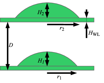
We consider a QDM formed by two self-assembled InAs dots in a GaAs matrix. The geometry of the structure as used in our modeling is shown in Fig. 1. The QDs are modeled as two spherical segments with base radii , and heights , , respectively. Throughout the paper, the aspect ratio of the two dots will be held constant, . Both dots are placed on a wetting layer with thickness . The dots are separated by a distance (base to base). A diffusion layer of a very small thickness nm is included at the contact between the two materials, in which the InAs concentration varies linearly. Apart from this, the InAs content is assumed to be 100% inside the dots and the wetting layers and 0 outside. The parameters of the modeled structure are collected in Table 1.
Our model includes the case of a single electron in the QDM as well as of two electrons coupled by the Coulomb interaction. The carriers interact with bulk acoustic phonons via standard deformation potential and piezoelectric interaction mechanisms.
The modeling proceeds in three steps: (1) Determination of the strain distribution; (2) Calculation of the wave functions for single- and two-electron states; (3) Calculation of relaxation rates. As each of these steps involves a specific formalism, the corresponding details of the model will be subsequently introduced in the following sections.
III Strain
In this section, we calculate the strain present in the inhomogeneous structure.
The strain fields in the system will be described by the strain tensor
where is the displacement field at the point in the crystal. The elastic energy of the inhomogeneous system is[44]
| (1) | |||||
Here are position-dependent elastic constants (see Table 1 for the values), in a QD and in GaAs, where and are the lattice constants of InAs and GaAs, respectively. The last term in Eq. (1) accounts for the mismatch of the lattice constants, shifting the equilibrium of the InAs crystal lattice to the state appropriately stretched with respect to the ideal InAs crystal. Since the strain is calculated with respect to the GaAs lattice and GaAs crystal coordinates are used, after minimizing the strain energy the results for the InAs dots must be rescaled to yield physical strain, according to[44]
| (2) |
For an axially symmetric structure, it is convenient to perform the computation in cylindrical coordinates . Therefore we denote the components of the displacement in the local reference frame as and define the corresponding components of the strain tensor,
We will look for the minimum of in the class of axially symmetric displacement fields, that is, and . With this assumption, the integration over in Eq. (1) can be performed analytically and one gets
| (3) | |||||
where and .

The displacement field minimizing is found by the conjugate gradient method on a square grid of 1000 points along and 666 point along , representing a cylinder with the height of nm and the radius of nm. The boundary conditions represent displacements due to the equilibrium strain in a system with two wetting layers, which corresponds to the actual situation at large distances from the dots. A combination of discretizations with forward and backward representations of derivatives is used to avoid discretization-induced oscillations [44]. As an example of the result, a strain map representing the hydrostatic and axial strain across the structure for a selected geometry is shown in Fig. 2.
IV Single electron states
In this section, we calculate approximate wave functions for a single electron confined in the nanostructure. This is done within a variational multi-component envelope function scheme [48] based on the fact that the confinement volume is large compared to the crystal lattice cell and that the local system parameters change relatively slowly on atomic scales. In this approach, one finds the values of effective masses and band edges at a given point by solving the bulk model with strain and composition equal to those present at a given point. This yields the band edge position, which is used as the local effective potential, as well as the band curvatures, which define the components of the effective mass tensor at a given point of the inhomogeneous heterostructure.
The conduction band structure in a strained system is determined from the 8-band (Kane) Hamiltonian with strain-induced terms (Bir-Pikus Hamiltonian) using the Löwdin elimination [49]. The part of the Hamiltonian coupling conduction and valence band states is [50]
where ’e‘ ’lh‘, ’hh‘, and ’so‘ denote the electron, heavy-hole, light-hole and spin-orbit split-off subbands, and represent the spin orientation in a given subband,
and
where is proportional to the interband momentum matrix element (see Table 1 for parameter values). The conduction band part of the Hamiltonian is
where is the free electron mass, is the conduction band edge in a bulk unstrained crystal, is the conduction band deformation potential, and is the hydrostatic strain.
As we are interested in the corrections to the conduction band energies up to and the off-diagonal elements and are proportional to we only need the conduction-valence band energy difference at . In this limit, the diagonal terms for the valence band states are
where is the valence band edge of an unstrained crystal, is the spin-orbit split-off parameter of an unstrained crystal, ,
and are valence band deformation potentials. The values of material parameters are given in Table 1.
Neglecting the strain-related terms in and , which are much smaller than the purely kinetic ones, we get the conduction band energy up to the 2nd order in ,
where the in-plane and components of the effective mass tensor are
and
where and , for . Note that are position dependent.


The dynamics of an electron in the strained nanostructure in the present approach is defined by the conduction band edge at a given point, (which depends on the local strain), and on the effective masses, which also vary across the structure. Fig. 3 shows an example of the profiles of the conduction band edge as a function of at three different values of . In Fig. 4, we show the spatial maps of the radial and axial components of the electron effective mass. Some strain-induced anisotropy of the effective mass can be seen. The value of the radial component, is close to the bulk GaAs value and much higher than the bulk InAs value of . It is roughly constant within the volumes of the two dots. The axial component is lower (about ) and shows some gradient along the QD axis, with higher values towards the top.
The envelope function of an electron is found from the Schrödinger equation with the Hamiltonian
Following the concept of ’adiabatic‘ separation of variables [51], we first numerically solve the one-dimensional equation along the strongest confinement direction at each ,
The lowest two solutions to this equation, , represent the lowest subband of confined states in the double well system. The corresponding two branches of -dependent eigenvalues, can be interpreted as effective potentials for the radial problem.
Next, we apply the Ritz variational method [52], looking for the stationary points of the functional
in the class of normalized ansatz functions
| (4) |
where is the angular momentum. Upon transforming to cylindrical coordinates and imposing the normalization via the Lagrange multiplier , we write the functional in the explicit form
We discretize the functional on the same lattice that was used in the computation of the strain. As the functional is quadratic, the stationarity requirement with respect to the values at the discrete points can easily be cast into the form of a matrix eigenvalue problem for the components . By virtue of the Ritz theorem [52], the corresponding eigenvalues , approximate the energy eigenvalues of the original problem, while the eigenvectors, representing the components at the discrete lattice points in the radial direction, are used to construct the electron eigenfunctions according to the ansatz formula (4). In this paper, the discussion will be restricted to the two lowest states for , corresponding to the tunnel-split ground state of the double-dot system.

The single particle eigenenergies found within our approach for three different distances between the dots are shown in Fig. 5(a-c). In these calculations, the shape of the lower dot is kept constant, while the base radius of the upper dot and its height are varied, with constant. Electronic (tunnel) coupling between the dots leads to the appearance of an anticrossing pattern near the point where the dots become equal. The width of the anticrossing is , where the phenomenological ’’tunnel coupling‘‘ is very well fitted by the formula , with nm-1 and eV. The value of is consistent with the one-dimensional semiclassical formula if one uses as found in the area between the dots (see Fig. 4), the potential barrier height meV (Fig. 3) and the electron energy meV (Fig. 5).
In accordance with the spectral anticrossing, the electron occupations for the ground and first excited states are transferred between the dots, as shown in Figs. 5(d-f). The exact resonance point, where the two occupations are equal to 1/2 for both states (corresponding to delocalized symmetric and antisymmetric wave functions), appears for slightly smaller than which results from the strain field in the absence of mirror symmetry in the structure.
The procedure proposed here, involving the variational problem for a two-component envelope, allows for mixing of the two manifolds of states related to the two functions and , which is essential when the two QDs are of similar size or when the thinner dot has a larger in-plane size, so that a crossing of the one-dimensional solutions appears at a certain value of .
V Coulomb interaction and two-electron states
We will find the two-electron states in the restricted basis of low-energy configurations of the two electron system. We discuss the situation when the energy difference between the ground states in the two dots is smaller than the intra-dot excitation energy (the latter is about 50 meV). Then the two lowest single-particle states found in Sec. IV correspond to an electron in the ground state of one of the dots or, near the resonance, to a delocalized superposition of the two ground states.
Let denote the annihilation and creation operators for an electron in the state with the wave function and spin . The low-energy two-electron configurations split into one triplet state (of no interest in the present discussion) and three singlet states
| (5a) | |||||
| (5b) | |||||
| (5c) | |||||
where is the vacuum (empty dot) state.
The Hamiltonian of the interacting two-electron system has the form
| (6) |
where
| (7) | |||||
Here is the electron charge, is the vacuum permittivity, and is the dielectric constant of the semiconductor. Some technical details concerning the calculation of Coulomb matrix elements for the wave functions obtained within the variational two-component envelope function scheme in Sec. IV are given in the Appendix.

In Fig. 6, we show the three lowest spin-singlet eigenstates of the interacting two-electron system as a function of the size of the upper dot with the lower dot kept fixed. The central resonance occurs when the dots are close to identical and involves the doubly occupied configurations and which, at the resonance point, have similar energy. This anticrossing is very narrow (less than meV for nm) since the two states involved differ by the location of both electrons [see Figs. 6(d)-(f)] and, therefore, are coupled only by very small exchange-like Coulomb terms. Only for the smallest inter-dot distance considered, nm, this splitting becomes larger due to stronger mixing of configurations and incomplete electron localization in the two states (which allows the configurations to be coupled by single-electron tunneling). The other two anticrossings occur at the degeneracy point between the singly occupied configuration (favored by the Coulomb repulsion) and the or configuration with two electrons in the larger dot. One can notice that these two splittings are wider than those appearing between the single-electron states, shown in Fig. 5 (for instance, 2 meV vs. 1.5 meV for nm). This is due to the fact that the anticrossing of two-electron configurations is enhanced by Coulomb terms [15].
VI Phonon-assisted relaxation
In this section, we discuss the phonon-assisted relaxation between the single-electron states and between the two lowest two-electron states.
The coupling between the electrons and phonons is described by the Hamiltonian
| (8) |
where the coupling constants have the symmetry . The inter-level energy distance in our structure is smaller than the optical phonon energy. Therefore, only acoustic phonons are relevant in our model. We include the deformation potential (DP) coupling to longitudinal acoustic (LA) phonons and the piezoelectric (PE) coupling to LA as well as transverse acoustic (TA) phonons. The coupling constant for the DP coupling mechanism is given by
| (9) |
where is the crystal density, is the normalization volume of the phonon modes, is the longitudinal speed of sound (see Table 1 for parameter values), and the form factor is defined as
| (10) |
The coupling element for PE interactions reads
| (11) |
where is the speed of sound (l,t denotes the LA and TA phonon branch, respectively) and is the piezoelectric constant. The function does not depend on the value of the phonon wave vector, but only on its orientation. For a zinc-blende structure, it reads
| (12) | |||||
where is the unit polarization vector for the phonon wave vector and polarization , and . We choose the following phonon polarization vectors
| (13) | |||||
for which the functions read
| (14) | |||||
In what follows, we will assume that higher states are separated by an energy much larger than , where is the Boltzmann constant and is the temperature. Then, the kinetics leading to thermalization of the occupations of the two relevant levels can be characterized by the occupation of the upper state,
where is the initial occupation, is the relaxation (thermalization) rate and
is the equilibrium occupation, where is the energy separation between the two states.
Thus, given the initial condition and the energy difference , the thermalization kinetics is determined by the relaxation rate (or the relaxation time ) which will be found in the following sections, first for a single-electron, then for the two-electron case.
VI.1 Single electron relaxation
For a single electron system, the thermalization rate can be found directly from Eq. (8) using the Fermi golden rule. The result can be written in the form
| (15) |
where
is the Bose distribution and the spectral density is given by
| (16) |
where is the total coupling for the branch , that is, and for . In fact, due to different parity of the DP and PE couplings (as functions of ) the two contributions do not interfere and the spectral density (hence, also the thermalization rate) can be split into the corresponding two parts and .
In order to find the thermalization rate, we calculate the form-factors defined in Eq. (10) using the single-electron wave functions found for the strained double dot structure in Sec. IV (see Appendix). From these, we find the coupling constants given by Eq. (9) and Eq. (11) and the corresponding spectral densities given by Eq. (16). The rate then follows from the Fermi golden rule formula, Eq. (15).


The single particle relaxation rates are shown in Figs. 7(a-c) as functions of the upper dot size for three values of the inter-dot spacing (for the same sample geometries as in Fig. 5) and at three different temperatures. These three plots show that both the magnitude and the size dependence of the relaxation rate is different in these three cases. The interpretation of this behavior can be based on the Fermi golden rule in the form of Eq. (15), where the essential role is played by the spectral density defined in Eq. (16) and plotted (for nm) in Fig. 8.
The overall magnitude of the spectral density depends on the spatial overlap between the wave functions corresponding to the states involved in the transition. It is, therefore, large at the resonance and becomes smaller as the system is shifted off the resonance point Fig. 8(a). Apart from this, the spectral density shows oscillations in its high-frequency tail which are due to the essentially one-dimensional emission of short wavelength phonons along the strongest confinement direction [53]. As we deal with two confinement centers displaced along the same direction, interference effects appear and the phonon emission amplitude has a maximum whenever for an integer . Moreover, the envelope of the spectral density decays at high frequencies since the short wave length phonons are not effectively coupled to the relatively weakly confined electron states.
In the case of closely stacked dots [Fig. 7(a)], the tunnel splitting of the QDM electron states is large and the frequency of the emitted phonons always lies far in the tail of the spectral density. This is reflected by the very low relaxation rate. The oscillations of the spectral density are clearly marked in the values of the relaxation rate. When the dots are separated by a larger distance [Fig. 7(b)], the resonance becomes narrower and now the resonant frequency lies in the region of large spectral density. When moving away from the resonance, the relaxation rate drops down primarily due to the decreasing overlap of the wave functions. This leads to a narrow peak in the dependence of the relaxation rate around the resonance value. Still, oscillations are visible in the slopes of this peak. For even larger inter-dot distances [Fig. 7(c)], the resonance becomes very narrow. Correspondingly, the overlap between the wave functions decays almost completely already when the size of the upper dot is changed by a fraction of a nanometer from the resonant value. Therefore, the relaxation rate is large only in a very narrow region around the resonance. The rates are also generally lower than in the previous case, which results from the dependence of the spectral density at low frequencies ( for the DP coupling and for the PE coupling).
The interplay between the shape and magnitude of the spectral densities for different coupling mechanisms [Fig. 8(b)] and the electron energies near the resonance is reflected also by the different contributions from the DP and PE couplings to the total relaxation rates. As can be seen in Figs. 7(d-f), the DP coupling dominates for large energy splittings. The reason is that this coupling is isotropic and involves LA phonons which have higher energies. On the contrary, the piezoelectric coupling is anisotropic and, according to Eq. (14), is suppressed for emission along the direction that is preferred at high frequencies. The situation changes at low energy splittings where the low-frequency properties of the spectral density are relevant. As the spectral density for the piezoelectric coupling decreases at more slowly than that corresponding to the DP coupling the PE coupling is the dominating mechanism in the case of narrow anticrossing, as can be seen in Fig. 7(f). For very low frequencies, all the contributions to the spectral density are small, hence the phonon-assisted relaxation process becomes ineffective for small energy splitting. This is manifested by a dip in the thermalization rate at the exact resonance for nm [Fig. 7(f)].

In Fig. 9 we show the energy splitting between the two lowest energy levels and the corresponding values of the thermalization rates as a function of the inter-dot distance for two system geometries: slightly different dots [Fig. 9(a,c)] and identical dots [Fig. 9(b,d)]. The values of the rates show oscillations, resulting from the variation of the energy level splitting and corresponding to the oscillations of the spectral density, as discussed above. The maximum value is quite large and corresponds to relaxation times of several picoseconds, which results from the relative proximity of the resonance (identical dots) in both presented cases. The maximum goes down and shifts to lower distances as the dots become different. At large distances the relaxation becomes inefficient in any case. In an attempt (not shown) to compare the decrease of the rates at large with an exponential law (as observed, at least approximately, in some experiments [22, 26, 24, 23]), we have found a roughly exponential decay with a coefficient consistent with the value of found in Sec. IV. This decay is, however, strongly modulated by oscillations. This results from a small energy scales in our model which is comparable to strain-related effects as the dots are moved with respect to each other. This is visible in Figs. 9(a,c), where the energy level separation does not tend to a constant asymptotic value at large as would be expected for a simple model of two potential wells with fixed shapes.
VI.2 Relaxation in two-electron systems
In this section, we calculate the transition rates for phonon-assisted relaxation between two-electron states , obtained from the diagonalization of the Hamiltonian (6) in the restricted basis formed by the states and [Eqs. (5a)-(c)]. We first project the carrier-phonon Hamiltonian (8) onto the two-electron subspace,
where the coupling constants
are found based on the numerical results for the states . We restrict the discussion to transitions between the two lowest states and , separated by an energy splitting . In the Fermi golden rule approximation, the rate for the relaxation of the two occupations to equilibrium is
where the spectral density is given by

The inverse relaxation times resulting from these calculations are presented in Fig. 10. Like in the single electron case, the energy level splitting in the case of relatively closely spaced dots ( nm) is very large and the resonance is very broad which results in very long relaxation times which do not vary considerably over the parameter range studied [Fig. 10(a)]. For such high transition energies, only LA phonons contribute to the process via DP coupling [Fig. 10(d)]. At larger inter-dot distances, the transition rates become large around the resonance points corresponding to the anticrossing of and or configurations. The structure of the relaxation rate as a function of the upper dot diameter is similar to that discussed in the single electron case above. Also the relative contributions form different coupling mechanisms behave in the same way, with the piezoelectric coupling dominating at low energies. In general, the relaxation rates are similar to those found in the single electron case, since both these processes are physically very similar. In both cases, the electron tunnels between the dots and simultaneously emits one phonon. The only difference is that in the single electron case it tunnels towards an empty QD, whereas in the two electron case, there is already another electron. This basically leads to shifts (due to Coulomb interaction) of the parameter regimes where the relaxation is most efficient from the region of identical dots to the asymmetric situation where the difference of confinement energies compensates for the Coulomb repulsion. A similar conclusion has been reached in the case of gated QDM structures modeled by Gaussian potential wells [15].
VII Conclusion
We have studied phonon-assisted relaxation (thermalization) for single-electron and two-electron configurations in self-assembled quantum dots. In order to describe the electron states in a strained structure in a possibly realistic (but still relatively simple) way and to reliably model the effect of the system geometry we have developed a generalized, multi-component envelope function formalism based on the variational principle.
Our results show that the single phonon relaxation is very efficient in an extremely narrow range of relative QD sizes near the anticrossings of energy levels but only for systems with a sufficiently large inter-dot distance (several nm). In this case, the relaxation times can be as low as 1 ps, both in the single-electron and two-electron cases. The range of efficient relaxation becomes narrower as the dots are more distant from each other. Both coupling channels, piezoelectric and deformation potential, are important for the overall relaxation rate. The former dominates at low (sub-meV) transition energies.
When the distance between the dots becomes smaller than about 10 nm, the energy level splitting becomes too large to be spanned by a single acoustic phonon (but still to small for an optical one). In this range of closely stacked dots, the tunneling times increase by orders of magnitudes and take values in the nanosecond range. For such small inter-dot distances, the energy splitting between the two lowest states is dominated by tunnel coupling and depends weakly on the size difference. As a result, the efficiency of the relaxation process remains nearly constant over a wide range of dot sizes. One can expect, however, that two-phonon processes [54] can be important in this range of parameters, in particular for energy splittings exceeding the optical phonon energy. In general, decoherence in such systems may be dominated by pure dephasing due to occupation-conserving phonon scattering [55].
Our findings seem to be consistent with the general features of experimental observations. The size range where the relaxation is very efficient (on picosecond time scales) is extremely narrow and does not exceed a few Angstrom, which is comparable to the lattice constant of GaAs. This means that such an efficient relaxation between the two lowest states in self-assembled quantum dot molecules is a rather rare phenomenon which occurs only for very finely tuned (accidentally or intentionally) dots and is unlikely to be observed in a typical sample. Therefore, we conclude that relaxation times on the order of at least hundreds of picoseconds should be typical. The coupling between the dots decreases exponentially with the distance between them which reduces the overlap between the wave functions. Therefore, phonon-assisted tunneling for a spontaneously formed pair of non-identical dots should become inefficient as the spatial separation between between the dots grows beyond a certain distance, as is indeed observed in experiments [22, 26, 24, 23]. In the case studied here, that is, single-phonon relaxation between states separated by a few meV in energy, the relaxation rates undergo oscillations as functions of the geometrical parameters due to a structured nature of the phonon reservoir and the resulting interference effects. One should note, however, that most of the available experimental data correspond to systems which much larger energy splittings.
A more quantitative comparison is possible in the case of the measurements presented in Ref. 28. Here, electron tunneling (that is, a transition between spatially direct and indirect exciton states) has been studied for a QDM with a fixed 10 nm spacing and energy level difference of a few meV, which corresponds more closely to the physical situation of our model. Our calculations for such parameter range yield transfer times in the range of hundreds of picoseconds, which reasonably agrees with the measured time of 0.5 ns (note that a slightly different material system was used in that experiment and that some details of the system geometry are not exactly known). It will be interested to include the electric field in our model and to seek a closer correspondence with the experiment, which is planned as a future work.
Acknowledgements.
This work was partly supported by Grant No. N N202 1336 33 of the Polish MNiSW.Appendix A Form factors and Coulomb matrix elements
In this appendix, we briefly summarize the method of calculating the form factors and Coulomb matrix elements based on the wave functions obtained within the variational multi-component envelope function formalism using the simplification offered by a cylindrically symmetric system.
Using the identity
one writes the Coulomb matrix element given by Eq. (7) in the form
| (17) |
where the form factors are given by Eq. (10).
We will use cylindrical coordinates for the vector and spherical coordinates for the vector , where and . For wave functions in the form given in Eq. (4), one has
| (18) |
where
| (19) | |||||
In Eqs. (18) and (19), we denoted the angular momenta of the two states by , used the identity
where is the -th Bessel function, and introduced the quantities
which are calculated by fast Fourier transform on the grid.
References
- [1] G. W. Bryant, Phys. Rev. B 47, 1683 (1993).
- [2] A. Schliwa, O. Stier, R. Heitz, M. Grundmann, and D. Bimberg, Phys. Stat. Sol. (b) 224, 405 (2001).
- [3] B. Szafran, S. Bednarek, and J. Adamowski, Phys. Rev. B 64, 125301 (2001).
- [4] G. Bester, J. Shumway, and A. Zunger, Phys. Rev. Lett. 93, 047401 (2004).
- [5] G. Ortner, I. Yugova, G. Baldassarri Höger von Högersthal, A. Larionov, H. Kurtze, D. R. Yakovlev, M. Bayer, S. Fafard, Z. Wasilewski, P. Hawrylak, Y. B. Lyanda-Geller, T. L. Reinecke, A. Babinski, M. Potemski, V. B. Timofeev, and A. Forchel, Phys. Rev. B 71, 125335 (2005).
- [6] M. Bayer, P. Hawrylak, K. Hinzer, S. Fafard, M. Korkusinski, Z. R. Wasilewski, O. Stern, and A. Forchel, Science 291, 451 (2001).
- [7] G. Ortner, M. Bayer, A. Larionov, V. B. Timofeev, A. Forchel, Y. B. Lyanda-Geller, T. L. Reinecke, P. Hawrylak, S. Fafard, and Z. Wasilewski, Phys. Rev. Lett. 90, 086404 (2003).
- [8] G. Ortner, M. Bayer, Y. Lyanda-Geller, T. L. Reinecke, A. Kress, J. P. Reithmaier, and A. Forchel, Phys. Rev. Lett. 94, 157401 (2005).
- [9] H. J. Krenner, M. Sabathil, E. C. Clark, A. Kress, D. Schuh, M. Bichler, G. Abstreiter, and J. J. Finley, Phys. Rev. Lett. 94, 057402 (2005).
- [10] Z. J. Wu, K. D. Zhu, X. Z. Yuan, Y. W. Jiang, and H. Zheng, Phys. Rev. B 71, 205323 (2005).
- [11] V. López-Richard, S. S. Oliveira, and G.-Q. Hai, Phys. Rev. B 71, 075329 (2005).
- [12] V. N. Stavrou and X. Hu, Phys. Rev. B 72, 075362 (2005).
- [13] S. Vorojtsov, E. R. Mucciolo, and H. U. Baranger, Phys. Rev. B 71, 205322 (2005).
- [14] J. I. Climente, A. Bertoni, G. Goldoni, and E. Molinari, Phys. Rev. B 74, 035313 (2006).
- [15] A. Grodecka, P. Machnikowski, and J. Förstner, Phys. Rev. B 78, 085302 (2008).
- [16] A. Grodecka-Grad and J. Förstner, Phys. Rev. B 81, 115305 (2010).
- [17] K. Roszak and P. Machnikowski, Phys. Rev. B 80, 195315 (2009).
- [18] T. Kazimierczuk, J. Suffczyński, A. Golnik, J. A. Gaj, P. Kossacki, and P. Wojnar, Phys. Rev. B 79, 153301 (2009).
- [19] M. Goryca, T. Kazimierczuk, M. Nawrocki, A. Golnik, J. A. Gaj, P. Kossacki, P. Wojnar, and G. Karczewski, Phys. Rev. Lett. 103, 087401 (2009).
- [20] S. D. Barrett and T. M. Stace, Phys. Rev. B 73, 075324 (2006).
- [21] S. Rodt, V. Turck, R. Heitz, F. Guffarth, R. Engelhardt, U. W. Pohl, M. Straßburg, M. Dworzak, A. Hoffmann, and D. Bimberg, Phys. Rev. B 67, 235327 (2003).
- [22] R. Heitz, I. Mukhametzhanov, P. Chen, and A. Madhukar, Phys. Rev. B 58, R10151 (1998).
- [23] M. Reischle, G. J. Beirne, R. Roßbach, M. Jetter, H. Schweizer, and P. Michler, Phys. Rev. B 76, 085338 (2007).
- [24] Y. I. Mazur, Z. M. Wang, G. G. Tarasov, M. Xiao, G. J. Salamo, J. W. Tomm, V. Talalaev, and H. Kissel, Appl. Phys. Lett. 86, 063102 (2005).
- [25] J. Seufert, M. Obert, G. Bacher, A. Forchel, T. Passow, K. Leonardi, and D. Hommel, Phys. Rev. B 64, R121303 (2001).
- [26] A. Tackeuchi, T. Kuroda, K. Mase, Y. Nakata, and N. Yokoyama, Phys. Rev. B 62, 1568 (2000).
- [27] W.-H. Chang, H. Lin, S.-Y. Wang, C.-H. Lin, S.-J. Cheng, M.-C. Lee, W.-Y. Chen, T.-M. Hsu, T.-P. Hsieh, and J.-I. Chyi, Phys. Rev. B 77, 245314 (2008).
- [28] T. Nakaoka, E. C. Clark, H. J. Krenner, M. Sabathil, M. Bichler, Y. Arakawa, G. Abstreiter, and J. J. Finley, Phys. Rev. B 74, 121305(R) (2006).
- [29] G. Ortner, R. Oulton, H. Kurtze, M. Schwab, D. R. Yakovlev, M. Bayer, S. Fafard, Z. Wasilewski, and P. Hawrylak, Phys. Rev. B 72, 165353 (2005).
- [30] F. V. de Sales, S. W. da Silva, J. M. R. Cruz, A. F. G. Monte, M. A. G. Soler, P. C. Morais, M. J. da Silva, and A. A. Quivy, Phys. Rev. B 70, 235318 (2004).
- [31] B. D. Gerardot, S. Strauf, M. J. A. de Dood, A. M. Bychkov, A. Badolato, K. Hennessy, E. L. Hu, D. Bouwmeester, and P. M. Petroff, Phys. Rev. Lett. 95, 137403 (2005).
- [32] K. Nishibayashi, T. Kawazoe, M. Ohtsu, K. Akahane, and N. Yamamoto, Appl. Phys. Lett. 93, 042101 (2008).
- [33] J. H. Park, D. G. Choi, T. K. Lee, E. Oh, S. Lee, and J. K. Furdyna, Appl. Phys. Lett. 90, 201916 (2007).
- [34] P. Bajracharya, T. A. Nguyen, S. Mackowski, L. M. Smith, H. P. Wagner, U. W. Pohl, D. Bimberg, and M. Strassburg, Phys. Rev. B 75, 035321 (2007).
- [35] T. Nakaoka, J. Tatebayashi, Y. Arakawa, and T. Saito, J. Appl. Phys. 96, 150 (2004).
- [36] B. R. Wang, B. Q. Sun, Y. Ji, X. M. Dou, Z. Y. Xu, Z. M. Wang, and G. J. Salamo, J. Appl. Phys. 93, 011107 (2008).
- [37] A. O. Govorov, Phys. Rev. B 68, 075315 (2003).
- [38] A. O. Govorov, Phys. Rev. B 71, 155323 (2005).
- [39] M. Richter, K. J. Ahn, A. Knorr, A. Schliwa, D. Bimberg, M. E.-A. Madjet, and T. Renger, Phys. Stat. Sol. (b) 243, 2302 (2006).
- [40] E. Rozbicki and P. Machnikowski, Phys. Rev. Lett. 100, 027401 (2008).
- [41] Q. Xie, A. Madhukar, P. Chen, and N. P. Kobayashi, Phys. Rev. Lett. 75, 2542 (1995).
- [42] G. S. Solomon, J. A. Trezza, A. F. Marshall, and J. S. Harris, Jr., Phys. Rev. Lett. 76, 952 (1996).
- [43] C. Pryor, Phys. Rev. B 57, 7190 (1998).
- [44] C. Pryor, J. Kim, L. W. Wang, A. J. Williamson, and A. Zunger, J. Appl. Phys. 83, 2548 (1998).
- [45] M. Korkusiński and P. Hawrylak, Phys. Rev. B 63, 195311 (2001).
- [46] J. Andrzejewski, G. Sęk, E. O‘Reilly, A. Fiore, and J. Misiewicz, J. Appl. Phys. 107, 073509 (2010).
- [47] D. Obreschkow, F. Michelini, S. Dalessi, E. Kapon, and M.-A. Dupertuis, Phys. Rev. B 76, 035329 (2007).
- [48] M. Pochwała and P. Machnikowski, Acta Phys. Polon. A 114, 1285 (2008).
- [49] P. O. Löwdin, J. Chem. Phys. 19, 1396 (1951).
- [50] T. B. Bahder, Phys. Rev. B 41, 11992 (1990).
- [51] A. Wójs, P. Hawrylak, S. Fafard, and L. Jacak, Phys. Rev. B 54, 5604 (1996).
- [52] A. Messiah, Quantum Mechanics (North-Holland, Amsterdam, 1966).
- [53] U. Bockelmann and G. Bastard, Phys. Rev. B 42, 8947 (1990).
- [54] V. N. Stavrou and X. Hu, Phys. Rev. B 73, 205313 (2006).
- [55] P. Machnikowski, Phys. Rev. Lett. 96, 140405 (2006).