In-Plane Magnetoresistance on the Surface of Topological Insulator
Abstract
We study the tunneling magneto-transport properties of the Ferromagnetic Insulator-Normal Insulator-Ferromagnetic Insulator(FNF) and Ferromagnetic Insulator-Barrier Insulator-Ferromagnetic Insulator (FBF) junctions on the surface of topological insulator in which in-plane magnetization directions of both ferromagnetic sides can be parallel and antiparallel. We derive analytical expressions for electronic conductances of the two mentioned junctions with both parallel and antiparallel directions of magnetization and using them calculate magnetoresistance of the two junctions. We use thin barrier approximation for investigating the FBF junction. We find that although magnetoresistance of the FNF and FBF junctions are tunable by changing the strength of magnetization texture, they show different behaviors with variation of magnetization. In contrast to the magnetoresistance of FNF, magnetoresistance of FBF junctions shows very smooth enhance by increasing the strength of magnetization. We suggest an experimental set up to detect our predicted effects.
Keywords:
Topological Insulator, In-plane Magnetoresistance, Electronic Conductance, magneto-transportPACS
74.78.Na, 71.10.Pm, 72.25.Dc, 85.75.-d1 Introduction
Recently, some topological insulators (TI) are observed experimentally and investigated theoretically [1, 2, 3, 4, 5, 6, 7, 8, 9, 13, 14, 11, 12]. A TI is an insulator in bulk but a robust conducting in edge even in presence of deformation or strong disorder i.e. it is gapless only in surface. So it can carry charge current on its surface even in the absence of magnetic field. This state of condensed matter is due to spin-orbit coupling and protected by origin of time-reversal symmetry [8, 9, 5]. For two-dimensional TI we have helical modes (the spin orientation of surface electrons are perpendicular to momentum direction ) at the edges [2], similar to quantum Hall systems.
This property is reason for some interesting physical properties of the system[10]. For three-dimensional TI, strong (weak) TI is defined for odd (even) number of chiral Dirac fermions on surface[9]. In graphene, There are four Dirac cones in momentum space [15], but the number of Dirac cones in TI’s edge are odd. So there are good unconventional properties such as fractional quantum Hall effect, Berry’s phases and immunity to Anderson localization due to odd spin-Dirac on the surface[1, 6, 16, 17]. On the other hand, studying of transport properties is useful to understand the macroscopic and applicatory properties. Some attractive physical properties are seen when TI is on proximity of ferromagnet or superconductor[18, 19, 20, 13, 14]. Also the tunneling magnetoresistance (TMR) effect has attracted much interest because of crucial applications in spintronics [21]. In this paper we investigate TMR and transport properties of the Dirac fermions on the surface of topological insulator for FNF and FBF junctions within the clean limit and low temperature regime. We assume that the used topological insulator is made of or . The advantage of the mentioned alloys is their single Dirac cone in Berillouin zone in which two dimensional Dirac equation govern the Dirac fermions on surface of the topological insulator[1, 2, 6]. Due to the exchange coupling, the ferromagnetism can be induced on the surface of topological insulator when a ferromagnetic layer is deposited on top of it[24]. We use two dimensional Dirac Hamiltonian and derive wave functions in all regions. Using boundary conditions we obtain analytical expressions for reflection and transmission probabilities. Using the obtained reflection and transmission probabilities, we calculate electronic conductance of the two mentioned systems when the magnetization of ferromagnetic layers are parallel and antiparallel. To investigate properties of FBF junctions we use the thin barrier approximation. The used barrier can be made by applying a transverse voltage or doping[22, 23]. The main concern is to investigate the magnetoresistance of the mentioned systems and their differences.
2 Tunneling Magnetoresistance in FNF Junctions
On the surface of topological insulator Dirac fermions are governed by two dimensional Dirac Hamiltonian that is given by:
| (1) |
where is vector of Pauli matrices in spin space and I is identity matrix. Also, is Fermi velocity and is chemical potential. When a ferromagnetic electrode with magnetization m is deposited on surface of the TI, due to the proximity of TI and ferromagnetism, an additional term appear into Eq.(1) as follow[24]:
| (2) |
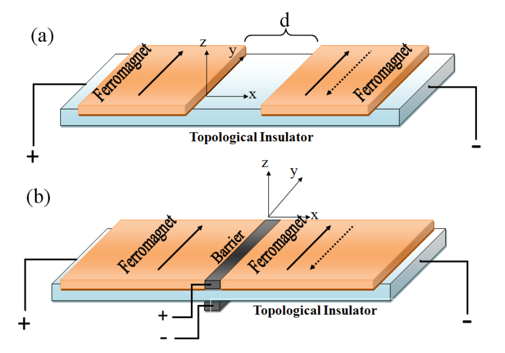
We consider an FNF junction in which thickness of normal region is . We assume the TI is located in -plane and two ferromagnetic electrodes is deposited on TI such that in which +(–) refers to parallel (antiparallel) in magnetization alignment of electrodes (See Fig. 1). Here is the well known step function. By solving the Eq. (1) for region, Dirac spinors read as:
| (3) |
where and are components of wave vector in and directions, respectively. Also the sings refer to the directions of the -axis and is incidental angle of the Dirac fermions which and are described as:
| (4) |
where depends on the exchange coupling and one can tune the parameter via an external field[24]. For normal region between , Dirac spinors are given by:
| (5) |
in which is -component of the wave vector and is angle of incidental Dirac fermions and are defined as:
| (6) |
In region , there are two choices, parallel or antiparallel directions for magnetization of the electrodes. When we make our system with parallel magnetization, all spinors are similar to Eq. (3) but for antiparallel case the spinors read:
| (7) |
in which and are defined as:
| (8) |
As seen in Eqs.(4, 8), for antiparallel magnetization case when is larger than its critical value namely , the wave function in Eq. (7) decays. For an incidental particle from into the FN interface at , the transverse wave vector and excitation energy are conserved in scattering process. The Dirac spinors within each region must satisfy the following boundary conditions at :
| (9) |
and at :
| (10) |
By solving Eqs.9 and 10, transmission probability for parallel and antiparallel magnetization directions are derived as:
| (11) |
| (12) |
where and . The P and AP indexes stand for parallel and antiparallel magnetizations. The Eqs.11 and 12 are the main results of this section. Using the transmission probabilities and conductance formula[23], one can calculate the conductances of the mentioned structures containing parallel and antiparallel magnetizations,
| (13) |
here is normal conductance
and is
density of state of Dirac fermions and is width of the junction.
The conductances of the parallel and antiparallel magnetization
are plotted versus in Fig.2, here
is Fermi vector of the system. The oscillatory
behavior of both conductances are results of coherent interference
of the Dirac fermions at two interfaces. By using the conductances
of parallel and antiparallel magnetization, one can calculate the
magnetoresistance of the system which is defined as . This quantity may have many interesting
and important applications in spintronic industry, in similarity
with the Ref. [21]. The plotted magnetoresistance as a
function of is shown in Fig.3 which shows
oscillatory behavior for all of the gate voltages as we expected.
This oscillatory behavior is a result of oscillatory behavior in
conductances for parallel and antiparallel magnetizations. The
plotted magnetoresistance as a function of can be seen in
Fig.4 that is also one of the main results of this
section. By increasing , the magnetoresistance enhance to reach
the perfect value in . Although for small values of the
magnetoresistance oscillates, the quantity for large values of
, shows a smooth behavior. Now we proceed to present an
investigation of the FI/BI/FI junction.
3 Tunneling Magnetoresistance in FBF Junctions
Now we focus our attention to FBF junctions. For producing such structures one can apply a transverse gate voltage into the normal region and make it as a barrier for moving Dirac fermions from left ferromagnet electrode to interface (See Fig.1, part (b)). By applying the barrier voltage, another additional term added to the Dirac Hamiltonian Eq. (1) for normal region and change it as:
| (14) |
Dirac fermion states within the barrier region are:
| (15) |
where and are defined as:
| (16) |
We are interested in the influence of thin barrier regime on the magnetoresistance. In this limit, width of the junction approaches to zero and barrier voltage move to large values simultaneously so that the barrier strength remains constant. In this limit and . Substituting the present Dirac spinors Eq. (15) into the boundary conditions Eqs.9 and 10 , we have derived the transmission probabilities for parallel (P label) and antiparallel (AP label) structures within the thin barrier regime as below:
| (17) | |||||
| (18) |
where and . The above obtained analytical expressions for the transition probabilities of parallel and antiparallel structures are other results of the present paper. As seen in Eq. (18), for an incidental particle with normal direction to the interface, the transmission probability is equal to unity. This situation is similar to the Klein tunneling in quantum relativistic theory [25]. To calculate the conductance of the mentioned parallel and antiparallel structure within the thin barrier regime, one should use the obtained transmission probabilities (Eqs.17,18) in Eq. (13). The plotted conductances for both parallel and antiparallel magnetization are shown in Fig.5 as a function of the barrier strength . Changing the gate voltage doesn’t make any changes in the positions of the extremum in conductances of parallel and antiparallel magnetization. The maximum of parallel conductance has phase difference with respect to antiparallel case. Unlike damping oscillatory behavior of MR versus length of the normal region in FNF case (See Fig.3), here the oscillatory behavior of the conductance leads to harmonic oscillations in MR, as shown in Fig.6. We plotted the magnetoresistance for this set up as a function of , as shown in Fig.7, which approximately shows linear behavior. This linear manner in magnetoresistance for FBF junction seems to be more applicatory than the discussed behavior of magnetoresistance in FNF junctions. By tuning the gate voltage and exchange coupling due to the ferromagnetic electrodes, we can access to an arbitrary value in magnetoresistance which is useful in spintronics.
4 Conclusions
In summary, we have investigated the electronic transport properties of topological insulator-based ferromagnetic/normal/ferromagnetic (FNF) and topological insulator-based ferromagnetic/barrier/ferromagnetic FBF junctions on the surface of topological insulator in low temperature and clean regimes. We assumed the two magnetizations are in-plane and deposited on the surface of topological insulator. We have derived analytical expressions for transmission probabilities of two different magnetization directions, parallel and antiparallel for FNF and FBF junctions. To investigate electronic properties of the FBF junction, in our calculations we assumed that and simultaneously. This approximation is well known as thin barrier approximation. Using the derived transition probabilities, conductances and magnetoresistances of the systems were calculated. We have found that the very important quantity of such junctions (magnetoresistance) shows different behavior by increasing the magnetization strength of ferromagnetic region for FNF and FBF junctions. Although magnetoresistance of the two junctions can be tuned from values near up to , magnetoresistance for FNF junctions shows oscillatory behavior vs. the magnetization strength, variation of the quantity vs. for FBF junctions behave like a very smooth enhancement.
5 Acknowledgments
The authors appreciate very useful and fruitful discussions with Jacob Linder. Rasoul Ghasemi also is appreciated for helpful points in revision. We would like to thank the Office of Graduate Studies of Isfahan University.
References
- [1] D. Hsieh et al., Nature (London) 460, 1101 (2009);
- [2] B. A. Bernevig, T. L. Hughes, and S.-C. Zhang, Science 314, 1757 (2006); B. A. Bernevig and S. C. Zhang, Phys. Rev. Lett. 96, 106802 (2006).
- [3] M. Koenig et al., Science 318, 766 (2007); D. Hsieh et al., Nature (London) 452, 970 (2008).
- [4] C. L. Kane and E. J. Mele, Phys. Rev. Lett. 95, 226801 (2005).
- [5] J. E. Moore et al., Phys. Rev. B 75, 121306(R) (2007).
- [6] Y. Xia et al. Nature Phys. 5, 398 (2009).
- [7] Y. S. Hor et al. Phys. Rev. B 79, 195208 (2009).
- [8] L. Fu et al., Phys. Rev. Lett. 98, 106803 (2007).
- [9] L. Fu and C. L. Kane, Phys. Rev. B 76, 045302 (2007).
- [10] L. Fu and C. L. Kane, Phys. Rev. Lett. 100, 096407 (2008).
- [11] H. Zhang, C. Liu, X. Qi, X. Dai, Z. Fang and S. Zhang, Nat. Phys 5, 438 (2009).
- [12] S. Raghu, S. Chung, X. Qi, and S. Zhang, Phys. Rev. Lett. 104, 116401 (2010)
- [13] J. Linder, Y. Tanaka, T. Yokoyama, A. Sudbø and N. Nagaosa, Phys. Rev. Lett. 104, 067001 (2010).
- [14] J. Linder, Y. Tanaka, T. Yokoyama, A. Sudbø and N. Nagaosa, Phys. Rev. B 81, 184525 (2010).
- [15] K. S. Novoselov et al. Nature (London) 438, 197 (2005).
- [16] X. L. Qi, T. L. Hughes and S.-C. Zhang. Phys. Rev. B 78, 195424 (2008).
- [17] A. P. Schnyder, S. Ryu, A. Furusaki and A. W. W. Ludwig. Phys. Rev. B 78 195125 (2008).
- [18] A. Essin, J. E. Moore and D. Vanderbilt. Phys. Rev. Lett. 102, 146805 (2009).
- [19] M. Franz. Physics 1, 36 (2008).
- [20] A. R. Akhmerov, J. Nilsson and C. W. J. Beenakker. Phys. Rev. Lett. 102, 216404 (2009).
- [21] I. Zutic, J. Fabian, and S. D. Sarma Rev. Mod. Phys. 76, 323 (2004).
- [22] Y. Tanaka, T. Yokoyama, and N. Nagaosa, Phys. Rev. Lett. 103, 107002 (2009).
- [23] S. Mondal, D. Sen, K. Sengupta, and R. Shankar, Phys. Rev. Lett. 104, 046403 (2010).
- [24] T. Yokoyama, Y. Tanaka, N. Nagaosa, arXiv:0907.2810v2.
- [25] O. Klein, Z. Phys. 53, 157 (1929).