Electronic transport through bilayer graphene flakes
Abstract
We investigate the electronic transport properties of a bilayer graphene flake contacted by two monolayer nanoribbons. Such a finite-size bilayer flake can be built by overlapping two semi-infinite ribbons or by depositing a monolayer flake onto an infinite nanoribbon. These two structures have a complementary behavior, that we study and analyze by means of a tight-binding method and a continuum Dirac model. We have found that for certain energy ranges and geometries, the conductance of these systems oscillates markedly between zero and the maximum value of the conductance, allowing for the design of electromechanical switches. Our understanding of the electronic transmission through bilayer flakes may provide a way to measure the interlayer hopping in bilayer graphene.
Keywords:
Graphene nanoribbons \sepElectronic properties \sepTransport properties \sepHeterostructurespacs
73.22.Pr, 73.23.AdI Introduction
Graphene is a sheet of carbon atoms that order in a honeycomb structure, which is composed of two inequivalent triangular sublattices and . Since its experimental isolation in 2004 [1] and the subsequent verification of its exotic properties, the interest in this material has boosted. Carriers in monolayer graphene behave as two-dimensional (2D) massless Dirac fermions, [2] with a linear dispersion relation . Phenomena of fundamental nature, such as quantum Hall effect [3, 4] and Klein [5, 6] tunneling have been recently measured in graphene based devices.
Being a material of atomic thickness, graphene is regarded as a promising candidate for nanoelectronic applications. [2] By patterning graphene, its electronic structure can be altered in a dramatic fashion: size quantization yields ribbons with electronic gaps, essential for electronics. [7, 8, 9] By imposing appropriate boundary conditions, the physics of graphene nanoribbons is well described within a continuum Dirac model. [10, 11, 12] Furthermore, connections and devices can be designed in a planar geometry by cutting graphene layers. [13] Another way to modify the band structure of graphene is to stack two graphene monolayers, and , forming a bilayer graphene. [14, 15, 16] In bilayer graphene there are four atoms per unit cell, with inequivalent sites , and , in the first and second graphene layers, respectively.
Different stacking orders can occur in bilayer graphene. Due to its larger stability for bulk graphite, the most commonly studied is (Bernal) stacking. In the stacking, the two graphene layers are arranged in such a way that the sublattice is exactly on top of the sublattice . In the simple hexagonal or stacking, both sublattices of sheet , and , are located directly on top of the two sublattices and of sheet . Although graphite with direct or stacking has not been observed in natural graphite, it has been produced by folding graphite layers at the edges of a cleaved sample with a scanning tunneling microscope tip; [17] additionally, the growth of -stacked graphite on (111) diamond has also been reported. [18] Furthermore, it has been recently found that stacking is surprisingly frequent in bilayer graphene, [19] so it should be also considered as a realistic possibility in few-layer graphene. The interplanar spacing for the stacking has been experimentally determined to be Å, [20], whereas for the stacking seems to be somewhat larger, Å. [18] First-principles calculations agree with these values. [21, 22, 23] In any case, the distance between atoms belonging to different layers in both stackings is much larger that the separation between atoms in the same layer, Å.
Nanostructures based on bilayer graphene have begun to be explored only recently. [24, 25, 16, 26, Fiori_2009a, Fiori_2009b] Bilayer graphene nanoribbons might present better signal-to-noise ratio in transport experiments than monolayer ribbons. [27] Graphene flakes are quantum-dot-like structures, and because of their aspect ratio they are also called nanobars. Both, bilayer nanoribbons and bilayer flakes, show interesting properties with an intriguing dependence on stacking. The dependence of the energy gap of bilayer graphene flakes on their width and length as well as on their atomic termination has been recently reported. [28]
In this paper we concentrate in the transport properties of bilayer armchair graphene flakes with nanoribbon contacts. We consider that the most likely way of achieving such quasi-zero dimensional structures is either by the overlap of two nanoribbons, depicted in the lower part of Fig. 1, or the deposition of a finite-size graphene flake over a graphene nanoribbon, shown in the upper part of Fig. 1. These two configurations correspond to two different ways of providing monolayer nanoribbon leads for the bilayer flake: either the ribbon leads are contacted to different layers of the flake, or to the same monolayer. We will address these two configurations as bottom-bottom () or bottom-top (), respectively. In both geometries the width of the bilayer flake and nanoribbons is the same, , and the length of the bilayer region is . In this work we consider narrow armchair metallic graphene nanoribbons in the energy range for which only one incident electronic channel is active.

We calculate the conductance with two different approaches: a tight-binding model using the Landauer-Büttiker formalism and a mode-matching calculation in the continuum Dirac-like Hamiltonian approximation. Our main results are the following:
i) In the stacking configuration, the transmission through the system shows antiresonances due to the interference of the two propagating electronic channels in the bilayer flake. For a bilayer region of length we obtain that the conductance oscillates as function of energy with a main period . For a fixed incident energy , the conductance as a function of the length oscillates with two main periods: and , being the interlayer hopping parameter. The bonding/antibonding character of the bilayer bands in the stacking makes the bottom-top and bottom-bottom conductances to be rather complementary: the conductance is zero in the bottom-top configuration and it is finite in the bottom-bottom arrangement at zero energy, and in general the maxima of the bottom-top configuration coincide with the minima of the bottom-bottom one and viceversa.
ii) For the stacking, and for energies larger than the interplane hopping , these devices behave similar to those in the configuration because there are also two propagating electron channels in the bilayer flake at these energies. The conductance presents antiresonances with periods depending on , , and . An interesting difference is that for a fixed incident energy, the period related with interlayer hopping is twice than that found for the stacking. This reflects that in the stacking only half of the atoms are connected by interlayer hopping, whereas in the arrangement all atoms are connected.
iii) For energies smaller than the interplane hopping, for which the stacking has only a propagating channel, the conductance shows Fabry-Perot-like resonances. These are associated with constructive interferences in the only available electronic channel. At zero energy the conductance of the bottom-bottom configuration is unity, whereas in the bottom-top geometry the conductance is zero.
We have analyzed the dependence of the transmission with the structural parameters and the interlayer coupling in bilayer graphene. This study provides a way to determine the interlayer hopping by studying the variation of the low energy conductance of two overlapping nanoribbons with the bilayer flake length; in addition, it could clarify the role of stacking in the transport characteristics of these systems. Our results also indicate that the conductance, as function of energy and system size, oscillates markedly between zero and a finite value, allowing for the design of electromechanical switches based on overlapping nanoribbons. The introduction of an external gate voltage is of interest for potential applications, however, we restrict ourselves to zero gate voltage in order to obtain analytical expressions in the Dirac model and acquire a physical understanding of the transport properties of these structures.
This work is organized as follows. In Section II we introduce the tight-binding and Dirac Hamiltonians we use to model the electronic properties of graphene. Section III is dedicated to describe the conductance calculations, both in the tight-binding approximation, for which we use Landauer-Büttiker formalism, and in the continuum Dirac-like model, where we use a wavefunction matching technique. Section IV is dedicated to present numerical results obtained in the tight-binding Hamiltonian and compare them with the analytical results obtained in the Dirac formalism. Finally, we conclude in Section V summarizing our main results.
II Theoretical description of the system
The low energy properties in graphene are mainly determined by the orbitals. Thus, we adopt a -band tight-binding Hamiltonian with nearest-neighbor in-plane interaction given by the hopping parameter eV. In undoped graphene, the conduction and valence bands touch at two inequivalent points of the Brillouin zone K and . Near these points, the electric properties of graphene can be described by a massless Dirac Hamiltonian [2] that has a linear dispersion with slope =, where Å is the graphene in-plane lattice parameter.
Bilayer graphene consists of two graphene layer coupled by tunneling. The interlayer coupling is modeled with a single hopping connecting atoms directly on top of each other, which we take as , in agreement with experimental results. [29, 30] As discussed in the Introduction, the interlayer hopping is considerably smaller than the intralayer hopping because the nearest-neighbor distance between carbon atoms is much smaller than the interlayer separation. We do not include other remote terms, such as trigonal warping , because even though it has a similar value to , its effects are more important away from the neutrality point, where the Dirac cones are distorted and therefore the continuum approximation is not so good.
II.1 Tight-binding Hamiltonians
The tight-binding Hamiltonian for the -stacked bilayer reads
| (1) | |||||
where annihilates an electron on sublattice , in plane , at lattice site . The subscript represents a pair of in-plane nearest neighbors. For the stacking we assume that the atoms on the sublattice of the bottom layer () are connected to those on the sublattice of the top layer (). The second term in Eq. (1) represents the hopping between these two sets of atoms.
For the bilayer with stacking, all the atoms of layer are on top of the equivalent atoms of layer ; thus, the Hamiltonian takes the form
| (2) | |||||
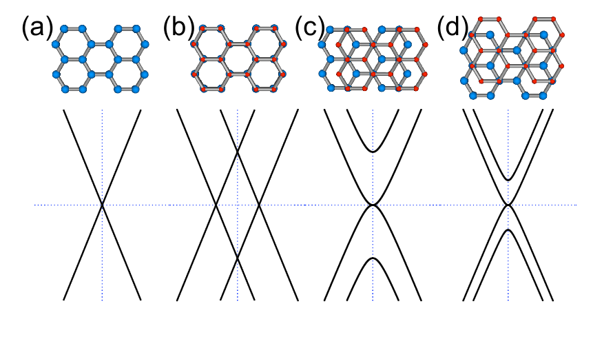
As we are interested in the transport properties of the bilayer flakes, we will concentrate on structures where the leads are monolayer armchair graphene nanoribbons (aGNR), with widths chosen to have metallic character. We denote the ribbon width with an integer indicating the number of carbon dimers along it. With this convention, a nanoribbon of width , where , is metallic. In Fig. 2(a) we plot the atomic geometry of the monolayer aGNR leads and the corresponding low energy electronic bands, as obtained from the tight-binding Hamiltonian. Note that in aGNR the two Dirac points collapse in just one. [10] Near the Dirac point the dispersion is linear, . In the transport calculations we will only consider incident electrons inside this subband, i.e., with energy lower than the second subband. An aGNR is metallic because of a particular combination of the wavefunctions coming form the two original Dirac points. This combination is preserved when piling up two metallic armchair monolayer ribbons, being the corresponding bilayer nanoribbon also metallic.
The details of the low energy spectrum of bilayer nanoribbons depend on the particular stacking. In Fig. 2(b) we plot the tight-binding band structure of a bilayer nanorribon with stacking. The bands also present a linear dispersion and they can be understood as bonding/antibonding combinations of the constituent monolayer aGNR bands.
The stacking can be achieved from the bilayer geometry by displacing one graphene monolayer with respect to the other, in such a way that the atoms of one sublattice (i.e., ) of the top monolayer are placed over the atoms of the other sublattice () of the bottom monolayer. In nanoribbons, two different stackings are possible:[Sahu_2008] the - stacking, shown in Fig. 2(c), which yields a more symmetric geometry for infinite armchair nanoribbons, and the - stacking, shown in 2(d). Notice that, for armchair nanoribbons, the - configuration can be reached by displacing the top monolayer in the direct stacking a distance equal to the carbon-carbon bond along the ribbon length, as can be seen by comparing Figs. 2(b) and (c). For the - stacking, the displacement is of the same magnitude but at 60o with the ribbon longitudinal direction, yielding a less symmetric configuration for armchair nanoribbons (Fig. 2(d)). In both cases the -stacked bilayer graphene nanoribbons have metallic character, and the conduction and valence bands have a parabolic dispersion at the Dirac point.
II.2 Dirac-like Hamiltonians
Most of the low energy properties of monolayer and bilayer graphene nanoribbons can be understood using a approximation, which yields a Dirac-like Hamiltonian. [10, 11, 25] The low-energy effective bilayer Hamiltonian describing the properties of a infinite -stacked bilayer has the form
| (3) |
where , , and is the momentum relative to the Dirac point. The Hamiltonian acts on a four-component spinor . The eigenfunctions of this Hamiltonian are bonding and antibonding combinations of the isolated graphene sheet solutions,
| (4) |
with .
The low-energy Hamiltonian of the stacking reads[14]
| (5) |
with eigenvalues
| (6) |
For a given eigenvalue ,the wavefunction takes the form
| (7) |
In accordance with the geometry shown in Fig. 1, we assume for nanoribbons that the system is invariant in the direction, and therefore is a good quantum number. In the case of metallic aGNR, the boundary conditions are satisfied[10] for 0 independently of the nanoribbon width; this 0 state is the lowest energy band confined in the aGNR. We have checked that the dispersion of the lowest energy band obtained by solving the Dirac model coincides with that obtained by diagonalizing the tight-binding Hamiltonian for the monolayer, bilayer and - nanoribbons. Therefore, the Dirac approximation is a good description for the low energy properties of these nanoribbons, Fig. 2(a)-(c). This is not the situation for bilayer graphene nanoribbons with - stacking. In this case, the atomic asymmetry at the edges of the ribbon is not captured by the Dirac model, which is a long-wavelength approximation. Therefore, we should describe the electronic properties of nanoribbons with - stacking using the tight-binding Hamiltonian.
III Conductance
III.1 Tight-Binding approach: Landauer-Büttiker formalism
Due to the lack of translational invariance of the system, in the tight binding model we calculate the electronic and transport properties using the surface Green function matching method.[31, 32] To this end, the system is partitioned in three blocks: two leads, which we assume to be semi-infinite aGNR, and the conductor, consisting of the bilayer flake. The Hamiltonian is
| (8) |
where , , and are the Hamiltonians of the central portion, left and right leads respectively, and , are the coupling matrix elements from the left and right lead to the central region . The Green function of the conductor is
| (9) |
where is the selfenergy due to lead , and is the Green function of the semi-infinite lead . [33]
In the linear response regime, the conductance can be calculated within the Landauer formalism as a function of the energy . In terms of the Green function of the system,[34, 31, 32] it reads
| (10) |
where , is the transmission function across the conductor, and is the coupling between the conductor and the lead.
III.2 Continuous approximation: wavefunction matching
In the low-energy limit, we can obtain the conductance of the system by matching the eigenfunctions of the Dirac-like Hamiltonians. As commented above, we consider incident electrons from the lowest energy subband, which correspond to a transversal momentum =0 in aGNRs. Assuming an electron with energy coming from the left monolayer ribbon, we compute the transmission coefficient to the right monolayer lead. In the central part the wavefunctions are linear combinations of the solutions of the bilayer nanoribbon Hamiltonians given in Sec. II.2 at the incoming energy . The transmission, reflection and the coefficients of the wavefunctions in the bilayer part are determined by imposing the appropriate boundary conditions at the beginning () and at the end () of the bilayer region. Matching of the wavefunctions amounts to require their continuity. As the Hamiltonian is a first-order differential equation, current conservation is ensured automatically. The precise boundary condition depends both on the lead configuration ( or ) and on the stacking.
III.2.1 AA stacking
In this stacking, each atom has an atom on top of it. The dispersion in the central part is given by Eq. (4), and for each incident carrier with momentum , there are always two reflected and two transmitted eigenfunctions with momenta ; see Fig. 2(b).
In the (bottom-bottom) configuration the wavefunction should be continuous in the bottom layer, i.e. continuous at and continuous at ; for the top layer
| (11) |
From these boundary conditions we obtain the transmission
| (12) |
In the configuration the bottom wavefunction and the top wavefunction should be continuous at and respectively. In addition, the hard-wall condition should be satisfied:
| (13) |
The above boundary conditions yield the transmission
| (14) |
We see from these equations that the conductance changes periodically as function of the incident energy and length of the bilayer flake. For fixed , the transmission is a periodic function of the incident energy. In the bottom-bottom geometry there are antiresonances, =0, at energies given by , with . These energies corresponds to quasilocalized states in the top part of the bilayer flake. [35] The paths through the bottom graphene ribbon and through the quasilocalized state of the top flake interfere destructively, producing the antiresonance. [36, 37, 38, 39] In the bottom-top configuration, the momenta of the quasilocalized states of the bilayer flake are shifted in , so the antiresonances occur at energies , with .
For fixed energy, the conductance varies periodically with the length of the bilayer flake. There is a period, , related to the energy of the incident carrier; other periods are harmonics of that imposed by the interlayer hopping, . The dependence of the conductivity on can be understood by resorting to a simple non-chiral model with linear dispersion. Consider an incident carrier from the left with momentum and energy in the bottom sheet. When arriving at the bilayer central region, the incident wavefunction decomposes into a combination of bonding () and antibonding () states of the bilayer with momentum = . The conductance through the bilayer region is proportional to the probability of finding an electron at the top (bottom) end of the central region, , depending of whether the system is in the or in the configuration. This simple model explains the dependence of the conductivity on harmonics of and also why the and the transmissions are in counterphase. The phase opposition is more evident in the limit of Eqs. (12) and (14), which give an conductance in the bottom-top configuration equal to zero, whereas in the bottom-bottom configuration it has a maximum finite value that depends on the flake size:
| (15) |
| (16) |
III.2.2 AB stacking
In this stacking only the atoms of layer and the atoms of layer are directly connected by tunneling. The dispersion in the central part is given by Eq. (6). For an incident carrier with and momentum there are always two reflected and two transmitted eigenfunctions with momentum in the bilayer region, see Fig. 2(c). However, for incident wavefunctions with , there are only one reflected and one transmitted central wavefunctions with momenta . In addition, there are an evanescent and a growing state with decay constants . Therefore, the conductance of the system depends on whether the energy of the carrier is larger or smaller than the interlayer hopping. For , there are two channels in the central region and the interference between these channels produces antiresonances, whereas for only an electronic channel is present in the central region, and Fabry-Perot interference can occur. Analytical, but very large and impractical expressions can be obtained for the conductance in the stacking. Therefore, we choose to present the expressions for the transmission in the low and high energy limit. In the next section, when comparing with the tight-binding results, we plot the exact results obtained from wavefunction matching in the continuum approximation.
The boundary conditions for stacking in the bottom-bottom configuration are similar to those of the AA case: and should be continuous at and respectively, and
| (17) |
In the low energy limit, , the stacking conductance in the bottom-bottom configuration takes the form
| (18) |
which presents resonances when ; for large this occurs when , being an integer. For the system has transmission unity.
In the limit of large energy, and in the bottom-bottom configuration the transmission is
| (19) |
This transmission presents antiresonances associated with destructive interferences of the two electronic paths in the bilayer region. The behavior of the conductance is similar to that of the stacking, Eq. (12). There are periodicities associated with the energy of the incident electron: for , ; and there are also periodicities associated with the interlayer hopping. The lower harmonic in the stacking, , is half the basic harmonic in the stacking, and this reflects the fact that in the stacking only half of the atoms have direct interlayer tunneling.
In the bottom-top geometry and should be continuous at and respectively, and
| (20) |
In the stacking, interlayer tunneling connects atoms with atoms; this arrangement determines the form of Eq. (20).
For the bottom-top transmission can be approximated as
| (21) |
It can be seen that the conductance goes to zero when For , tends to zero, and it is complementary to . For large , presents resonances at , with integer. For energies larger than the interlayer hopping the conductance can be approximated as
| (22) |
In this energy limit, the interference between different electron paths through the systems produces antiresonances. Similarly to the bottom-bottom configuration, for a fixed energy the transmission varies periodically with , with one period given by the incident energy, , and others related to the interlayer hopping, .
IV Results
As the systems possess electron-hole symmetry, we concentrate on energies . Let us recall here that the length of a unit cell (u.c.) for an armchair ribbon is . In the following Figures, we choose to give the system length in terms of the armchair ribbon u.c. length, which is unambiguous for the discrete tight-binding model. Note that, in the continuum approximation, the hard wall conditions at the edges of the system ( and ) are set at two extra rows of atoms where the wavefunctions are imposed to be zero. This amounts to add to the system length the quantity , which we take into account when comparing the continuum and the tight-binding results.
IV.1 and - stackings
As discussed in the previous Section, the expressions for the transmission (Eqs. (12), (14), (18), (21), (19), and (22)) demonstrate that the dependence with the system length has periodicities related to the interlayer coupling . This is evident in Fig. 3, which shows the length dependence of the conductance at a fixed energy , for the stackings and AB- and the two lead configurations, and . Here we depict the tight-binding results with circles and the continuum ones with full lines. The tight-binding calculations are performed for a ribbon of width , but for this energy range only one channel contributes to the conductance in the monolayer and at most two channels in the bilayer flake, so the conductance is independent of . The agreement between the two models is excellent for these stackings and energy range. As expected, the stacking shows clear antiresonances as a function of length, and the results for the and configurations are exactly in counterphase.
The results for the two configurations ( and ) with - stacking have an approximate complementarity; only at there is zero transmission for the case corresponding to a transmission maximum for the system. The subsequent maxima and minima are slightly shifted, and more importantly, there are no zero antiresonances for finite length. As mentioned before, there is only one transmission channel in the bilayer, so although the conductance oscillates due to finite-size effects, there are not antiresonances for the - at this energy.
Fig. 4 shows the length dependence of the conductance for another energy , where there are two conducting channels for both stackings. It is apparent the change for the AB- case, which now presents antiresonances with zero conductance. As to the stacking, the conductance for the configuration shows only one clear period of 16 u.c., whereas the case shows also a 8 u.c. periodicity, stemming from the term in the conductance. The analytical expressions Eqs. (12) and (14) allows us to verify that, for the case, this energy-dependent term combines with the other -dependent terms to yield a single period, whereas for the case, the survives.
Figure 5 shows the conductance as a function of energy for the two geometries considered and the most symmetric stackings, namely the and the -, for a flake length of u.c. (top panel) and u.c. (bottom panel). The tight-binding results are depicted with circles and the continuum ones with lines.
As discussed before, the most characteristic feature of the transmission is the appearance of Fano antiresonances with zero conductance. This can happen for any energy in the case of stacking because there are always two conducting channels in the bilayer. On the contrary, for - stacking, with only one channel for , the oscillations in the conductance are due to a Fabry-Perot-like effect, i.e., the interference of one scattering channel with itself due to the finite size of the structure. This is most clearly seen for the case, where the - stacking presents a non-zero minimum in the conductance in the energy range, whereas the antiresonances above clearly reach zero values.
Notice as well the agreement with the continuum calculations when . All the configurations have zero conductance in this limit. As to the configuration, has a in general nonzero value, which oscillates as a function of the system length, as described by Eq. (15) and it is seen in Fig. 5. The and results for the stacking do show a certain complementarity: the conductance minima in one configuration coincide with the maxima of the other one. Furthermore, the periodicity of the conductance as a function of energy for the stacking due to the term is evident in Fig. 5, and agrees perfectly with the value given by the Dirac continuum approximation, namely 0.16 for and 0.079 for .
The continuum model allows us to make a more complete characterization of the behavior of these systems. Fig. 6 shows contour plots of the transmission versus energy and bilayer flake length for the direct stacking and the two configurations, and , given by Eqs. (12) and (14). We clearly see the main transmission antiresonances with a 16 u.c. period, stemming from the interlayer hopping term , as discussed in Sec. III.2.1. In fact, it turns out that for certain flake sizes , the conductance is zero, independently of the energy. As this spatial period depends directly on the interlayer coupling strength , we propose that this feature can be used to measure the interlayer hopping parameter, the value of which is still under debate:[40] by overlapping two nanoribbons and displacing one of them with respect to the other, the spatial period could be measured and thus would be obtained.
As the variation of the conductance as a function of length is so dramatic, from one quantum of conductance to zero, this system can function as an electromechanical switch, turning from the maximum conductance to zero by a displacement of a few Å. The contour plots for the case also reveal the counterphase behavior of the and configuration discussed previously. It is patent how the maxima of the conductance vs. L for the system coincide with the minima and viceversa.


Fig. 7 displays the contour plots for the - case obtained within the Dirac model. There are two important differences with respect to the stacking. First, now there are two distinct energy regions, set by the interlayer coupling . Below , there are no antiresonances because there is only one propagating channel at the bilayer. There are conductance oscillations, but not so marked as for , where the zero antiresonances appear because of the coexistence of two propagating eigenchannels in the bilayer flake. For this energy range, the behavior is more similar to that found for the stacking, with an obvious difference on the spatial periods. As already mentioned in Sec. III.2.2, the lower harmonic in the stacking is , thus yielding a longer spatial period (32 u.c.) that we attribute to the smaller coupling between layers for this case.
IV.2 - stacking
Until this point, we have focused in the more symmetric stackings, for which the continuum Dirac model and the tight-binding have an excellent agreement, as demonstrated. Now we turn our attention to the - stacking, which we can only model adequately with the tight-binding approach. This is because of the lack of symmetry of the ribbon edges, as it can be seen in Fig. 2 (d). The atoms at the upper egde of the top layer are not connected to the atoms of the bottom layer, independently of the sublattice they belong, and viceversa. Such a feature cannot be well described by the continuum Dirac Hamiltonian given by Eq. (5), which assumes that all carbon atoms in the sublattice of the bottom layer are connected to the atoms on the top layer. This difference is not very important for wide ribbons, but it is noticeable for the narrow cases, for which the proportion of atoms at the ribbon edges is non-negligible.
One way to assess the importance of the edge effect is to check the energy difference between the first and the second subband for . For a - nanoribbon is always , whereas for - nanoribbons it depends on the ribbon width, as it can be seen in Figs. 2 (c) and (d). Size effects are related to the ratio of atoms which are not well described by the continuum Hamiltonian of Eq. (5). This brings in a dependence on the ribbon width, as shown in Fig. 8, depicting the conductance for three energies and ribbon widths for the two configurations, and . Notice the dependence on the ribbon width; the conductance results demonstrate that size effects are still important for . For the lowest energy depicted, for which there is only one propagating channel in the bilayer flake, the three widths show a similar behavior for sufficiently long flakes (). However, for the highest energies the disagreement is patent, due to the dependence of the longest spatial period on the system width. The different periods are more clear for the energy , for which at least half a wavelength of the oscillation can be appreciated for the three ribbon widths. Notice that the case , shown in the central part of both panels in Fig. 8, is also depicted for the - stacking in Fig. 3. This striking difference in the conductance for the two stackings is due to the fact that in the - case theres is only one channel for this energy, whereas in the - there are already two.
V Summary
In this work, we have studied the conductance of a graphene bilayer flake contacted by two monolayer nanoribbons. Two contact geometries have been considered: either the left and right lead are contacted to the same layer of the flake or to opposite layers. Furthermore, three different stackings for the graphene flake have been taken into account, namely, , - and -.
We have calculated the conductance with a tight-binding approach and also by performing a mode-matching calculation within the continuum Dirac model, by choosing the appropriate boundary conditions. We have explained the features in the transmission and obtained analytical expressions that allow us to elucidate the transport characteristics of these structures. We have found several periodicities on the conductance, related to the energy and the interlayer coupling of the system.
In particular, for the configuration, we have found that the conductance through the flake shows Fano antiresonances, that we have related to the interference of two different propagating channels in the structure. For a flake of length , the main transmission period is given by . For a fixed incident energy, the conductance as a function of the system length oscillates with two main periods related to the energy and the interlayer coupling .
For the stacking, we have found two distinct behaviors as a function of the incident energy : for energies larger than the interlayer hopping , the transmissions resemble those found for the stacking. This is due to the existence of two propagating channels at this energy range. There is, however, a difference on the main period related to the interlayer hopping , which is twice the period found for the stacking. This can be understood by noticing that in the stacking only half of the atoms are connected between the two graphene layers. For energies smaller than , the -stacked flake only has one eigenchannel, and the conductance shows resonances related to the existence of Fabry-Parot-like states in the system.
The conductance of these bilayer flakes can oscillate between zero and the maximum conductance as a function of length; thus, a system composed by two overlapping nanoribbons can behave as an electromechanical switch. We propose that these characteristics can be employed to measure the interlayer hopping in bilayer graphene. Our results constitute a comprehensive view of transport through bilayer graphene flakes, clarifying the role of stacking, contact geometries, flake width and length in the conductance of these structures.
Acknowledgments
This work has been partially supported by the Spanish DGES under grants MAT2006-06242, MAT2006-03741, FIS2009-08744 and Spanish CSIC under grant PI 200860I048. J.W.G. would like to gratefully acknowledge helpful discussion to Dr. L. Rosales, to the ICMM-CSIC for their hospitality and MESEUP research internship program. J.W.G. and M.P. acknowledge the financial support of CONICYT/Programa Bicentenario de Ciencia y Tecnología (CENAVA, grant ACT27) and USM 110856 internal grant.
References
- [1] K.S.Novoselov, A.K.Geim, S.V.Mozorov, D.Jiang, Y.Zhang, S.V.Dubonos, I.V.Gregorieva, and A.A.Firsov, Science 306, 666 (2004).
- [2] A. H. Castro-Neto, F.Guinea, N.M.R.Peres, K.S.Novoselov, and A.K.Geim, Rev. Mod. Phys. 81, 109 (2009).
- [3] K.S.Novoselov, D.Jiang, T.Booth, V. Khotkevich, S. M. Morozov, and A.K.Geim, Nature 438, 197 (2005).
- [4] Y. Zhang, Y.-W. Tan, H. L. Stormer, and P. Kim, Nature 438, 201 (2005).
- [5] A. F. Young and P. Kim, Nature Phys. 5, 222 (2009).
- [6] N. Stander, B. Huard, and D. Goldhaber-Gordon, Phys. Rev. Lett. 102, 026807 (2009).
- [7] K. Nakada, M. Fujita, G. Dresselhaus, and M. S. Dresselhaus, Phys. Rev. B 54, 17954 (1996).
- [8] M.Fujita, K. Wakabayashi, K.Nakada, and K.Kusakabe, J.Phys. Soc. Jpn. 65, 1920 (1996).
- [9] K. Wakabayashi, M. Fujita, H. Ajiki, and M. Sigrist, Phys. Rev. B 59, 8271 (1999).
- [10] L. Brey and H. Fertig, Phys. Rev. B 73, 235411 (2006a).
- [11] L. Brey and H. Fertig, Phys. Rev. B 73, 195408 (2006b).
- [12] A. R. Akhmerov and C. W. J. Beenakker, Phys. Rev. B 77, 085423 (2008).
- [13] A. Iyengar, T. Luo, H. A. Fertig, and L. Brey, Phys.Rev.B 78, 235411 (2008).
- [14] E. McCann and V. I. Fal’ko, Phys. Rev. Lett. 96, 086805 (2006).
- [15] F. Guinea, A. H. C. Neto, and N. M. R. Peres, Phys. Rev. B 73, 245426 (2006).
- [16] E. V. Castro, K. S. Novoselov, S. V. Morozov, N. M. R. Peres, J. M. B. L. dos Santos, J. Nilsson, F. Guinea, A. K. Geim, and A. H. C. Neto, Phys. Rev. Lett. 99, 216802 (2007).
- [17] H. V. Roy, C. Kallinger, and K. Sattler, Surface Science 407, 1 (1998).
- [18] J.-K. Lee, S.-C. Lee, J.-P. Ahn, S.-C. Kim, J. I. B. Wilson, and P. John, The Journal of Chemical Physics 129, 234709 (2008).
- [19] Z. Liu, K. Suenaga, P. J. F. Harris, and S. Iijima, Phys. Rev. Lett. 102, 015501 (2009).
- [20] M. Hanfland, H. Beister, and K. Syassen, Phys. Rev. B 39, 12598 (1989).
- [21] J.-C. Charlier, X. Gonze, and J.-P. Michenaud, EPL (Europhysics Letters) 28, 403 (1994).
- [22] A. H. R. Palser, Phys. Chem. Chem. Phys. 1, 4459 (1999).
- [23] Y. Xu, X. Li, and J. Dong, Nanotechnology 21, 065711 (2010).
- [24] H. Min, B. Sahu, S. K. Banerjee, and A. H. MacDonald, Phys. Rev. B 75, 155115 (2007).
- [25] J. Nilsson, A. H. Castro Neto, F. Guinea, and N. M. R. Peres, Phys. Rev. B 76, 165416 (2007).
- [26] I. Snyman and C. W. J. Beenakker, Phys. Rev. B 75, 045322 (2007).
- [27] Y.-M. Lin and P. Avouris, Nano Lett. 8, 2119 (2008).
- [28] B. Sahu, H. Min, and S. K. Banerjee, eprint cond-mat/0910.2719.
- [29] T. Ohta, A. Bostwick, T. Seyller, K. Horn, and E. Rotenberg, Science 313, 951 (2006).
- [30] L. M. Malard, J. Nilsson, D. C. Elias, J. C. Brant, F. Plentz, E. S. Alves, A. H. C. Neto, and M. A. Pimenta, Phys. Rev. B 76, 201401 (2007).
- [31] L. Chico, L. X. Benedict, S. G. Louie, and M. L. Cohen, Phys. Rev. B 54, 2600 (1996).
- [32] M. B. Nardelli, Phys. Rev. B 60, 7828 (1999).
- [33] L. Rosales, M. Pacheco, Z. Barticevic, A. Latgé, and P. Orellana, Nanotechnology 19, 065402 (2008).
- [34] S. Datta, Electronic Transport in Mesoscopic Systems (Cambridge University Press, Cambridge, 1995).
- [35] Note that for a metallic monolayer nanoribbon in the single mode approximation (=0), localized states appear whenever the longitudinal moment times the length of the bar satisfies =0; see Ref. 10.
- [36] E. Tekman and P. F. Bagwell, Phys. Rev. B 48, 2553 (1993).
- [37] A. A. Clerk, X. Waintal, and P. W. Brouwer, Phys. Rev. Lett. 86, 4636 (2001).
- [38] X. R. Wang, Y. Wang, and Z. Z. Sun, Phys. Rev. B 65, 193402 (2002).
- [39] P. A. Orellana, F. Domínguez-Adame, I. Gómez, and M. L. Ladrón de Guevara, Phys. Rev. B 67, 085321 (2003).
- [40] J. Nilsson, A. H. C. Neto, N. M. R. Peres, and F. Guinea, Phys. Rev. B 73, 214418 (2006).