Coulomb-induced Rashba spin-orbit coupling in semiconductor quantum wells
Abstract
In the absence of an external field, the Rashba spin-orbit interaction (SOI) in a two-dimensional electron gas in a semiconductor quantum well arises entirely from the screened electrostatic potential of ionized donors. We adjust the wave functions of a quantum well so that electrons occupying the first (lowest) subband conserve their spin projection along the growth axis (), while the electrons occupying the second subband precess due to Rashba SOI. Such a specially designed quantum well may be used as a spin relaxation trigger: electrons conserve when the applied voltage (or current) is lower than a certain threshold ; higher voltage switches on the Dyakonov-Perel spin relaxation.
Keywords:
spin-orbit interaction, Rashba, modulated quantum wellspacs
72.25.Dc, 72.25.Rb, 73.21.FgIntroduction.
The ability to control the amplitude of the Rashba[1] spin-orbit interaction (SOI) electrically[2, 3] makes this type of SOI one of the most promising instruments for manipulating spins of electrons in future spintronic devices[4, 5]. The most commonly studied case is the Rashba SOI in a two-dimensional electron gas (2DEG) inside a symmetrical quantum well. In such a system the Rashba SOI is zero in the absence of an external electric field, applied perpendicularly to the plane of the quantum well. Further, in a quantum well with more than one subband, such external-field induced spin-orbit coupling does not show strong dependence on the subband index.
It is natural to ask whether Rashba SOI can also appear in the absence of an external electric field. A well-known argument,[6] based on the Ehrenfest theorem, leads to the conclusion that this cannot happen, as long as the confinement potential for the valence band is proportional to the confinement potential for the conduction band (which is usually the case). However, this argument fails to take into account the screened electrostatic potential of the donors: this breaks the proportionality between the potentials acting on electrons and holes and leads to a finite SOI in the absence of an external field. We describe this effect as Coulomb-induced Rashba SOI.
An attractive feature of the Coulomb-induced Rashba SOI is that it can be made strongly subband-dependent by a proper engineering of the shape of the quantum well. In this letter we use techniques of inverse scattering theory[7] to find a shape of the quantum well for which the first (lowest) subband is free of SOI, while the second has a rather large SOI. We suggest that such a shape may be realized by digital alloying techniques. In such a specially engineered quantum well, electrons in the lowest subband would conserve their spin projection along the growth axis ([110]), but electrons in the second subband would suffer spin relaxation by Dyakonov-Perel mechanism. More importantly, we suggest that a parallel electric field (as opposed to the conventional perpendicular electric field) might be used to control the SOI amplitude by “pumping” electrons into the second subband. The electrostatic potential generated by this non-equilibrium population would “turn-on” the Rashba coupling, leading to Dyakonov-Perel spin relaxation also in the lowest subband.
The model.
We consider a two-dimensional electron gas confined within a quantum well (QW) in an AlxGa1-xAs heterostructure (see Fig. 1).
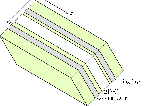
We assume that the electrons in the QW are provided by donors outside the well, and that the concentration of donors is high enough so that the 2DEG is degenerate. The electronic states in the well are plane waves with momentum in the plane of the well . They are further characterized by a subband index , which determines the transverse envelope wave function . Our QW contains only two subbands for electrons, or , and only the lowest subband () is populated in equilibrium.
If the quantum well is grown along the [110] direction, the Dresselhaus[8] spin-orbit interaction is absent, and the main source of spin relaxation is the Rashba[9] spin-orbit interaction,
| (1) |
where the SOI amplitude is given by
| (2) |
is the complete[10] potential acting on the holes[2], is the fundamental band gap, , is the spin-orbit splitting of the valence band, is the matrix element of momentum between and atomic states, and are subband envelope functions. Apart from the bare valence band confinement and a possible external potential (such as the one that arises from a perpendicular electric field), includes the self-consistent “Hartree” potential induced by the donors and the inhomogeneous charge distribution inside the well:
| (3) |
For , the confinement potential in the valence band of AlxGa1-xAs is proportional[2, 11] to the confinement potential, , in the conduction band:
| (4) |
Setting and making use of Eq. (4) we can write
| (5) |
where is the full potential acting on the electrons. The expectation value of the force in the state vanishes by the Ehrenfest theorem, so that only the contribution from the Hartree potential survives. We conclude that, in the absence of external fields, the Rashba SOI is produced entirely by the Coulomb contribution to the hole potential,
| (6) |
where is obtained from the self-consistent solution of both Schrödinger and Poisson equations for the electron envelope functions . It is evident from (6) that the SOI vanishes in all subbands if the confinement potential and the donor distribution are symmetric. The reason is that in this case is an odd function of , while the envelope function has a definite parity.
Spin-orbit coupling engineering.
When the confinement potential and/or the donor distribution is asymmetric, both SOI amplitudes and are, in general, non-zero. In order to eliminate the Dyakonov-Perel relaxation in equilibrium, we have to engineer a confinement for which[12] but . This can not be achieved by breaking the symmetry of either or ; one has to break both symmetries, so that
| (7) |
We proceed as follows: first we introduce a slight asymmetry in the positioning of the doping layers with respect to the center of the well, thus breaking the symmetry of (see Figs. 1 and 3). On top of that, we utilize a technique of inverse scattering theory known as Double Darboux Transformation (DDT),[7] to generate an asymmetric confinement potential , which satisfies the first of inequalities (7).
In a DDT one changes the single particle potential and the wave functions in such a way that the eigenvalues are preserved. This, in turn, offers a way to significantly modify the strengths of the SOI amplitudes without grossly altering the spectrum of the quantum well. Naturally, the invariance of the eigenvalues under the DDT is rigorous only if electron-electron interactions are neglected. However, we have found that, even in the presence of interactions, the variation of the eigenvalues remains relatively small, about .
The precise form of the transformation is[7]
| (8) |
where is the original (symmetric) confinement, and are the corresponding wave functions (WFs). The parameter measures the strength of the symmetry breaking of ; corresponds to the identity transformation, i.e., and . We assumed in (8) that and . We further assume that represents a rectangular well parameterized by (height) and (width).

In Fig. 2 we show the dependence of and on the parameter . We see that when . At this value of we have in the chosen units. The form of the confinement potential at this value of is shown in Fig. 3, together with the plot of the electron envelope functions for the two subbands. Such a potential might be realized by MBE techniques.[14] When only the lowest subband in this specially engineered QW is populated, the electrons do not suffer spin relaxation. This happens in equilibrium, when the energy distribution of electrons everywhere in the sample is given by a Fermi function. When the sample is driven out of equilibrium (e.g., by the current or by light illumination), so that both bands are populated, the SOI effects are activated.

Changing the population of the subbands.
It is well-known[15] that the Rashba SOI amplitude can be controlled by a perpendicular (to the QW plane) electric field. Below we show that an electric field which drives a current in the plane of the QW, can be used as a “switch” for the SOI amplitude, when this amplitude is initially set to zero by the method described in the previous section.
Under ordinary conditions, when a current flows in an electron gas, in the linear response regime, strong inelastic interactions among the electrons and between electrons and phonons establish a local equilibrium distribution, controlled by a local (position-dependent) electrochemical potential :
| (9) |
where is the direction along the current, is the sample length, and are the electrochemical potentials in the left and right contacts, and is the applied voltage. Similar to , also the subband energies and the density of states depend on the coordinate,
| (10) |
where , so that the concentration of electrons remains independent of position.
However, in a mesoscopic sample at small temperatures and high mobility values, when the condition is satisfied, where is the diffusion constant and is the inelastic scattering from electron-electron and electron-phonon interactions, the energy relaxation effects are so small that an electron may pass through the entire sample conserving its energy. This results in a two-step form of an energy distribution function inside the sample,[16, 17] see Fig. 4:
| (11) |
where and are Fermi energy distributions in the left and right contacts attached to the sample, respectively.

When the voltage across the sample exceeds the critical value , the energy of the “hot” electrons from the right contact exceeds the energy of the bottom of the second subband on the left end of the device. The fraction of such “hot” electrons is controlled by (11): it is maximal near the right contact and vanishes in the vicinity of the left contact. More precisely, the -dependent population of the second subband is (see Fig. 5)
| (12) |
where , and is the total density of electrons. In (12) we assumed that electrons spread equally between the bands when their energy allows them to be either in first or the second subband.
In equilibrium, the second subband would remain unpopulated everywhere in the sample since for arbitrary . In a steady (non-equilibrium) current-carrying state, there is a zone inside the sample, where both subbands are populated. The width of this zone is controlled by the applied voltage, see Fig. 5.
The electric field-induced change in the population of the subbands modifies the Hartree potential , which in turn modifies the values of and . In particular becomes non-zero when the voltage exceeds a critical value ( for ), with the other parameters being specified in the caption of Fig. 3. The coordinate dependence of and for different voltages is shown in Fig. (6).

We conclude that the Dyakonov-Perel spin relaxation of electrons in the lowest (majority) subband can be switched on by an electric field (or a current) in the plane of the QW. It is essential for the argument that this field does not modify the envelope functions of the electrons. The field affects due to the subband repopulation, and the effect is large only because had previously been fine-tuned to be zero.
Discussion.
The method described in this Letter allows in principle to quickly suppress a spin polarization by applying a current. A crucial point is the feasibility of keeping the hot electrons hot (i.e., to avoid thermalization). One way to ensure this is to use short wires, low temperatures and high mobilities, so that the condition is satisfied. Failing this, another possibility would be to rely on the nonlinear hot electron effect, see p.120 in [18], whereby, in the presence of strong inelastic scattering, the distribution at the center of the sample is a Fermi distribution with an effective temperature . If is sufficiently large, this will produce the desired population of the higher subband. Finally, we notice that, while our treatment has neglected the intrinsic Dresselhaus SOI, the latter’s action may be compensated by a Rashba SOI having the same amplitude, so that becomes a conserved quantity.[19] So the proposed scheme should work even in the presence of Dresselhaus spin-orbit interaction.
We acknowledge the support of ARO Grant No. W911NF-08-1-0317. We thank Michael Flatté for helpful discussions.
References
- [1] Y. A. Bychkov and E. I. Rashba, JETP Lett. 39, 66 (1984).
- [2] R. Winkler, Spin-Orbit Effects in Two-Dimensional Electron and Hole Systems (Springer, 2003).
- [3] G. Bastard, J. A. Brum, and R. Ferreira, Solid State Physics 44, 229 (1991).
- [4] D. D. Awschalom, D. Loss, and N. Samarth, eds., Semiconductor Spintronics and Quantum Computation (Springer, 2002).
- [5] D. D. Awschalom and M. E. Flatté, Nature Physics 3, 153 (2007).
- [6] R. Winkler, Physica E: Low-dimensional Systems and Nanostructures 22, 450 (2004), 15th International Conference on Electronic Propreties of Two-Dimensional Systems (EP2DS-15).
- [7] B. N. Zakhariev and V. M. Chabanov, Submissive quantum mechanics (Nova Science, New York, 2007).
- [8] G. Dresselhaus, Phys. Rev. 100, 580 (1955).
- [9] N. S. Averkiev, L. E. Golub, and M. Willander, J. Phys.: Condens. Matter 14, R271 (2002).
- [10] R. S. Calsaverini, E. Bernardes, J. C. Egues, and D. Loss, Phys. Rev. B 78, 155313 (2008).
- [11] J. H. Davies, The physics of low-dimensional Semiconductors (Cambridge Univ. Press, 1997).
- [12] In a situation when and , there is an important contribution to the SOI amplitude due to microscopic fluctuations of the donor concentration[20]. In our case this contribution is estimated to be extremely small, relative to the usual Rashba contribution.
- [13] All figures in this article were calculated by the programs available from http://shalaev.pochta.ru/1001.html and http://quantumtheory.physik.unibas.ch/shalaev/1001.html.
- [14] A. C. Gossard, M. Sundaram, and P. F. Hopkins, Semiconductors and Semimetals (Academic, Boston MA, 1994), vol. 42, p. 153.
- [15] E. I. Rashba, Physica E 20, 189 (2004).
- [16] H. Pothier, S. Guéron, N. O. Birge, D. Esteve, and M. H. Devoret, Phys. Rev. Lett. 79, 3490 (1997).
- [17] A. Kamenev, arXiv:cond-mat/0412296.
- [18] Y. M. Blanter and M. Büttiker, Physics Reports 336, 1 (2000).
- [19] O. Chalaev and D. Loss, arXiv:cond-mat/0407342.
- [20] M. M. Glazov and E. Y. Sherman, Phys. Rev. B 71, 241312 (2005).