Hybrid density functional calculations of the band gap of GaxIn1-xN
Abstract
Recent theoretical work has provided evidence that hybrid functionals, which include a fraction of exact (Hartree Fock) exchange in the density functional theory (DFT) exchange and correlation terms, significantly improve the description of band gaps of semiconductors compared with local and semilocal approximations. Based on a recently developed order- method for calculating the exact exchange in extended insulating systems, we have implemented an efficient scheme to determine the hybrid functional band gap. We use this scheme to study the band gap and other electronic properties of the ternary compound In1-xGaxN using a 64-atom supercell model.
pacs
71.15.DX, 71.15.Mb, 71.20.NrThe design of novel functional semiconductors with given values of the energy band gap is an area of intense research [1, 2, 3, 4, 5]. In particular, much attention is focused on the band gap engineering of group-III nitride semiconductors, whose remarkable optical properties are important for optoelectronic device applications [6, 7]. To guide the search for compounds with tailored properties [1], experimental studies are often accompanied by electronic structure calculations based on density functional theory (DFT) [8]. For these calculations, the local-density(LDA) or generalized gradient approximations(GGA) are typically used. Due to the delocalization error of the LDA and GGA exchange and correlation functionals, however, these approaches severely underestimate the materials band gaps [9, 10].
As shown by several recent studies [11], a significant improvement in the description of semiconductor and insulator band gaps is generally obtained by using hybrid functionals [12], in which some exact (Hartree-Fock) exchange is mixed into the exchange and correlation functional. This reduces the delocalization and derivative discontinuity errors of (semi)local functionals [9, 10, 2, 11]. However, because of the considerable computational cost of evaluating the non-local exact exchange term, hybrid functionals have been mostly applied to systems with small unit cells [13]. For the modeling of systems where a large supercell is needed, an additional screened exchange approximation is usually made to relieve the computational burden [2, 11].
Recently Wu et al. (WSC) [14] introduced an order- method to calculate the exact exchange in extended insulating systems. The WSC method is based on a localized Wannier function representation of the occupied (valence) space, so that the exchange interaction between two orbitals decays rapidly with the distance between their centers. A truncation can thus be introduced, which greatly reduces the computational cost. The effectiveness of the WSC method was demonstrated by ground state electronic minimizations for crystalline silicon in supercells with 64 and 216 atoms.
In this paper, we extend the WSC scheme to compute hybrid functional band gaps. To this end, the system’s first (few) empty conduction state(s) is(are) determined starting from the ground state calculated via the WSC method. With hybrid functionals, this requires the computation of the pair exchange between the empty state and each valence orbital. Even though the empty state is delocalized, the product between this state and a valence orbital is well localized, so that the corresponding exchange interaction can be truncated as in the original WSC method [14]. We apply our scheme to determine the band gap of In1-xGaxN, a ternary nitride semiconductor of great technological interest, and of its parent compounds, InN and GaN, using the PBE0 hybrid functional [16]. Our results show that, compared to the semi-local PBE functional, PBE0 gives a considerably improved description of the band gap, as well as of the cation state binding energy, which is also poorly decribed by the semilocal functionals.
The PBE0 hybrid functional is constructed by mixing 25% of exact exchange with the GGA-PBE exchange [16], while the correlation potential is still represented by the corresponding functional in PBE [17],
| (1) |
Here denotes the exact exchange energy, is the PBE exchange, and is the PBE correlation functional. has the usual Hartree-Fock form in terms of one-electron orbitals. In the WSC method, this term is expressed in terms of localized Wannier orbitals . These are obtained through an unitary transformation of the delocalized Bloch states corresponding to occupied bands. In particular, we use maximally localized Wannier functions (MLWFs) [18], which are exponentially localized. In this way, a significant truncation in both number and size of exchange pairs can be achieved in real space.
We now turn to the calculation of the band gap. In extended insulating systems the band gap is simply given by the difference between the eigenvalue of the highest occupied and the lowest empty state. Once the ground state has been minimized self-consistently, the eigenvalue of the empty state can be obtained through a simple non-selfconsistent calculation. With the hybrid PBE0 functional, the equation for is
| (2) | |||||
| (3) | |||||
| (4) |
In the above expression we have assumed, for simplicity, a closed-shell system with doubly occupied one-electron states (extension to spin-polarized systems is straightforward); and are the Hartree and the ionic (pseudo-)potentials, respectively; and are the PBE exchange and correlation potentials. We note that , and are fixed operators as they only depend on the (fixed) valence charge density . Finally, the non-local exact exchange potential is given by:
| (5) |
where the sum runs over all the occupied states. This potential describes the exchange interaction between the empty state and each of the valence MLWFs .
The action of on the empty state in Eq. (5) is given by:
| (6) | |||||
| (7) |
Here is the Coulomb potential originating from the “exchange charge” , and satisfies the Poisson equation:
| (8) |
It is important to note that, while the empty eigenstate of Eq. (4) is Bloch like and delocalized in real space, the exchange pair density is confined by the valence MLWFs that are well localized in real space. As a result, the Poisson equation, Eq. (8), and the action of the exchange operator, Eq. (7), need only be solved in the region where .
We have implemented the above computational procedure for calculating the PBE0 band gap in the CP code of the Quantum-ESPRESSO package. [20] The procedure works as a post processing feature following a PBE0 ground state calculation by the MLWF-based WSC method. In this work, we use it to calculate the electronic structure, particularly the band gap, of GaN, InN, and In1-xGaxN in the zincblende phase. These systems are computationally challenging because InN and In-rich In1-xGaxN are incorrectly predicted to be metallic by standard GGA calculations.
The calculations were performed using a 64-atom cubic supercell to model both In1-xGaxN and its parent compounds, GaN and InN. For each Ga concentration in the ternary In1-xGaxN compound, only a few selected atomic configurations were considered, with no specific treatment of disorder effects, as e.g. in Refs. 7, 4; within our limited sampling, a very weak dependence of the calculated band gap on the specific cation arrangement was observed. For direct comparison with experiments and other theoretical results, the experimental lattice constants of GaN (a = 4.50 Å) and InN (a = 4.98 Å) were used, while the lattice parameter of the alloy was determined by linear interpolation.
| Atom | parameter | |||
|---|---|---|---|---|
| N | ref. | – | ||
| – | ||||
| – | ||||
| 10 | 10 | – | ||
| Ga | ref. | |||
| 6 | 8 | 10 | ||
| In | ref. | |||
| 8 | 8 | 8 |
Table 1 shows the reference states and cut-off radii used to construct the pseudopotentials used in this study. All pseudopotentials were generated using the OPIUM code [21].
Unlike with traditional density functional theory, Hartree-Fock pseudopotentials require extra care in their construction. This arises from the non-local form of the Hartree-Fock exchange potential [22, 23, 24, 25]. The presence of the non-local exchange potential in Hartree-Fock or Hartree-Fock/DFT hybrids will often yield pseudopotentials with an unphysical, long-range tail. A correction procedure is necessary to remove this tail and restore the correct long-range behavior of the pseudopotential while maintaining the eigenvalue spectrum and logarithmic derivatives. Recent work [22, 26, 27] has shown that this approach yields highly accurate Hartre-Fock pseudopotentials.
The pseudopotentials were norm-conserving/RRKJ type [28] and were generated from self-consistent PBE0 all-electron reference states using the approach of Ref. 27. The Ga and In pseudopotentials were obtained from scalar-relativistic solutions, while the N pseudopotential was non-relativistic. The local potential was the channel for all cases. The semi-core electrons were treated as valence electrons in In and Ga (this corresponds to 576 valence electrons, i.e. 288 occupied states, in the 64-atom supercell). The plane-wave energy cutoff was 70 Ry and the Brillouin zone was sampled at the point. Atomic positions in the supercell were relaxed at the GGA-PBE level.
The PBE0 ground state was determined by the WSC method, using MLWFs to calculate the exchange interaction among valence electrons [14]. While the MLWFs generated from the PBE ground state often give an excellent initial guess for the PBE0 calculations, for InN and In rich GaxIn1-xN alloy configurations, the PBE ground state shows an incorrect ordering of the energy bands. For this reason, instead of PBE Wannier orbitals we used a set of fictitious localized orbitals at the guess bonding centers as the trial solutions for Eq. (4). This procedure was essential to obtain the PBE0 ground state with correct symmetry for InN and In rich GaxIn1-xN. In the empty state calculations, for each PBE0 ground state MLWF we first defined an orthorhombic box such that outside this box is smaller than a given cut-off value ; we take this cut-off equal to in the present work. Then Eq. (8) is solved by the conjugate gradient method [14], and for each pair formed by the empty state and a PBE0 ground state MLWF its action Eq. (7) is applied only inside the above truncated box. Finally with this , Eq. (4) is solved via a damped second order Car-Parrinello dynamics [19].

Representative MLWFs for InN in its PBE0 ground state are shown in Fig. 1. Two types of valence MLWFs are present in our calculations, -like Wannier orbitals centered at the In sites, and covalent -like orbitals centered between the cations and the anions. As one can see from the figure, the -like orbitals originating from the cation semi-core states are more localized than the -like ones. The valence MLWFs are qualitatively similar for GaN, except for a slightly more pronounced localization related to the larger band gap.
| VBW | ||||
|---|---|---|---|---|
| GaN | PBE0-MLWFs | |||
| PBE | ||||
| PBE0, plane waves 11 1 Reciprocal space method in PWSCF (Ref. 20) in 2-atom cell and 444 points | ||||
| GW 22 2 Reference 29. | ||||
| Experiment 33 3 Reference 30. | ||||
| InN | PBE0-MLWFs | |||
| PBE results | ||||
| GW 22 2 Reference 29. | ||||
| Experiment | 22 2 Reference 29. | 33 3 Reference 30. |
The band structure properties of GaN and InN that result from our PBE0-MLWFs calculations are summarized in Table 2. Here we report the valence band width (VBW), the band gap and the average -band binding energy , and compare them to PBE calculations (performed with the same 64-atom supercell used for the PBE0 calculations) and experimental results. For further comparison, we also report the results of PBE0 calculations performed using the reciprocal space implementation in Ref. 20; we can see that the agreement between these results and our MLWF-based calculations is very good. From Table 2 it appears that the GGA-PBE results significantly overestimate the energetic position of the cation -bands. Because of the repulsion, the overestimated bands level in turn pushes the band upwards, resulting in an underestimated band gap. For InN, this effect leads to a wrong ordering of the and energy levels, and thus to the incorrect prediction of a metallic ground state. In the PBE0 calculations, the inclusion of exact exchange reduces the delocalization error. As shown by Table 2, the PBE0 VBW is larger and the -bands level shifts downwards, in better agreement with the experiment. In turn, this leads to a considerable improvement of the band gaps of both InN and GaN with respect to experiment; in particular, the PBE0 band gap becomes 1.09 eV for InN. It is also worth noticing that calculation of the PBE0 band gap using a PBE pseudopotential yields a 0.2 eV smaller value than that obtained with the PBE0 pseudopotential.
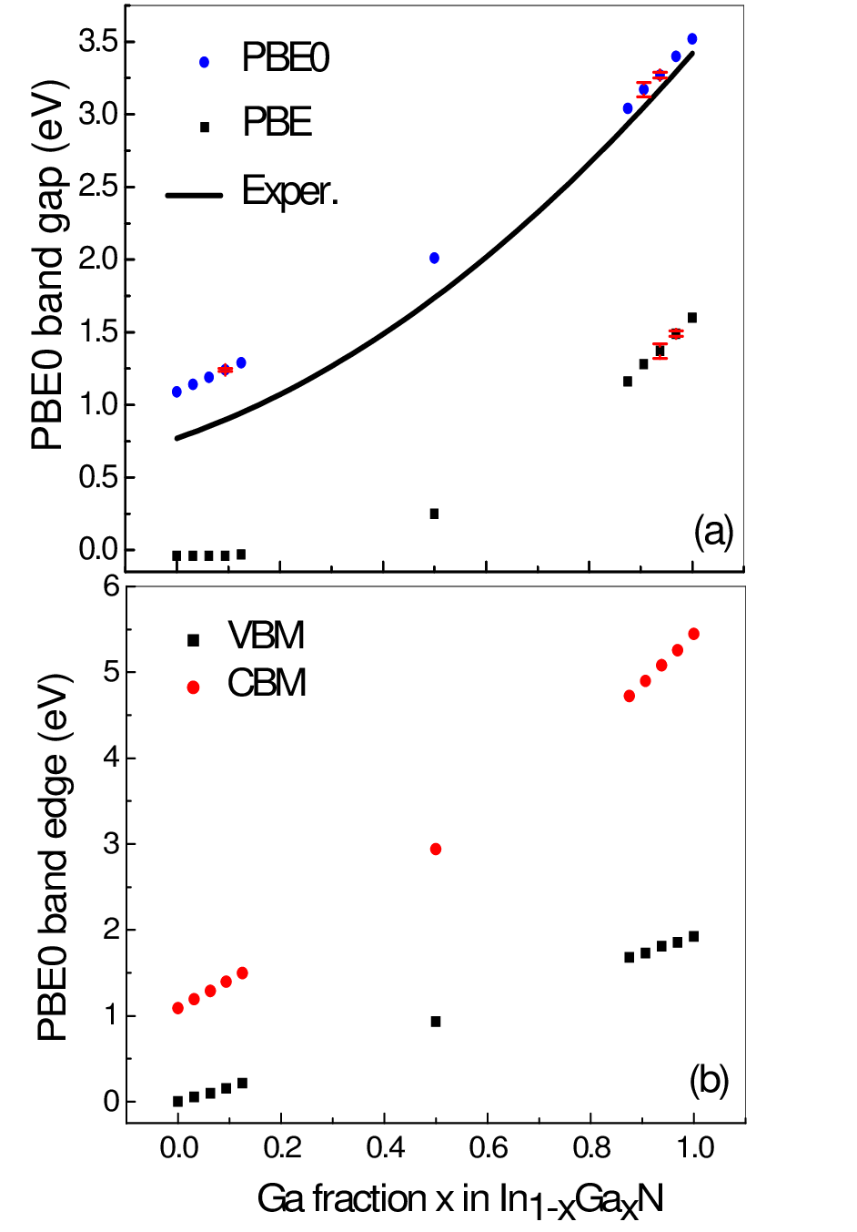
Besides confirming the good performance of hybrid functionals for band gap predictions, the above results for InN and GaN provide evidence of the reliability of our procedure for calculating the PBE0 band gap. We have thus applied this procedure to the study of the ternary In1-xGaxN compound, a system for which the standard reciprocal space approach to calculate the exact exchange would be extremely cumbersome. Instead, our order- scheme is well suited to treat systems for which large supercells are needed. Using a 64-atom supercell, we then considered In1-xGaxN models with 1(31), 2(30), 3(29), 4(28), 16(16), 28(4), 29(3), 30(2) and 31(1) Ga(In) cations, which correspond to = 0.031, 0.063, 0.094, 0.125, 0.5, 0.875, 0.906, 0.938, and 0.969. For each value of and a given configuration of Ga(In) atoms, the atomic positions were relaxed at the PBE level. The computed PBE0 band gap of In1-xGaxN as a function of the Ga fraction is shown in Fig. 2(a), together with experimental [31] and PBE results. We can see that PBE not only significantly underestimates the band gap but incorrectly shows a metallic ground state for . By contrast, a direct band gap at the point is found for all values of at the PBE0 level. Moreover, PBE0 predicts a large band gap bowing effect, in qualitative agreement with the experiment [31]. The band gap can be fitted to the quadratic form
| (9) |
from which a bowing coefficient = 1.63 eV can be extracted, similar to the value, 1.67 eV, found in previous screened-exchange density functional (-LDA) calculations [4]. However, this is somewhat larger than the experimental value = 1.43 eV [31], likely because of the overestimated PBE0 band gap for the In-rich compounds. To gain more insight into the origin of the large band gap bowing, we have examined how the valence band maximum (VBM) and conduction band minimum (CBM) depend separately on , see Fig. 3(a). In this analysis, the average electrostatic potential was taken as the reference for the band alignment. It can be seen that the VBM increases almost linearly with , whereas the CBM shows a stronger nonlinear increase which is responsible for the large bowing coefficient of the alloy.

The electronic states in proximity of the VBM are important for the pholuminescence properties of In1-xGaxN. These states have the character of orbitals localized at the N sites. Previous theoretical studies of In1-xGaxN found that in Ga-rich alloys the amplitude of these states is enhanced at N sites close to In impurities[4, 7], suggesting a localization of photoexcited holes at such sites. This interesting result is confirmed by our PBE0 hybrid calculations. The enhancement, or hole localization, is particularly evident when the In impurities are clustered to form a zigzag In-N-In-N-In chain, as shown in Fig. 3(a). This localization has been suggested to be the reason of the high efficiency of In1-xGaxN based emitting devices [4, 6]. Interestingly, we found that there is an opposite effect for the case of Ga impurities in In rich alloys. Here, a reduction of the states at the N sites along the Ga-N-Ga-N-Ga-N chain is observed, see Fig. 3(b).
In conclusion, we have described an efficient procedure to calculate the band gap of extended insulating systems using hybrid functionals. This procedure is based on the recently developed WSC order- method, in which the Hartree Fock exchange is calculated using MLWFs, and can therefore be used to study the band gap and other electronic properties of systems with large unit cells. We have demonstrated the effectiveness of our approach by a study of the band gap of a ternary compound, In1-xGaxN, that we have modeled using a 64-atom supercell. Hybrid functional results for this important material are here reported for the first time, without the approximation of screened exchange, and show a much better agreement with experiment than conventional DFT-GGA or LDA calculations. Our approach can be widely used for the band gap engineering problem in semiconductor alloys.
Acknowledgements.
This work has been supported by the Department Of Energy under grant DE-FG02-06ER-46344, grant DE-FG02-05ER46201 and by AFOSR-MURI F49620-03-1-0330. A. M. R. was supported by the (US) Department of Energy under grant DE-FG02-07ER46431References
- [1] P. Piquini, P. A. Graf, and A. Zunger, Phys. Rev. Lett. 100, 186403 (2008). S. V. Dudiy and A. Zunger, ibid 97, 046401 (2006).
- [2] A. Grüneis, K. Hummer, M. Marsman, and G. Kresse, Phys. Rev. B 78, 165103 (2008).
- [3] M. N. Huda, Y. Yan, S. -H. Wei, and M. M. Al-Jassim, Phys. Rev. B 78, 195204 (2008).
- [4] B. Lee and L. -W. Wang, J. Appl. Phys. 100, 093717 (2006).
- [5] J. W. Bennett, I. Grinberg, and A. M. Rappe, J. Am. Chem. Soc. 130, 17409 (2008).
- [6] S. F. Chichibu et al., Philos. Mag. 87, 2019 (2007).
- [7] L. Bellaiche, T. Mattila, L. -W. Wang, S. -H. Wei, and A. Zunger, Appl. Phys. Lett. 74, 1842(1999).
- [8] See e.g. R. G. Parr and W. Yang, Density Functional Theory of Atoms and Molecules (Oxford University Press, New York, 1989).
- [9] A. J. Cohen, P. Mori-S anchez, and W. Yang, Science 321, 792 (2008).
- [10] A. J. Cohen, P. Mori-S anchez, and W. Yang, Phys. Rev. B 77, 115123 (2008).
- [11] B. G. Janesko, T. M. Henderson, and G. E. Scuseria, Phys. Chem. Chem. Phys., 11, 443 (2009).
- [12] A. D. Becke, J. Chem. Phys. 98, 1372 (1993).
- [13] M. Marsman, J. Paier, A. Stroppa, and G. Kresse, J. Phys.: Condens. Matter 20, 064201 (2008).
- [14] X. Wu, A. Selloni, and R. Car, Phys. Rev. B 79, 085102 (2009).
- [15] N. Marzari and D. Vanderbilt, Phys. Rev. B 56, 12847 (1997).
- [16] J. P. Perdew, M. Ernzerhof, and K. Burke, J. Chem. Phys. 105, 9982 (1996).
- [17] J. P. Perdew, K. Burke, and M. Ernzerhof, Phys. Rev. Lett. 77, 3865 (1996).
- [18] N. Marzari and D. Vanderbilt, Phys. Rev. B 56, 12847 (1997).
- [19] R. Car, in Conceptual Foundations of Materials: A Standard Model for Ground- and Excited-State Properties, Contemporary Concepts of Condensed Matter Science, edited by S. G. Louie and M. L. Cohen (Elsevier, Amsterdam, 2006), Chap. 3, p. 64.
- [20] See http://www.quantum-espresso.org.
- [21] OPIUM pseudopotential package http://opium.sourceforge.net.
- [22] J. R. Trail and R. J. Needs, J. Chem. Phys. 122, 014112 (2005).
- [23] D. M. Bylander and L. Kleinman, Phys. Rev. Lett. 74, 3660 (1995); Phys. Rev. B 52, 14566 (1995); 54, 7891 (1996); 55, 9432 (1997).
- [24] M. Städele, J. A. Majewski, P. Vogl, and A. Görling, Phys. Rev. Lett. 79, 2089 (1997).
- [25] E. Engel, A. Höck, R. N. Schmid, R. M. Dreizler, and N. Chetty, Phys. Rev. B 64, 125111 (2001).
- [26] J. R. Trail and R. J. Needs, J. Chem. Phys. 122, 174109 (2005).
- [27] W. A. Al-Saidi, E. J. Walter, and A. M. Rappe, Phys. Rev. B 77, 075112 (2008).
- [28] A. M. Rappe, K. M. Rabe, E. Kaxiras, and J. D. Joannopoulos, Phys. Rev. B 41, R1227 (1990).
- [29] F. Fuchs, J. Furthmüller, F. Bechstedt, M. Shishkin, and G. Kresse, Phys. Rev. B 76, 115109 (2007).
- [30] L. F. J. Piper, T. D. Veal, P. H. Jefferson, C. F. McConville, F. Fuchs, J. Furthmüller,F. Bechstedt, H. Lu and W. J. Schaff, Phys. Rev. B 72, 245319 (2005).
- [31] J. Wu, W. Walukiewicz, K. M. Yu, J. W. Ager III, E. E. Haller, H. Lu, and W. J. Schaff, Appl. Phys. Lett. 80, 4741 (2002).