Gate tunable infrared phonon anomalies in bilayer graphene
Abstract
We observe a giant increase of the infrared intensity and a softening of the in-plane antisymmetric phonon mode ( 0.2 eV) in bilayer graphene as a function of the gate-induced doping. The phonon peak has a pronounced Fano-like asymmetry. We suggest that the intensity growth and the softening originate from the coupling of the phonon mode to the narrow electronic transition between parallel bands of the same character, while the asymmetry is due to the interaction with the continuum of transitions between the lowest hole and electron bands. The growth of the peak can be interpreted as a ”charged-phonon” effect observed previously in organic chain conductors and doped fullerenes, which can be tuned in graphene with the gate voltage.
There is a lot of interest in electronic properties of graphene, especially, due to the chiral nature of its quasiparticles [1]. Graphene also allows tuning the Fermi level continuously through zero energy by the ambipolar electric field effect, and this tunability has been intensively exploited in many experiments. In particular, it was found that electric field strongly affects electron-phonon interactions [2, 3, 4, 5, 6, 7, 8], which is hard or impossible to achieve in bulk materials. Particularly intriguing is the case of bilayer graphene, where the electric field breaks down the interlayer symmetry [1] and changes qualitatively the electron-phonon coupling [9]. Up to now the vast majority of the optical phonon studies in graphene were performed by Raman spectroscopy, whereas infrared techniques that can provide important complementary information, due to different selection rules, remain largely unexplored. Here we present an infrared study of the in-plane optical phonon mode in gated bilayer graphene. We observe several new phonon anomalies, of which the most spectacular one is a giant enhancement of the phonon resonance as a function of the gate voltage. In addition, the phonon peak is found to have a pronounced Fano shape [10], which indicates a coupling of this mode to a continuum of electron-hole excitations. We believe that this gate-tunable coupling can be used in various electro-optical applications.
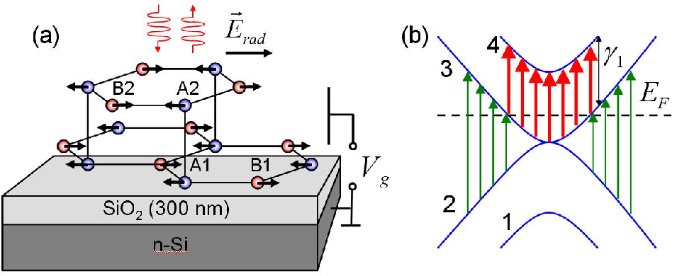
Reflectivity spectra of an exfoliated bottom-gated bilayer graphene flake on top of a SiO2(300 nm)/Si substrate (Fig.1a) were taken at 10 K at near-normal incidence using an infrared microscope attached to a Fourier transform spectrometer. Lithographically made leads allowed applying the gate voltage and measuring resistivity during the optical experiment. The charge neutral state corresponding to the resistivity maximum was observed at -30 V. Fig. 2a shows the reflectivity normalized to the bare substrate at various gate voltages from -100 V to 100 V. The doping level can be deduced using the relation [cm-2] = 7.21010 [V]. One can clearly see a phonon structure at about 1600 cm-1 (0.2 eV) corresponding to the infrared active antisymmetric mode (Fig.1a). In order to easier compare the phonon feature at different values of , in Fig.2b we subtract from the reflectivity curves a smooth baseline obtained by their low-order polynomial fitting outside the region 1500 - 1700 cm-1. While the structure is weak in the vicinity of , it grows quickly at elevated (both positive and negative) gate voltages.

It is not straightforward to interpret the phonon lineshapes in the raw reflectivity spectra, which are sensitive to the choice of the substrate. In Fig.3 we show the real part of the optical conductivity of graphene, , extracted using a Kramers-Kronig consistent variational spectra analysis [11] that takes into account the known optical constants and thicknesses of the SiO2 and Si layers. The smooth background due to direct optical absorption by electronic transitions, which is discussed in detail elsewhere [12, 13], is subtracted.
A few interesting observations can be made. First of all, the peak intensity grows rapidly as the gate voltage is tuned away from . Second, the phonon peak is clearly asymmetric, with a characteristic Fano lineshape [10] that is most pronounced at not very high values of (for example, at = -70, -80, 0, +10 V). Third, close to the charge neutral point (for example at -40 and -50 V), the peak is negative, i.e. the conductivity has a weak but a distinct dip. Fourth, the position of the peak maximum is gate-voltage dependent. For example, one can see that for V it shifts to lower frequencies as the gate voltage is increased.

The Fano lineshape provides evidence of a coupling between this sharp mode and a continuum of electronic excitations in the same energy range. Following the general Fano theory[10], the optical conductivity of such coupled system minus the background due to the bare continuum can described by the formula:
| (1) |
with . Here is the phonon frequency, is the linewidth and is the plasma frequency, which is proportional to the infrared effective charge as specified below. The asymmetry is described by a dimensionless parameter so that the symmetric Lorenzian lineshape is recovered in the limit . The doping dependence of the Fano parameters extracted by the fitting of the conductivity spectra of Fig.3 is shown in Fig.4a-d.

From Fig.4a one can see that decreases almost linearly with the slope -0.058 cm-1/V. Note that due to the Fano shape, is larger than the position of the conductivity peak maximum, the difference being dependent on the asymmetry parameter. This is why the softening is seemingly less pronounced in Fig.3b and 3c. The linewidth is enhanced at low doping levels and decreases with the increasing the gate voltage. The fitted value of shows a saturation at 10 cm-1, which is the resolution limit of this measurement and therefore an overestimation of the true linewidth. The plasma frequency is at minimum close to (Fig.4c), where cm-1 and strongly increases with the gate voltage. In Fig.4e we plot the bare phonon spectral weight as well as the peak area (integrated between 1570 and 1610 cm-1). Note that in the presence of coupling . If the asymmetry is very strong () then the area becomes negative. This is because is affected not only by the direct optical absorption due to the phonon mode but also by the coupling-induced transformations of the optical response of the continuum. In particular the negative value of is explained by the removal of spectral weight from the continuum. The asymmetry parameter also shows a strong doping dependence, with a decrease as the doping is increased. This decrease is not monotonic: the strongest changes are observed at 50 V, while at higher doping the asymmetry remains roughly constant.
Let us discuss the observed phonon anomalies and their relation to the band structure and electronic excitations. The frequency shift and the linewidth are related to the phonon self energy : , . The self energy for the zone-center optical phonons is given at zero temperature by a sum of the contributions of all vertical (momentum conserving) transitions across the Fermi level weighted with their respective electron-phonon matrix elements. Each contribution has a Lorentzian spectral shape , where is the transition energy and is a broadening parameter. Therefore is determined only by the transitions that overlap with the phonon energy within , while is affected by all transitions with non-zero electron-phonon matrix elements.
A simplified band structure of bilayer graphene, where we neglect the electron-hole asymmetry and the bandgap, is shown in Fig.1b. Each of the hole and electron bands is split into two parallel subbands (numbered 1,2 and 3,4 respectively) separated by the interplane hopping energy 0.4 eV. We shall refer to the case of electron doping (positive gate voltages) although the results are equally valid for hole doping. Based on this band structure, Ando calculated the phonon self energy and predicted the softening of the phonon with doping [7], in an excellent agreement with the present infrared measurement. Interestingly, the softening was also found in a Raman study [4], where the mode was observable due to a possible breaking of the inversion symmetry of bilayer graphene in the used device. By comparing the observed slope with the theoretical curve we estimate the dimensionless electron-phonon coupling parameter defined in Ref.7 to be about , in agreement with the Raman study [4]. According to Ando [7], the softening of the mode is due to the contribution to the self energy coming from the transitions between the bands 3 and 4 (thick red arrows in Fig.1b). Since the two bands are parallel, these transitions form a narrow peak centered at . Its intensity grows rapidly with doping in the course of the progressive filling of the band 3.
It is important that none of the interband transitions, except the ones between the bands 2 and 3, overlap with the phonon energy, as is about twice as large as . On the other hand, the electron-phonon matrix elements between the mode and the excitations vanish according to the symmetry analysis [7]. Therefore, the same calculation [7] predicts a very small and weakly doping dependent linewidth of the phonon mode. Instead, we observe that is large ( 20-30 cm-1) at low doping and strongly decreases with (Fig.4b).
We argue that the large linewidth and the Fano shape of the phonon peak are likely due to the interaction with the transitions (shown with thin green arrows in Fig.1b), despite the fact that the self-energy calculation Ref.[7] would suggest a negligible coupling in this case.
The transitions form a continuum of particle-hole excitations. Such a continuum is also present in monolayer graphene and in graphite, where it results in the universal optical conductivity of [14, 15, 16, 17]. The continuum starts at due to the Pauli principle [14]. If then the phonon frequency lies inside the continuum and in this case one expects the linewidth and the asymmetry to be stronger. Indeed, we see a clear correlation between the sudden decrease of the asymmetry parameter (Fig.4d), the decrease of the broadening (Fig.4b) and the reduction of the background electronic optical conductivity at the phonon frequency (Fig.4e) [13], which corresponds to . It is worth mentioning that the anomalous softening of the Raman-active phonon mode in bilayer graphene is observed at about the same gate voltage [3].
Among the possible reasons of the ”forbidden” interaction between the mode and the electronic excitations we can mention (i) the electron-hole asymmetry, which is clearly observed in the electronic infrared spectra [18, 19, 12, 13] and (ii) an electric field generated by the gate electrode and charged impurities which breaks the inversion symmetry [9]. Note that a Fano phonon lineshape in the infrared spectra of bilayer graphene was also observed in Ref.[20].
Finally, we discuss the most spectacular effect of this study: a large increase of the phonon intensity as a function of doping. From the plasma frequency we can deduce the dimensionless effective infrared charge of the mode , where is the number of atoms in the unit cell, is the unit cell volume, is the mass of the carbon atom and is the elementary charge. The doping dependence of the effective charge is shown in Fig.4c. One can see that at high gate voltages exceeds 1, which is the value observed in entirely ionic compounds like NaCl and LiF. We first compare this value to the effective charge of the static dipole created because the doped charge is distributed not equally between the atomic positions A1(A2) and B1(B2) (Fig.1a). The static charge calculated using the tight-binding model (the dashed line in Fig.4c) appears to be more than 300 times smaller than the observed infrared (dynamical) effective charge. Such an utter discrepancy calls for a radically different physical approach.
Notably, similar effects of a large enhancement of vibrational resonances were observed in organic linear-chain conductors such as K-TCNQ [21] and in doped C60 [22]. Effective infrared charges significantly larger than ionic charges were also found in some transition metal compounds, for example in FeSi [23]. These findings were explained using the so-called ”charged-phonon” theory of M.J.Rice et al. [24]. Within this model, the molecular vibrations that are usually not active or weakly active in the infrared range become enhanced due to a coupling to electronic resonances at higher energy (such as the transition in doped ). Their effective charge is effectively ”borrowed” from the electronic transitions, in accordance with the f-sum rule.
A clear correlation between the intensity of the phonon resonance and the strength of the electronic transition was experimentally observed [22]. The charged-phonon model thus seems to be relevant to the intensity enhancement of the mode in bilayer graphene, in view of the observation that the strong doping dependence of the intensity of the 34 transition correlates with the growth of the phonon peak. Interestingly, a simultaneous increase of the phonon intensity and electronic absorption with doping was also found in organic field effect transistors [25]. We note that even at zero doping, where the intensity of the transition is zero, the effective charge is about 0.25. This suggests that other transitions (, and ), which remain populated at all doping levels, also contribute to . We notice that the zero-doping value of is comparable with the ones reported in graphite [26].
As a concluding remark, the possibility to control the phonon intensity by the gate voltage might be of practical importance, for example, in optoelectronics. We also suggest that the peak can be used as a doping indicator.
In summary, we observed several anomalies of the infrared active mode in bilayer graphene: (i) a drastic intensity enhancement and a softening as a function of doping, (ii) a strong Fano-like asymmetry of the lineshape, with even a negative peak area at low doping. We suggest that the coupling to the narrow transition is responsible for the mode softening [7] and the intensity enhancement, via the charged-phonon mechanism [24]. The interaction with the continuum likely gives rise to the asymmetry and the broadening of the phonon peak. Further studies are required to understand quantitatively the complicated picture of the electron-phonon coupling in graphene. This work was supported by the Swiss National Science Foundation (SNSF) by the grant 200021-120347, through the National Center of Competence in Research ”Materials with Novel Electronic Properties-MaNEP” and by Italian MIUR project PRIN 2007FW3MJX.
References
- [1] See for review, A. H. Castro Neto et al., Rev. Mod. Phys. 81, 109 (2009) and references therein.
- [2] S. Pisana et al., Nature Mater. 6, 198 (2007).
- [3] J. Yan, E. A. Henriksen, Ph. Kim and A. Pinczuk, Phys. Rev. Lett. 101, 136804 (2008).
- [4] L. M. Malard, D. C. Elias, E. S. Alves, and M. A. Pimenta, Phys. Rev. Lett. 101, 257401 (2008).
- [5] T. Ando, J. Phys. Soc. Japan 75, 124701 (2006).
- [6] A.H. Castro Neto and F. Guinea, Phys. Rev. B 75, 045404 (2007).
- [7] T. Ando, J. Phys. Soc. Japan 76, 104711 (2007).
- [8] J.-A. Yan, W. Y. Ruan, and M.Y. Chou, Phys. Rev. B 79, 115443 (2009).
- [9] T. Ando and M. Koshino, J. Phys. Soc. Japan 78, 034709 (2009).
- [10] U. Fano, Phys. Rev. 124, 1866 (1961).
- [11] A.B. Kuzmenko, Rev. Sci. Instrum. 76, 083108 (2005).
- [12] A. B. Kuzmenko et al., Phys. Rev. B 79, 115441 (2009).
- [13] A.B. Kuzmenko et al., arXiv:0908.0672, to be published.
- [14] T. Ando, Y. Zheng, H. Suzuura, J. Phys. Soc. Japan 71, 1318 (2002).
- [15] A. B. Kuzmenko, E. van Heumen, F. Carbone, D. van der Marel, Phys. Rev. Lett. 100, 117401 (2008).
- [16] R.R. Nair et al., Science 320, 1308 (2008).
- [17] Z.Q. Li et al., Nature Physics 4, 532 (2008).
- [18] L. M. Zhang et al., Phys. Rev. B 78, 235408 (2008).
- [19] Z.Q. Li et al., Phys. Rev. Lett. 102, 037403 (2009).
- [20] Y. Zhang, Nature 459, 820 (2009).
- [21] D.B. Tanner, C.S. Jacobsen, A.A. Bright, and A.J. Heeger, Phys. Rev. B 16, 3283 (1977); G.R. Anderson and J.P. Devlin, J. Phys. Chem. 79, 1100 (1975);
- [22] K.-J. Fu et al. Phys. Rev. B 46, 1937 (1992).
- [23] A. Damascelli, K. Schulte, D. van der Marel, and A. A. Menovsky, Rev. Rev. B 55, R4863 (1997).
- [24] M.J. Rice, N.O. Lipari and S. Strassler, Phys. Rev. Lett., 39, 1359 (1977); M. J. Rice and H.-Y. Choi, Phys. Rev. B 45, 10173 (1992).
- [25] Z.Q. Li et al., Nano Letters 6, 224 (2006).
- [26] R. J. Nemanich, G. Lucovsky, and S. A. Solin, Solid State Commun. 23, 117 (1977); S. Leung, C. Underhill, G. Dresselhaus, and M. S. Dresselhaus, Solid State Commun. 33, 285 (1980).