Theory of optical conductivity for dilute
Abstract
We construct a semi-microscopic theory, to describe the optical conductivity of in the dilute limit, . We construct an effective Hamiltonian that captures inside-impurity band optical transitions as well as transitions between the valence band and the impurity band. All parameters of the Hamiltonian are computed from microscopic variational calculations. We find a metal-insulator transition within the impurity band in the concentration range, for uncompensated and for compensated samples, in good agreement with the experiments. We find an optical mass , which is almost independent of the impurity concentration excepting in the vicinity of the metal-insulator transition, where it reaches values as large as . We also reproduce a mid-infrared peak at , which redshifts upon doping, in quantitative agreement with the experiments.
pacs
75.50.Pp, 78.66.Fd, 78.66.Fd, 78.20.-e, 78.67.-n.I Introduction
The diluted magnetic semiconductor (DMS) Ga1-xMnxAs has emerged as one of the most promising materials due to its potential applications in spin-based technology. This material is, however, equally interesting from the point of view of fundamental research for its unique properties and the rich physics it displays; is a strongly disordered ferromagnet, where the interplay of ferromagnetism, localization, magnetic fluctuations and the presence of strong spin-orbit coupling lead to many interesting properties such as a strong magnetoresistance,[1, 2] resistivity anomalies,[2, 3, 4, 5] or the presence of a large anomalous Hall effect.[6]
Although has been the subject of intense theoretical and experimental investigation, even its most basic properties are still debated. One of these fundamental and unresolved issues is the existence or non-existence of an impurity band in this material. There is a general consensus that for very small magnetic concentrations, , is described in terms of an impurity band. For higher concentrations, however, there is no general consensus yet: On one hand, essentially all spectroscopic measurements such as ARPES,[7] STM,[8] optical conductivity data,[9, 10, 11, 12] and ellipsometry [13] seem to favor the presence of an impurity band even up to moderate concentrations (), and even high quality samples with a high Curie temperature and a clearly metallic behavior have surprisingly small values of .[2, 12] On the other hand, many properties of these materials can be even quantitatively understood in terms of a disordered valence band picture, and, in fact, from a theoretical point of view, it is hard to understand how an impurity band could survive up to concentrations as high as .[14]
In the present paper we shall not attempt to resolve this discussion, rather, we would like to focus exclusively on the optical conductivity. Typical optical conductivity measurements in display two rather remarkable features: a mid infrared resonance peak at approximately that redshifts with increasing hole concentration, ; a large optical mass of the order , implying a mobility which is orders of magnitude smaller than the one of doped with similar concentrations of non-magnetic impurities.[15]
In this paper we aim at developing a semi-microscopic theory for the optical conductivity of in the very dilute limit, . There are several theoretical studies of the optical conductivity of by now.[16, 17, 18, 19, 20] Maybe the most realistic calculations have been carried out in Refs.[16] and [17], however, the results of these works are somewhat conflicting: In Ref. [16] a disordered valence band described in terms of the Luttinger model has been studied. In these calculations, rather surprisingly, the mid-infrared peak appeared even in a simplified parabolic model, where a completely isotropical valence band mass was assumed and the spin-orbit split valence band is completely ignored. Therefore the authors concluded that the mid-infrared peak is not due to transitions to the spin-orbit split valence band, rather, they interpreted it as a result of strong localization and interference effects. In another, very thorough calculation[17], realistic tight binding models have been used, but the results were conflicting in that features associated with an impurity band have or have not appeared depending on the particular tight binding scheme applied.
Unfortunately, none of these previously applied methods is appropriate to study accurately the dilute limit, . This small concentration limit is of particular interest, since the metal-insulator transition takes place at concentrations as low as ,[21] and furthermore, it is in this limit where features associated with the impurity band should be present. In the present paper, we shall follow the lines of Ref. [22] and develop a semi-microscopical approach to capture the physics of this dilute limit. At the microscopic level, we describe the valence band holes as spin carriers, which interact with the external electromagnetic vector potential and the Mn ions, as described by the following Hamiltonian:
| (1) | |||||
Here and () denote the valence hole coordinates and momenta, and the Mn atoms are located at random positions, (). In the first term we assume an isotropic effective mass . This is a somewhat uncontrolled approximation. However, according to the results of Ref. [16], inclusion of a more realistic band structure influences only slightly the optical spectrum for frequencies , we shall therefore ignore it here. The second term describes the random potential created by the Mn atoms, and it incorporates the Coulomb attraction as well as the central cell correction.[23] Finally, the last term describes the local exchange interaction between the manganese magnetic moments, and the spin of hole , . The parameters of the ’microscopic’ Hamiltonian Eq. (1) are all well-known.[24]
In our work we use the Hamiltonian (1) as a starting point, and derive a microscopic effective Hamiltonian from it that captures the impurity band physics in the very dilute limit, but also accounts for impurity band-valence band transitions (for details see Section II). This effective Hamiltonian can then be used to compute the optical conductivity using field theoretical methods, as detailed in Section III. With this ’multiscale approach’, we are then able to determine the optical properties of accurately in the small concentration regime, while keeping .

One of the key elements of our approach is the assumption that, for these small concentrations, the Fermi level lies inside the impurity band. This is indeed evidenced by transport measurements,[21] which clearly show that the activation energy (associated with localized impurity states to valence band transitions) remains finite as one approaches the metal insulator transition.[21] This implies that the metal-insulator transition takes place within the impurity band, and one must be able to capture the properties of small concentration metallic samples using our impurity band-based method.
Indeed, our results also support this picture; a detailed analysis of the hole states reveals a metal-insulator transition at about , where delocalized states appear in the middle of the impurity band. As shown in Fig. 1, this is approximately the critical concentration for uncompensated samples. The Anderson transition thus takes place inside the impurity band, in agreement with the conclusions of Ref. 22, and also in good agreement with activation energy values observed for samples grown at high temperature.[25, 26] Typically, however, samples grown under non-equilibrium conditions are compensated even after annealing: in addition to the substitutional Mn ions (of concentration ) there is also a finite concentration of interstitial Mn ions, which behave as double donors, and are also believed to make a fraction of the Mn ions inactive by simply binding to them.[27] As a result, the effective concentration of “active” Mn ions is reduced to and the concentration of holes is also suppressed compared to by the hole fraction . Remarkably, even if only 20 of the Mn ions goes to interstitial positions, that reduces the effective concentration to 60 percent of the total Mn concentration and amounts in a hole fraction . Unannealed samples tend to have even larger interstitial Mn concentrations and thus much smaller hole fractions.[27, 28, 24] As a result, depending on the precise annealing protocol, ferromagnetic samples (grown under non-equilibrium conditions) tend to show the phase transition at higher concentrations. According to our calculations, for () the metal insulator transition takes place at about , while for () the transition occurs at . These values are consistent with the experimental data.[29, 25, 30, 31, 32] In the rest of the paper, we shall not make a difference between substitutional and interstitial Mn ions, rather, by the symbol we shall refer to the concentration of active / effective Mn ions, which participate in the formation of the ferromagnetic state, and will be the corresponding hole fraction.
We also find that the optical mass increases to very large values at the critical concentration, where the DC conductance vanishes. However, apart from this, the optical spectrum changes rather continuously. For larger Mn concentrations, , we obtain an optical mass , which is almost independent of the hole concentration , and is in surprisingly good agreement with the experimental values.[11]
Our approach is designed to work in the limit of small concentrations, and it should break down for large concentrations. Where exactly this breakdown takes place, is not quite clear. Our calculations show that the impurity band is not merged with the valence band for concentrations as large as . Furthermore, the impurity band picture may make sense for even larger concentrations if the Fermi level is inside the gap (as indicated by ARPES measurements),[7] where states are expected to exhibit a stronger impurity state character. We are not able to convincingly determine the upper limit of our approach. However, if we blindly extend it to the regime , without justifying their applicability, rather surprisingly, our calculations qualitatively as well as quantitatively reproduce all important features of the experiments.

One of the typical optical conductivity results is displayed in Fig. 2, where, for comparison, we also show some typical experimental data.[11] In our calculations the Drude contribution originates entirely from carriers residing within the impurity band, and the ’Drude peak’ appears as a plateau at smaller frequencies, just as in the optical conductivity experiments. The mid-infrared peak, on the other hand, is due to transitions from the impurity to the valence band. Notice that the position as well as the overall size of the signal are quantitatively reproduced.
Having the Fermi level within the impurity band naturally explains the redshift of this resonance with increasing hole concentration. In Fig. 3 we show the computed peak position as a function of the effective optical spectral weight, (defined through Eq. (28)) for a variety of concentrations and hole fractions, . Our calculations show excellent agreement with the experimental results of Ref. 11.

The paper is organized as follows. First, in Section II we outline the calculations that lead from the microscopic Hamiltonian Eq. (1) to the effective Hamiltonians used. Some of the details of these rather technical variational calculations are given in appendices A and B. Sec. III provides the basic expressions for the optical conductivity within a mean field approach, while the results of our numerical calculations are given in Sec. IV. In Sec. V we show how to incorporate the effects of magnetic fluctuations, and finally, we conclude in Sec. VI.
II Theoretical framework
With current day computer technology, it is essentially impossible to treat the Hamiltonian of Eq. (1) accurately for small Mn concentrations, . We therefore describe this regime in terms of an effective Hamiltonian, which we derive from Eq. (1), and which consists of an impurity band part and a valence band part. The first part of the present Section focusses on this mapping. However, to compute the optical conductivity, we also need to determine how the electromagnetic field in Eq. (1) couples to impurity states within the effective Hamiltonian. This is discussed in the second part of the Section. In the main body of the text we only outline and summarize the most important steps. Details on these simple but rather lengthy calculations are given in Appendices A-B, and are provided as supplementary information.
II.1 Effective Hamiltonian
II.1.1 Impurity band Hamiltonian
Since for very small concentrations the Fermi energy is in the impurity band, we first need to describe the impurity states. In the small concentration limit, hole wave functions are localized at the Mn sites, providing a strong and attractive potential for them. Therefore the impurity band can be described using a tight binding Hamiltonian of the form,[33, 22]
| (2) | |||||
Here creates a bound hole at Mn position in a spin state , and denotes the hopping between Mn sites and . Since the hole mass is isotropic in our microscopic Hamiltonian, the hopping is independent of the hole spin . 11 1 A careful calculation using the full six band Hamiltonian shows that the hopping is indeed fairly isotropic as long as the hopping distance is less than about .[34] The on-site energy contains the binding energy of the hole, , but it also accounts for the Coulomb and kinetic energy shifts generated by neighboring Mn ions. Finally, the last term describes the local antiferromagnetic exchange with the core Mn spin .
The parameters appearing in Eq. (2) can be determined from experiments and from the microscopic Hamiltonian, Eq. (1). The coupling is known from EPR experiments to be for a single Mn impurity.[35, 13] However, the hopping parameters and the on site energy, need to be computed from Eq. (1). Similar to Ref. 22, we determined them from a variational calculation of the molecular orbitals for an Mn2 ’molecule’, described by the Hamiltonian:
| (3) |
where we used atomic units, , is the dielectric constant of , and . The so-called central cell correction accounts for the local interaction at the Mn core, and is given by[36]
| (4) |
The parameters and must be chosen to reproduce the experimentally observed impurity state at . In our calculations we have used and , but our results do not depend on this particular choice as long as is sufficiently small. Details of this variational calculation are presented in Appendix B). In these calculations we neglected the coupling , since it is much smaller than the binding energy of the holes. The final result is that (for ) the low lying spectrum of two Mn ions at a separation can be described by the following simple effective Hamiltonian,
| (5) |
The parameters and are shown in Fig. 4. As the inset of the lower panel of Fig. 4 shows, much of the energy shift originates from a simple long-ranged Coulomb shift due to the Coulomb potential of the neighboring Mn site, . The remaining kinetic shift, is relatively large for small separations, but vanishes exponentially for large values of .


Having determined the spectrum and the effective Hamiltonian of the two-Mn ion complex, we can now express the parameters of the effective Hamiltonian, Eq. (2). The hopping parameter between sites and depends just on their separation, , and is simply , the hopping obtained from the two-Mn problem, while the on-site energies in Eq. (2) are given as
| (6) |
The sum in this equation should be evaluated carefully: As we discussed above, for large separations, the shifts are dominated by the long-range Coulomb contributions, and therefore the sum in Eq. (6) formally diverges. This Coulomb potential is, however, screened by the bound valence holes and other charged impurities in the system, with a screening length of the order of the typical Mn-Mn distance. Therefore we shall compute the sum in Eq. (6) with an exponential cut-off, , , with ( the Mn concentration).
Also, our calculation for the hopping matrix elements makes sense only for nearest neighbor sites. Correspondingly, in the Hopping part of the Hamiltonian we introduce a rigid cut-off, , to keep only hopping to the first ’shell’ of atoms. Our results do not depend too much on these cut-off parameters; Changing the Coulomb energy cut-off results in an overall shift of the impurity and valence band energies, and does not influence the optical spectrum. Similarly, the results are almost independent of as long as it is in the range of, .
II.1.2 Valence band
In the tight-binding approach of the previous subsection only the bound hole states appear. However, to describe optical transitions, we also need to account for extended states within the valence band. These states are involved in local optical transitions, where a hole localized at site absorbs a relatively high energy photon () to make a transition relatively deep into the valence band.
To account quantitatively for these transitions, we make the following crucial observations: (i) The transitions involve hole states of relatively high energy, and correspondingly, states of a relatively short wavelength. (ii) Since the initial hole states are localized at the Mn site, the created valence band hole will also be localized close to it. There the major effect of neighboring Mn sites is to create a Coulomb potential, which is smooth at the scale of the wavelength of the created hole. As a result, we can describe the final hole state in terms of the following simplified ’semiclassical’ Hamiltonian:
| (7) |
where is the electron coordinate measured from impurity , and the shift is given by
| (8) |
Notice that since most of shift comes from the Coulomb shift in Eq. (6) (see Fig. 4). However, these two energies are not exactly the same, , since also contains the kinetic shift , shown in the inset in Fig. 4. It is precisely this kinetic shift, which is responsible for the red-shift of the mid-infrared optical peak with increasing Mn concentrations, .
Furthermore, we observe that local optical transitions only involve -states. These states vanish at the origin, and do not really feel the central cell correction. Therefore, to describe the local optical transitions, it is reasonable to include locally these -states only, and describe the valence band in a second quantized formalism as
| (9) |
where creates a scattering state in the -channel around impurity site in angular momentum channel , with spin (), and radial momentum . The operators are normalized to satisfy the anticommutation relation
| (10) |
As mentioned above, scattering states in the -channel do not feel the central cell correction, therefore the ’s create to a very good approximation Coulomb scattering states. Notice that in Eq. (9) an independent local band is associated with each impurity site, i.e., propagation between various impurity sites within the valence band is ignored. This is a reasonable approximation for the high-energy, fast processes considered in this work.
II.2 Coupling to the electromagnetic field

At the microscopic level, the vector potential couples directly to the momenta of the valence holes. However, within the impurity band, these valence holes reside on specific orbitals localized at the Mn sites, and therefore, as a first step, we need to determine how the vector potential couples to these impurity band states. To this end, we determined the matrix elements of the momentum operator between the lowest lying states of our Mn2 molecule (see Appendix B). We find that the effective coupling of a homogeneous vector potential to the impurity band is given by
| (11) |
where the unit vector specifies the direction of the bond, and is the momentum matrix element extracted from the variational calculation. This matrix element is plotted in Fig. 5. As we also verified, for , this tediously-obtained matrix element is quite well-approximated by the simple Peierls substitution,
| (12) |
The term (11) describes intraband transitions between states inside the impurity band. It is this term that generates the Drude peak and which is responsible for the AC conductance.

However, we also need to account for interband transitions, i.e. transitions from the impurity band to extended states in the valence band. In our approach, these transitions are local, and are described by the Hamiltonian,
| (13) |
Here denote the components of the vector potential , and the on-site optical matrix elements can be computed from the variational wave function of a single Mn site, We determined for Coulomb scattering states as well as for free electron states (details of this calculation are presented in Appendix A ). The final results are shown in Fig. 6.
For free-electron scattering states the single-parameter matrix element takes on a particularly simple form,
| (14) |
where . The momentum matrix elements vanish for since -states have a node at the origin, but they also vanish for very large momenta, where the valence hole wave functions oscillate much faster than the characteristic scale of the bound state. This results in a maximum optical transition rate for valence states at about below the valence band edge. It is this momentum-dependence of the optical matrix element that is ultimately responsible for the mid-infrared peak in the optical spectrum at frequencies . The Coulomb and free electron matrix elements behave qualitatively the same way and are in both cases well approximated by the expression obtained for a single hydrogen-like variational wave function, . However, the more realistic Coulomb matrix elements have a somewhat smaller amplitude and the maximum transition rate occurs at slightly higher values. In the rest of this paper we shall use these more realistic Coulomb matrix elements to compute the optical conductivity.
III Optical conductivity at : Mean field approximation
In the rest of the paper we shall focus on the calculation of the optical properties of at low temperatures. First, we shall discuss the case of temperature and treat the Mn spins within the mean field approximation, justified by the relatively large value of the Mn spins, . Later in section V we shall discuss how one can go beyond this approximation and compute spin wave corrections. These corrections, however, turn out to be small, and the mean field description turns out to be quite accurate. This is related to the fact that, in the concentration range studied here, the coupling is much smaller than the binding energy of the holes as well as the width of the impurity band, and therefore it hardly influences the optical spectrum at these energies.
III.1 Mean field Hamiltonian
In our model Hamiltonian, Mn spins couple directly only to states in the impurity band. Therefore, as a first step, we only need to treat the coupled Mn spin-impurity band system, described by Eq. (2). At the mean field level, the interaction part is rewritten as
| (15) | |||||
| (16) |
and the fluctuating part, is neglected. With this approximation, Eq. (2) becomes exactly solvable at any temperature. For given values of , the hole part of the Hamiltonian is diagonalized by the unitary transformation
| (17) |
where wave functions can be found by solving a relatively simple eigenvalue equation. The mean field Hamiltonian can then be rewritten in terms of the operators and the corresponding eigenenergies, , as
| (18) |
where the local fields can be expressed in terms of the new basis as
| (19) | |||||
| (20) |
with the Fermi function. Trivially, determines the expectation value , that enters the eigenvalue equation of . This field must therefore be determined selfconsistently. At temperature the selfconsistency equations become rather simple, since then the spins are completely polarized in the direction , , and the Fermi function simply becomes a step function. However, for small concentrations and/or finite temperature the Mn spins are not fully polarized, and the numerical solution of the mean field equations becomes time-consuming.
III.2 Optical conductivity
The mean field solution of the Hamiltonian provides us the equilibrium state of the coupled spin-impurity band system. To compute the optical spectrum, however, we also need to transform the coupling to the electromagnetic field to the ’canonical’ basis, Eq. (17).
We can express the coupling of the impurity band to a time-dependent vector potential in terms of the canonical operators, as , where the current operator’s matrix element is defined as
| (21) |
Similarly, we rewrite the term (13) in the Hamiltonian in this canonical basis as
| (22) |
with .
The optical conductivity can be computed by means of the Kubo formula, which expresses it in terms of the retarded current-current correlation function,
| (23) |
Since, corresponding to Eqs. (21) and Eq. (22), our current operator consists of an interband and an intraband part, the current-current correlation function can also be expressed in terms of two contributions: an intraband contribution, , corresponding to transitions within the impurity band, and an interband contribution, , describing transitions from the impurity band to the valence band. In our approach the low frequency behavior arises from impurity band scattering alone, while the valence band plays practically no role there. The high frequency conductivity, on the other hand, is typically dominated by interband transitions to the valence band. In the present, impurity band approach, these transitions give rise to a mid-infrared peak close to .
The previously mentioned two contributions can be easily computed within the mean field approach, using the diagrammatic formalism presented in Section V, and the interband contribution can be simply expressed as
| (24) |
Notice that the transition being local, it is also the local energy of a valence band hole, that appears in the denominator of this expression, .
The intraband contribution can be written in a similar way as
| (25) |
with the polarization of the external light.
Clearly, both the energy and the precise structure (i.e., localized or extended character) of the impurity band states enter the matrix elements in the above expressions. However, apart from the value of the DC conductance, which clearly must vanish as one approaches the localization transition, the gross high-frequency features will turn out to not be very sensitive to the localization transition itself. This is not very surprising, since the localization transition involves mostly states at the Fermi energy, while optical transitions are dominated by states deep below or high above the Fermi energy.
IV Mean field results
IV.1 Density of states


Let us start first by discussing some details of the numerical solution of the mean field equations described in the previous section, and the structure of the hole states obtained. To start the numerical calculation, we first generate an initial distribution for the substitutional impurities on an fcc lattice with lattice constant . Nearest neighbor Mn sites are, however, not favored during the growth process, since Mn ions act as charged impurities. To simulate this effect, we let the Mn ions relax through a simple classical Monte Carlo diffusion process while assuming a screened Coulomb interactions between them.[22] Typical values of this Monte Carlo time used are in the range of . In all our calculations we use periodic boundary conditions to suppress surface effects.
Once the configuration of the ions is determined, we can construct the effective Hamiltonians Eq. (2) and (9) as described in Section II.1, Having constructed the Hamiltonian, we then solve the mean field equations iteratively and determine the equilibrium spin configuration. Here we only focus on temperature, where , with acting simply as a classical variable. In the end of the mean field self-consistency loop the states in the impurity and valence band are fully characterized, i.e. the corresponding eigen-energies and as well as the wave functions are available. We can then compute the necessary matrix elements of the current operator using Eq. (11), and apply (23) and (38) immediately to compute the contributions to the optical conductivity.
For a good accuracy, we consider system sizes as large as possible, and we average over many configurations. Usually for a given concentration and hole fraction, we average over 100 different impurity configurations, and we consider systems with the number of impurities in the range of 200.
In Fig. 7 we present results for the impurity band density of states (DOS) for different concentrations but for a fixed hole fraction, . We also indicate the average DOS for the valence band. Shaded regions, denoting localized states were determined by by analyzing the finite size scaling of the participation ratio
| (26) |
For extended states scales with the system size, while for the localized states remains finite for . Fig. 8 shows the details of such a finite size scaling analysis.
As we expect, increasing the concentration, the impurity band gets broader and starts to overlap with the valence band for concentration as low as 0.5% (see also Fig.7). However, at the same time increasing Coulomb disorder shifts the tail of the impurity band deeper inside the gap (the top of the valence band is fixed at ). States inside this tail are strongly localized and have an overwhelming localized impurity state character.
We clearly observe a metal insulator transition (MIT) at a critical concentration %, which corresponds to a hole concentration for . In our approach this metal-insulator transition is simply an Anderson localization transition, since electron-electron interaction effects are neglected: For % all the states in the impurity band are localized by disorder and the system is an insulator, while for % the metallicity of the system still depends on the position of the Fermi level inside the impurity band. As an example (see Fig.8, bottom layer) for and hole fractions less than the system is still an insulator, while for a hole fraction , the Fermi level is already inside the delocalized region and we find a metallic state. Increasing the concentration to larger values, the extended region grows and the system has a metallic behavior for typical values of the hole fraction, , (see also Fig. 7). For hole fractions , e.g., we find that the ground state is metallic for . These numbers are in very good agreement with experimental results, where the MIT has been reported to occur in a concentration range %.[14, 26]
We must remark that here we completely neglected electron-electron interaction. Electron-electron interaction can obviously modify many of the physical properties close to the MIT and lead to the appearance of a Coulomb gap as well as Altshuler-Aronov-type anomalies.[37] On the other hand, even annealed samples are typically compensated, and the electron-electron interaction has been found to be less relevant for such systems. Also, we can argue that our results are in a way self-consistent, and probably not very sensitive to Coulomb interaction; For typical concentrations and hole fractions in the range , we find that aproximately of the sites have less then one electrons on them, and less then of sites are more then doubly occupied. Furthermore, even for the most localized orbitals, the participation ratio is rather large . Therefore, a typical site is occupied by a single electron and the Coulomb correlations are not too relevant.[22] Treating the Coulomb interaction appropriately is, however, a real theoretical challenge even for much simpler model systems, and is beyond the scope of the present work.

Let us close this subsection by presenting a rather curious quantity that we termed ’shifted local density of states’ (shifted-LDOS), where at every site we computed the local density of states by subtracting the binding energy of a hole, , as well as the value of the average Coulomb shift. While the unshifted LDOS is rather featureless, this quantity displays a sharp peak around zero energy. A more detailed analysis reveals that this sharp peak is associated with localized states having a small participation ratio, i.e. states in the tail of the impurity band. To show this, we also plotted the contribution of states with ’s smaller than a given value to the shifted-DOS. Clearly, the peak observed at zero energy is entirely due to localized states deep inside the gap. The physical interpretation of this peak is thus plausible; States in the tail of the impurity band are generated by random and large fluctuations of the Coulomb disorder. These states are simply localized impurity states deep inside the gap that are being mostly occupied, and they give rise to local optical transitions which have a strong impurity state transition character.
IV.2 Optical conductivity

Having diagonalized the mean field Hamiltonian, it is straightforward to compute the optical conductivity. As we shall see, our theory, which incorporates inter-impurity band transitions as well as intraband transitions, accounts qualitatively as well as quantitatively for all major features of the experimentally observed optical spectrum. We shall also present a scaling analysis of the optical conductivity close to the metal-insulator transition and compute the dynamical critical exponent.
The Drude contribution, i.e. the feature is controlled by excitations close to the Fermi level. Since in this small concentration limit the Fermi level resides in the impurity band, the “Drude peak” and also the DC conductivity are expected to be dominated by the intra impurity band contribution. The contributions of extended valence band states is negligible for , since these states are too far from the Fermi level to be of any relevance for the Drude contribution.
The interband contribution, on the other hand, is generated by transitions between the impurity and valence bands. As can be seen in Fig. 1, the two bands start to overlap for concentrations . However, although it also depends on the hole fraction , the energy gap between the Fermi level and the top of the valence band is always in the range . We therefore expect to see a broad mid-infrared feature in the energy range .
These expectations are indeed met by our numerical results shown in Fig. 10. In panel d) we also display the intraband and interband contributions separately for a typical sample in the metallic regime, with and a hole fraction . The intraband contribution has a Drude-like behavior, while the interband signal presents a peak at the energy . However, the Drude contribution is rather broad, and in fact, already for this relatively small concentration, it almost completely merges with the interband contribution. The overall behavior is in good agreement with the experimental data presented in Ref.[9, 10, 11, 12]. Remarkably, not only the peak position but also the overall magnitude work out to have values in the experimental range.
As already shown in Fig. 3, increasing the number of carriers leads to a red-shift of the mid-infrared peak in agreement with the experimental observations; more metallic samples tend to have a strongly red-shifted mid-infrared peak at a frequency, rather than at . We find that in the concentration range considered here, to a good approximation, the red shift only depends on the effective optical spectral weight, , defined through Eq. (28). Remarkably, there is an almost perfect match between our theoretical results and the experimental values for intermediate concentrations. The decreasing trend observed in the position of the mid-infrared peak as function of hole fraction can be understood simply from Fig. 3: for a given concentration, increasing the carrier numbers shifts the Fermi level closer to the top of the valence band. As a consequence, the optical gap decreases and the mid-infrared peak moves towards lower energies.
A first look at the results presented in panels c) and d) of Figure 10 can drive us to the conclusion that there is not much difference between the overall optical response of the metallic and insulating samples. However, the effective mass analysis and spectral weight analysis presented in the following subsection clearly shows the difference between these phases.
However, before turning to the effective mass analysis, let us discuss the low frequency properties of the optical response close to the MIT transition. The scaling theory of Abrahams et al. [38] has been extended to the dynamical conductivity by Shapiro et al.,[39] who showed that at the mobility edge the ac conductivity of a -dimensional system obeys a power law, . They also found that on the metallic side the conductivity goes as while in the insulating phase .


To our knowledge, the first numerical evaluation of the optical conductivity close to the localization transition based on the Kubo formula was done in Ref. [40], where indeed it was shown that the dynamical exponent for the optical conductivity of a three-dimensional Anderson model at the critical point is . More recently, the analysis was extended to unitary and symplectic systems [41] where the same exponent was found. In the lower panel of Fig. 11 we present the low frequency limit of the intraband optical conductivity close to the MIT transition for a fixed hole fraction , where the critical carrier concentration is found to be () by a participation ratio analysis. For the low energy optical data can be nicely described by a power law, . Since we use periodic boundary conditions, we observe a continuous metal-insulator transition similar to the case of the Anderson model.[42] For an infinite system, the dc conductivity approaches zero at the transition point and vanishes in the insulating phase. Of course, for a system of a finite size like ours, is not strictly zero even in the insulating phase, and only a crossover is observed between these two regimes (see the upper left panel of Fig. 11).
The most relevant quantity is the exponent . In the metallic state a best fit gives in good agreement with the analytical predictions. Although the error bars are rather large, seems to slightly decrease down to at the MIT where it starts to increase again in the insulating regime. The two approaches, the participation ratio and the scaling analysis of the dynamical conductivity based on which we have identified the MIT point are in good agreement. In both cases the critical point is associated with approximately the same hole carrier concentration.
IV.3 Effective mass analysis

Experimentally, optical conductivity data are often used to extract important information on the charge carriers such as their concentration or effective mass, or the value of . From the analysis of the experimental data, two types of effective masses can be extracted: the effective mass that enters the Drude formula for the resistivity, i.e. the dc limit of the optical conductivity. the optical mass that is related to the spectral sum rule. These two masses are often quite different. Also, they are typically extracted based upon some assumptions (isotropical mass and quadratic Hamiltonian, etc.), which are violated in the real system. Nevertheless, they both contain important information, and it is therefore interesting to determine them from our theoretical results and compare to the experimental data.
The effective mass can only be roughly estimated from the data. Following the procedure of Ref [11], we typically find it to be in the rage of . The mass is also related to the the metallicity parameter, , with the Fermi momentum and the mean free path. In fact, this dimensionless parameter can be extracted much more reliably from the experimental data than , and it has a much more obvious interpretation: Small values of correspond to samples in the insulating phase or close to the metal insulator transition, while good metals are characterized by large values of . We shall therefore focus on this parameter.
The value of can be estimated from the hole concentration and the dc conductivity using the Drude formula, rewritten as
| (27) |
Here is the spin degeneracy of the band. In an four band model we found that for carrier concentrations between our optical conductivity would correspond to values . In other words, for these high resistances the mean free path is already less than the Fermi wavelength . Thus the Drude analysis clearly leads to a inconsistency, and shows that the optical conductivity does not originate from a weakly perturbed valence band. While in the present work, where we use an impurity band approach, this is obvious, the same analysis can also be performed for the experimental data to show, that a weakly perturbed valence band picture is inappropriate to describe most samples.[2] The dc conductivity values obtained within our impurity band picture are, on the other hand, perfectly consistent with the experimentally extracted values of .
The optical mass, , can be defined through the effective optical spectral weight, , defined by the integral
| (28) |
with a somewhat arbitrary energy cut-off, which has been set to in Ref. [11]. The optical mass defined through this formula can be quite different from the microscopic mass of the carriers, , and it provides a useful measure of the “heavyness” of the charge carriers. To compare with the experiments, we extracted from our data, and in Fig. 12 we plotted it as a function of carrier concentration. Deep in the metallic regime, we have obtained an optical mass that remains approximately constant, , for carrier concentrations larger than , i.e. for concentrations larger than about . Our values as well as our optical mass results are in good agreement with the experimental data,[11] where the optical mass was found to be in the range . Notice that these values are about twice as large as the bare valence band mass, . As we approach the MIT transition, increases rapidly, and can reach values as large as . This large optical mass renormalization is characteristic of the vicinity of the critical concentration, (see Fig.12). In this regime we find a metallicity parameter that is always less than .
V Spin fluctuations
So far we have treated Mn spins at the mean field level. In the present section we shall discuss how one can go beyond mean field by systematically including spin fluctuations. To do that, we shall make a expansion around the classical limit, and represent spin fluctuations using Holstein-Primakoff bosons.[34] The ground state is, however, generally non-collinear,[43, 44] leading to some computational complications.
Here we shall consider again only the temperature limit. There the mean field equations imply that , with the unit vector being parallel to the external field created by the valence holes. We shall use this direction as a quantization axis of the Mn spin at site , and introduce two additional unit vectors, perpendicular to . Using Holstein-Primakoff bosons, we can then represent the Mn spin operators at site as follows,
| (29) |
where we have neglected terms that are subleading in .
![[Uncaptioned image]](0906.0770v1/green_function_vertex_plus.png) |
||
![[Uncaptioned image]](0906.0770v1/green_function_vertex_minus.png) |
||
![[Uncaptioned image]](0906.0770v1/green_function_vertex_z.png) |
In this language, the mean field Hamiltonian, Eq. (18) simply becomes
| (30) |
while corrections to the mean field the arise from the fluctuation part of the interaction, Eq. (16), neglected so far:
| (31) | |||
where we defined , and denotes normal ordering with respect to the mean field ground state. Thus the neglected fluctuation terms just describe the interaction of spin waves with spin excitations of the impurity band.
We can also rewrite the interaction part of the Hamiltonian using the proper eigenstates of the mean field Hamiltonian and the corresponding creation and annihilation operators as
| (32) | |||||
with the couplings defined from Eq. (20) as
| (33) | |||||
Having introduced a bosonic representation for the spins, we can now use standard diagrammatic methods to compute spin-fluctation corrections to the optical conductivity perturbatively in the small coupling, . In the noninteracting theory, defined by Eqs. (9) and (30), we have three fields, and, correspondingly, we have three Green’s functions. The non-interacting Green’s functions
| (34) | |||
| (35) |
describe single particle excitations in the impurity and valence bands. We shall denote them by dashed and continuous lines, respectively. Spin waves are described by the noninteracting bosonic propagator,
| (36) |
This propagator is site-diagonal, and accounts for the spin precession created by the local exchange field of the impurity band holes. The interaction part, Eq. (32), introduces then three types of vertices between these Green’s functions, which we depicted in Table 1.


To compute the current-current response function, we shall use a random phase approximation-type (RPA-type) approximation in the bosonic line, which mediates the interaction between the valence band holes: In the diagrammatic language this means that one neglects self-energy corrections, and sums up only the diagrams shown in Fig. 13 (top layer). Notice that at the vertex does not give a contribution to the series in leading order in . The RPA series can be converted into an integral equation (Bethe-Salpeter equation), as shown in Fig. 13 (bottom layer), where one formally defines a renormalized current vertex function, . Expressed analytically, the vertex equation reads
| (37) |
Here stands for with the polarization of the electric field, and similarly, . The intraband polarization bubble is then expressed in terms of the bare and full vertex as
| (38) |
with the bare polarization buble defined as:
| (39) |
Immediately, this gives for the intraband optical conductivity the expression
| (40) |
The mean field limit is recovered if one sets in the Bethe-Salpeter equations, Eq. (37). Then Eq. (40) reduces to Eq. (25).
We have solved the Bethe-Salpeter equations Eq. (37) numerically, and computed the resulting corrections to the optical conductivity. However, we found that, at typical optical frequencies, they do not give an important correction to the optical conductivity as compared to the previously presented mean field results. This is not very surprising: Magnetic excitations have energies in the range of , i.e. in the 5-6 meV range, which is very small compared to the optical frequencies studied here. In the frequency range they are, however, expected to result in interesting effects, and they may lead to some additional features in the optical spectrum.
The present calculation has been carried out at temperature. In this case the diagrammatic derivation of Eqs. (37) and (40) is very transparent and straightforward. However, we also derived these equations using the much more tedious equation of motion method of Ref. [45], which holds also at finite temperatures. It turns out that Eqs. (37) and (40) are very general, and in the same form, they carry over to finite temperatures too. The only modification is that the original mean field Hamiltonian must be diagonalized using finite temperature expectation values. Our formalism thus provides a way to study the effects of finite temperature on the optical conductivity and the interplay of ferromagnetism. The study of these finite temperature small frequency effects is, however, beyond the scope of the present work.
VI Conclusions
In this paper, we presented a calculation of the optical properties of in the very dilute limit, where it can be described in terms of an impurity band picture. Our approach consisted of constructing an effective Hamiltonian with parameters determined from microscopic variational calculations. The effective Hamiltonian obtained this way not only accounts for the impurity band, but it also describes transitions from the impurity band to the valence band.
Our mixed approach captures correctly the most essential features of the experiments: It predicts a rather wide Drude peak, originating from inter-impurity band transitions, which is partly merged with a mid-infrared peak at . The overall conductivity values as well as the positions of these features are well-reproduced by our theory. Remarkably, our calculations give a quantitative description of the concentration-induced red-shift of the mid-infrared peak, and gives optical mass and residual resistivity values that agree well with the experimentally observed values.
Furthermore, we are also able to capture the metal-insulator transition, which, depending on the level of compensation, occurs in the range of for uncompensated samples while it is in the range of for moderate compensations. This is in good agreement with the experiments. Our results thus promote the theoretical picture that the metal-insulator transition takes place within the impurity band, well before it merges with the valence band.[22, 46] This picture is indeed supported by the observation of a finite activation energy as one approaches the metal-insulator transition.[21] Further indirect evidence for this scenario is given by Fig. 8 of Ref. 14: at very small concentrations, where the impurity band is expected to be insulating, and the conduction is due to activated behavior to the valence band, the mobility of holes agrees with that of many other alloys, that are known to have valence band conduction. However, right after the metal-insulator transition (), the mobility clearly drops to a much smaller value. The strong deviation from other ’valence band’ compounds could naturally be explained by the fact that conduction is due to holes within the impurity band, and that the metal-insulator transition also occurs there, in agreement with our calculations.
We have also investigated the scaling of the conductivity and the optical mass close to the metal-insulator transition. We find that the intraband optical conductivity scales as on the metallic side, close to the transition.[39] Close to the transition point the optical mass is strongly renormalized and takes values , while far from the metal-insulator transition we find a mass in the range .

Although our calculations were performed at the mean field level, we extended it to incorporate spin wave fluctuations too. While the formalism discussed here is only applicable at temperature, we can also derive the same integral equations using an equation of motion method (not discussed here) that carries over to finite temperatures. The final equations presented here thus apply for finite temperatures too. Nevertheless, we find that for typical optical frequencies spin waves do not give a substantial contribution. They may, however, influence the low frequency optical properties ().
Our approach is designed to work in the limit of small concentrations, and it should break down for large concentrations. Where exactly this breakdown occurs, is not quite clear. In Ref. [14] it was argued that the break-down should appear at some active Mn concentration in the range of .22 2 For compensated many of the substitutional Mn ions are believed to be inactive and not to participate in the ferromagnetic state due to the presence of interstitial Mn ions. However, surprisingly, all spectroscopic data seem to favor a picture in terms of impurity band physics even at intermediate concentrations.[9, 10, 11, 7, 8, 13] Also, our results are in very good agreement with the experimental optical data, if we just blindly extrapolate them to . Theoretically, this is rather mysterious: One possible explanation would be that is rather inhomogeneous, and some spectroscopic data are dominated by regions of small Mn concentration. The other possibility is that although the impurity band density of states may merge with the valence band at larger concentrations, most of the occupied states are in the tail of the valence band, which has a strong impurity band character. This scenario is sketched in Fig. 14. Since optical transitions are local for these states, and since the valence band and the deep acceptor states are Coulomb shifted by approximately the same amount, these levels deep in the gap give rise to an impurity state transition at a frequency close to . This is indeed supported by our calculations, where we find that the shifted local density of states has a large peak coming from localized states in the tail of the impurity band. A third possibility would be that the properties of on its surface, tested by essentially all spectroscopical probes, differ from those of the bulk, and thus the effective concentration of Mn ions is somehow reduced there.
This research has been supported by Hungarian grants OTKA Nos. NF061726, K73361, Romanian grant CNCSIS 2007/1/780 and CNCSIS ID672/2009, and by NSERC and CIfAR Nanoelectronics.
Appendix A Ground state wave function of a single ion
In this appendix we present some details on the variational calculation of the bound acceptor state of the Mn impurities and the computation of the corresponding optical matrix elements.
A.1 Acceptor wave function
We describe the Mn acceptor by the following Hamiltonian (),
| (41) |
Here the factor describes the mass renormalization term, and is the dielectric function for . The explicit form of the central cell correction, was given in Eq. (4).
To compute the ground state wave function of (41), we used the following variational Ansatz
| (42) | |||||
| (43) |
In this expression we fixed the coefficients and used only the ’s as variational parameters. The variational equation for the latter is simply a linear equation of the form:
| (44) |
For the Hydrogenic wave functions used, the matrix elements as well as the overlap parameters can be computed analytically.
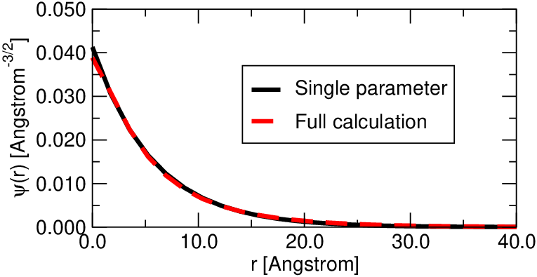
The full variational solution computed using 50 parameters is plotted in Fig. 15, where it is also compared to a single parameter variational solution. The single-parameter solution with gives a remarkably accurate approximation for the wave function, excepting the regime , where small deviations appear due to the central cell correction.
A.2 Calculation of on-site optical matrix elements
Once the variational wave function (43) is known (at hand), we can compute the optical matrix elements to valence band states. We have two obvious choices: The simplest way to estimate these matrix elements is to neglect the term as well as the central cell correction (which does not interact too much with the -channel), and to use free electron states
| (45) |
with the spherical Bessel functions and spherical functions. Alternatively, we can neglect only the central cell correction and use Coulomb scattering states,
| (46) |
where is related to the confluent hypergeometric function, , as
| (47) |
with , the constant , and the gamma function. Both scattering states are normalized to satisfy .
The matrix elements of can be computed analytically in both cases. For free valence electrons we obtain
| (48) |
while for Coulomb scattering states we have
The matrix elements obtained this way were presented in Fig. 6. The single parameter ground state wave function gives a very good approximation in both cases. The overall energy dependence of the transition matrix elements is qualitatively similar in Coulomb and the free scattering state approximations. However, the height of the peak is about a factor of two larger in the free electron approximation.
Appendix B Two site problem
In this Appendix we determine the energies of the molecular orbitals of an system and use them to calculate the parameters of an effective second quantized Hamiltonian. We consider two Mn ions, located at positions , and described by the Hamiltonian of Eq. (3). Similar to the Mn ion case, we first construct the lowest lying ’molecular states’ using variational wave functions of the form,
| (49) |
constructed from Hydrogen-like and -type wave functions centered at the Mn sites,
| (50) | |||
| (51) |
Here is the direction connecting the two sites, and denote the position of the valence hole relative to . We considered only states that do not have a mirror plane that contains , and therefore included only orbitals. Similar to Appendix A, we fix the parameters in Eq. (49), and consider only the as variational parameters.
As in case of the single Mn ion problem, the coefficients satisfy a set of linear equations,
| (52) |
with the overlap matrix elements and the Hamiltonian matrix elements defined as
The above integrals can be performed analytically using elliptic coordinates. Some details of the derivation as well as the analytical expressions are given as an on-line supplement.
We remark here that Eq. (52) not only provides an accurate estimate for the ground state energy, but it also accounts for the first few excited states. In Fig. 16 we show the first few lowest energy states obtained in this way as a function of Mn separation, . As demonstrated in the figure, the inclusion of -orbitals does not result in a major improvement for the first five states, though it introduces a level crossing between the first and the second excited states at a distance where the tight-binding approximation fails.

The hopping and the energy appearing in Eq. (5) and shown in Fig 4 can be extracted from this spectrum as:
where and represent the lowest lying (even) state of the molecule and that of the first (odd) excited state.
The electric field induces transitions between the previously-mentioned even and odd states, and thereby generates a coupling of the form, Eq. (11). To determine the parameters appearing in this equation, one simply needs to compute the momentum matrix elements that enter the coupling to the external electromagnetic field. Since we aligned the two ions along the direction the only non-vanishing component of the momentum matrix elements is . It is possible to express this matrix element analytically for our variational wave functions, though the final expressions are rather cumbersome. The final results have been plotted in Fig. 5.
References
- [1] H. Ohno and F. Matsukura Sol. Stat. Comm. 117 179 (2001).
- [2] G. Zarand, C. P. Moca, and B. Janko, Phys. Rev. Lett. 94, 247202 (2005); C. P. Moca, B. L. Sheu, N. Samarth, P. Schiffer, B. Janko, and G. Zarand, Phys. Rev. Lett. 102, 137203 (2009).
- [3] C. Timm, M. E. Raikh and F. von Oppen, Phys. Rev. Lett. 94, 036602 (2005).
- [4] V. Novak, K. Olejnik, J. Wunderlich, M. Cukr, K. Vyborny, A. W. Rushforth, K. W. Edmonds, R. P. Campion, B. L. Gallagher, Jairo Sinova, and T. Jungwirth, Phys. Rev. Lett. 101, 077201 (2008).
- [5] M. P. Lopez-Sancho and L. Brey, Phys. Rev. B 68, 113201 (2003).
- [6] T. Jungwirth, Q. Niu, and A. H. MacDonald, Phys. Rev. Lett. 88, 207208 (2002).
- [7] J. Okabayashi, A. Kimura, O. Rader, T. Mizokawa, A. Fujimori, T. Hayashi, and M. Tanaka, Phys. Rev. B 64, 125304 (2001).
- [8] D. Kitchen, A. Richardella, and A. Yazdani, J. Supercond. 18, 23 (2005); A. M. Yakunin, A. Y. Silov, P. M. Koenraad, W. Van Roy, J. De Boeck, and J. H. Wolter, Physica E 21, 947, (2004).
- [9] E. J. Singley, K. S. Burch, R. Kawakami, J. Stephens, D. D. Awschalom, and D. N. Basov, Phys. Rev. B 68, 165204 (2003).
- [10] E. J. Singley, R. Kawakami, D. D. Awschalom, and D. N. Basov, Phys. Rev. Lett. 89, 097203 (2002).
- [11] K. S. Burch, D. B. Shrekenhamer, E. J. Singley, J. Stephens, B. L. Sheu, R. K. Kawakami, P. Schiffer, N. Samarth, D. D. Awschalom, and D. N. Basov, Phys. Rev. Lett. 97, 087208 (2006).
- [12] K. S. Burch, E. J. Singley, J. Stephens, R. K. Kawakami, D. D. Awschalom, and D. N. Basov, Phys. Rev. B 71, 125340 (2005).
- [13] M. Linnarsson, E. Janzén, B. Monemar, M. Kleverman, and A. Thilderkvist, Phys. Rev. B 55, 6938 (1997).
- [14] T. Jungwirth, J. Sinova, A. H. MacDonald, B. L. Gallagher, V. Novák, K. W. Edmonds, A. W. Rushforth, R. P. Campion, C. T. Foxon, L. Eaves, E. Olejnk, J. Masek, S.-R. Eric Yang, J. Wunderlich, C. Gould, L. W. Molenkamp, T. Dietl, and H. Ohno, Phys. Rev. B 76, 125206 (2007).
- [15] W. Songprakob, R. Zallen, D. V. Tsu, and W. K. Liu J. Appl. Phys. 91 171, (2002).
- [16] S.-R. Eric Yang, J. Sinova, T. Jungwirth, Y. P. Shim, and A. H. MacDonald, Phys. Rev. B 67, 045205 (2003).
- [17] M. Turek, J. Siewert, and Jaroslav Fabian, Phys. Rev. B 78, 085211 (2008).
- [18] E. H. Hwang, A. J. Millis, and S. Das Sarma, Phys. Rev. B 65, 233206 (2002).
- [19] A.-T. Hoang, Physica B 403 1803 (2008).
- [20] G. Alvarez and E. Dagotto, Phys. Rev. B 68, 045202 (2003).
- [21] J. S. Blakemore, W. J. Brown, M. L. Stass, and D. A. Woodbury, J. Appl. Phys. 44, 3352 (1973).
- [22] G. A. Fiete, G. Zarand, K. Damle, and C. P. Moca, Phys. Rev. B 72, 045212 (2005)
- [23] A. K. Bhattacharjee and C. B. á la Guillaume, Solid State Comm. 113, 17 (2000); S.-R. Yang and A. H. MacDonald, Phys. Rev. B 67, 155202 (2003).
- [24] T. Jungwirth, J. Sinova, J. Maek, J. Kucera, and A. H. MacDonald, Rev. Mod. Phys. 78, 809 (2006).
- [25] D. A. Woodburry and J. S. Blakemore, Phys. Rev. B 8, 3803 (1973).
- [26] R. Moriya and H. Munekata, J. Appl. Phys. 93, 4603 (2003).
- [27] M. Poggio, R. C. Myers, N. P. Stern, A. C. Gossard, and D. D. Awschalom, Phys. Rev. B 72, 235313 (2005).
- [28] K. M. Yu, W. Walukiewicz, T. Wojtowicz, I. Kuryliszyn, X. Liu, Y. Sasaki, and J. K. Furdyna, Phys. Rev. B 65, 201303 (2002).
- [29] A. Oiwa, S. Katsumoto, A. Endo, M. Hirasawa, Y. Iye, H. Ohno, F. Matsukura, A. Shen, Y. Sugawara, Solid State Commun. 103, 209 (1997).
- [30] F. Matsukura, H. Ohno, A. Shen, and Y. Sugawara, Phys. Rev. B 57, R2037 (1998).
- [31] A. Van Esch, L. Van Bockstal, J. De Boeck, G. Verbanck, A. S. van Steenbergen, P. J. Wellmann, B. Grietens, R. Bogaerts, F. Herlach and G. Borghs, Phys. Rev. B 56, 13103 (1997)
- [32] H. Shimizu, T. Hayashi, T. Nishinaga, M. Tanaka, Appl. Phys. Lett. 74, 398 (1999).
- [33] M. Berciu and R. N. Bhatt, Phys. Rev. Lett. 87, 107203 (2001).
- [34] J.König , T. Jungwirth and A. H. MacDonald, Phys. Rev. B 64, 184423 (2001).
- [35] H. Ohno, N. Akiba, F. Matsukura, A. Shen, K. Ohtani, and Y. Ohno, Appl. Phys. Lett. 83, 6548 (1998)
- [36] A. K. Bhattacharjee and C. B. A á la Guillaume, Solid State Comm. 113, 17 (2000).
- [37] B. L. Altshuler and A. G. Aronov, Electron-electron Interactions in Disordered systems, Edited by A.L. Efros and M. Pollak, Elseview Science Publisher, 1985.
- [38] E. Abrahams, P. W. Anderson, D.C. Licciardello, and T. V. Ramakrishnan Phys. Rev. Lett. 42, 673, (1979).
- [39] B. Shapiro, and E. Abrahams, Phys. Rev. B 24, 4889 (1981).
- [40] P. Lambrianides, and H. B. Shore, Phys. Rev. B 50, 7268 (1994).
- [41] H. Shima, and T. Nakayama, Phys. Rev. B 60, 14066 (1999).
- [42] A. Weiße, G. Schubert, and H. Fehske, Physica B 359-361, 786 (2005).
- [43] J. Schliemann and A.H. MacDonald, Phys. Rev. Lett. 88, 137201 (2002).
- [44] G. Zarand and B. Janko Phys. Rev. Lett. 89, 047201 (2002)
- [45] A. Kassaian and M. Berciu, Phys. Rev. B 71, 125203 (2005).
- [46] M. Berciu and R. N. Bhatt, Phys. Rev. B 69, 045202 (2004).