Calibration and Interpixel Capacitance of a H2RG(2Kx2K) Near-IR Detector
Abstract
A temporal analysis of the noise is performed, and non linearities are taken into account. We then extend the correlation method to groups of several pixels to derive the interpixel capacitance of a detector, found to be x = -0.0263 0.0020 (stat)0.0040 (syst.) All measurements are consistent to a sub-percent accuracy.
1 The Apparatus
The measurements described in this paper were carried out in a dedicated setup built to evaluate Hawaii detectors H2RG from Teledyne (ex Rockwell). The detector was on loan from LBNL in view of the evaluation of its performance when used in a spectrograph for the JDEM project [1]. The cryostat can be operated in a range of temperature extending from 100K to 160K with fluctuations smaller than 0.1 K, and its equilibrium temperature in the absence of heating is about 110K. It was designed so as to ensure a variation rate of temperature smaller than 0.5 K/minute whatever the liquid Nitrogen flow. A mirror located in the cryostat ensures a uniformity of illumination better than 1% over the full detector in the tests described in this paper.
The readout cards were adapted from the acquisition system of the OPERA neutrino experiment. Their schematic layout is shown in Figure 1, and their configuration on the cryostat in Figure 2. This acquisition system was actually used in the tests performed on the SNAP Spectrograph demonstrator in the Near infrared range [2, 3].
2 The calibration scheme
We adopt the standard method of calibration as in [4, 5] taking advantage of the stochastic Poisson fluctuations from frame to frame under illumination by a Light Emitting Diode. The overall variance will be the sum of the contributions from readout noise, common mode noise, and stochastic noise, the latter being easy to extract since it is the only one to depend on illumination. The H2RG detectors have been extensively tested in the SNAP context as reported in [6, 10]. These authors also investigated the spatial correlations of the signal noise. The method proposed here is a variant where the emphasis is on a redundant determination of the interpixel capacitance using groups of pixels, and a temporal analysis of the LED signal is performed, as would occur in an actual flux measurement. Non linearities are taken into account.
The ADC responds to a voltage change between two frames according to
where the calibration coefficient is the product of the
emitter-follower factor ( 0.85) and of the ADC conversion factor
(70 , and is the pixel voltage.
For each LED setting, 7 to 10 consecutive measurements were performed. The first two were ignored as the detector is not in a stationary regime, and the last five were averaged to obtain our results. The spread between consecutive exposures with the same LED intensity was used to estimate the measurement errors: their origin is NOT statistical, NOR due to a slow variation of the LED intensity.
In a single pixel detector, the voltage change is linearly related (in the appropriate conditions) to the number of electron stored as where is the number of electrons stored in the pixel, the electron charge, and the capacitance of a single pixel, quoted by Teledyne as 40ff. The conversion factor is then expected to be
The stochastic fluctuation of the charge on the pixel is , and the variance (time average) of the ADC readouts between two frames arising from Poisson fluctuations is Where is the accumulated number of electrons between the two frames considered (to be distinguished from the fluctuation of this number).
We can substitute which yields
| (1) |
The conversion factor is the inverse of the slope in the relation between the variance of the stochastic contribution to the noise (in ADC units) in a given time, and the flux accumulated during the same time (also in ADC units). The capacitance of the pixel can be obtained once has been measured.
In a multipixel detector, we adopt a description close to the one proposed by [12], but more general. The charge in pixel is now also dependent on the voltage in pixel , and the relation is given by the electrostatic influence matrix. (summation is implied). The ADC response in pixel , will be given by:
where is the change in the number of electrons in pixel . The stochastic noise of pixel can again be derived from the Poisson fluctuations in the pixels
If diffusion is negligible, there is no correlation in the numbers for different pixels,and the time average of the product is (where is the Kronecker matrix, and the nb of electrons collected in pixel between consecutive frames. Using we then find
So that
| (2) |
This general expression will now be simplified by the use of convenient approximations of the matrices and . If we consider only the coupling of adjacent pixels, with ( is negative) in a homogeneous detector, as in [4], the influence matrix for a group of 5 pixels centered on pixel as shown in Figure 3b) is , where the matrix is of the form
This matrix can be inverted exactly, but as the electrostatic coupling ratio will be found to be small, the inverse matrix can be obtained by substituting to when the second order terms are neglected.
We have now obtained for the single pixel noise of a homogeneous detector
evaluating the variance from both sides of this formula, we find:
As the illumination is uniform, all fluxes are equal and the mean flux in pixel is
| (3) |
Under a uniform illumination, the conversion factor (e/ADCU) was however found to be
so that
| (4) |
As is negative, the conversion factor will now be smaller than the inverse of the slope, and smaller than expected for a ’single pixel’. The edge effect from adjacent pixels is expected to decrease for larger groups of pixels, and the relation between slope and conversion factor should be closer to the single pixel case.
3 Noise fluctuations for groups of pixels
The previous formulae allow us to measure the ratio by comparing the relation
between noise and flux for groups of pixels, as this changes the weight of the contribution
of the neighbouring pixels.
2 pixel groups (as shown in Figure 3a)
The capacitance matrix to be considered follows from Fig. 3 a):
For a typical value of , the diagonal elements of the inverse
matrix vary from 1.0004 to 1.0016, while the off-diagonal elements of adjacent
pixels differ from 0.02 by less than , the other coefficients
are smaller than . Neglecting all small offsets, we find:
and substituting for the expression of in terms of the observed ADC shift
in 1 pixel between frames
| (5) |
5 pixel groups (Figure 3b)
We find in the same way:
So that
and using as before the relation between and , the ADC shift:
| (6) |
9 pixel groups (Figure 3c)
and for 9 pixels forming a square (see Figure 3):
| (7) |
4 The measurement method
The cryostat temperature was set at 110K, the equilibrium value in the absence of any heating, during these tests. In contrast with previous publications, which used the spatial correlations under different illumination conditions ([7]), we have used the time variation of the signal to evaluate the noise and the correlation, as a training for the flux measurements anticipated in the near future. The frames are grouped into ’bursts’, the number of frames in each burst decreasing from 60 (LED current of 10 A), to 15 (LED current of 100 A). The variance of the differences of readouts for consecutive frames is then evaluated for each pixel, and each burst, and the measurement is repeated ’up the ramp’ until saturation is reached. The results are then averaged over all pixels for each burst. At any LED setting at least 10 exposures are taken to allow control of the error estimates.
4.1 Non-linearities
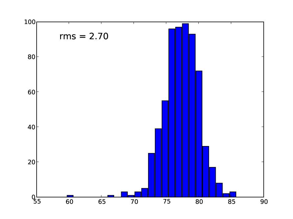
The distribution of the flux in ADC units averaged over all bursts for all pixels at a typical setting with a LED current of 40 A is shown in Figure 4 a). It is seen that in the absence of flatfielding corrections, its spread is 3.5%. This good homogeneity of the detector in the analysis window allows averageing of the measured properties over all pixels (the flux and variance of each pixel is still evaluated independently). A linear variation of and of the single pixel noise along the ramp is then observed in Figure 4 b). As the flux measurement is perfectly reproduced from one exposure to the next, the flux variation is an indication of the non-linear response of the system. The most likely source of this behaviour is the output FET, and the observations suggest a decrease of the transconductance as the grid voltage decreases with an increasing number of trapped electrons in the pixel well. The slopes of the variance and of the flux (normalised to their value at an output ADC value of 19000 ADCU) are respectively and , and they correspond to similar (and opposite) relative variations, as expected if the equivalent thermal resistor is the inverse of the transconductance. The effective conversion factor given by the ratio variance/flux cannot be obtained without further corrections. All the following analyses have been performed with 2 different extrapolations, namely to the middle (32500) and to the lower values (10000) of the ADC dynamical range. To crosscheck the validity of the corrections, different LED illuminations will be compared. The conversion factors found are expected to differ by 5% as a consequence of the non linear response, but the interpixel capacitance obtained should be the same up to systematic errors.
| Pixel | var(ADCU) |
|---|---|
| group | |
| 1 | 121.02 0.77 |
| 2-H | 249.17 1.50 |
| 2-V | 261.24 1.79 |
4.2 The 2 pixel pairs
It is intructive to consider separately horizontal (readout direction) and vertical pairs of pixels. Horizontal pairs are read consecutively, while vertical pairs are separated by the time interval needed to complete the readout of the intermediate pixels. The variance quoted in Table 1 is obtained in the absence of any illumination by summing 2 pixels, measuring the difference between consecutive frames, estimating its variance for each burst (of typically 60 frames), averaging over all bursts, and then over all pairs. The result for the mean variance is given.
It is seen that intrinsic voltage changes in the chip during the readout impact the variance a level of about 4%. Analyse is in progress to shown soon results including a temporal common mode correction by subtracting a reference channel.
4.3 The 5 and 9 pixel configurations
The measured values of the variance and the flux for each pixel grouping is shown in figure 5 for 12 illumination conditions. The expected linear relation (after correcting for the non-linear response!) is observed in Figure 5 for the data and the slopes found from the extrapolation to lower flux values are given in Table 2.
The ratio of the interpixel capacitance to the pixel capacitance is found from the comparison of the slopes for 1,2,5,and 9 pixels: To modify the impact of the fluctuations from adjacent pixels, we now evaluate their contribution to the variance of larger groups of pixels. The interpixel capacitance can then be derived for each pixel grouping from equations (5),(6),(7).
4.4 Conversion factor and effective Interpixel capacitance
| pixel | Slope |
|---|---|
| group | |
| 1 | 0.4021 0.0026 |
| 2 | 0.8458 0.0049 |
| 5 | 2.2139 0.0218 |
| 9 | 4.2095 0.0550 |
The values of the interpixel capacitance found in all cases are given in Table 3 with the linearity correction extrapolated to the lower ADC range (10000). They are compatible, with small residual systematic shifts, and we shall perform a weighted average.
| Group | ratio | x |
|---|---|---|
| s2/s1 | 2.1028 0.0183 | -0.02455 0.00416 |
| s5/s1 | 5.5063 0.0651 | -0.02947 0.00352 |
| s9/s1 | 10.4696 0.1529 | -0.02916 0.0029 |
The value . The same averages performed at ADCU = 30000 leads to For our final result, we take the average of the two estimates and attribute a systematic error of 0.0040 to account for the small difference in the non-linearity corrections (mid range and low range).
The (single pixel) conversion factor in the lower ADC range can now be obtained as
and it is 10% larger at full well. The conversion factors found in the 2 extrapolation methods differ by 5%, as expected from the nonlinear behaviour seen in figure 4b): they are evaluated at different values of the ADC range. The result is very close indeed to the value of 2.15 derived from an assumed pixel capacitance of 40ff in section 2.
4.5 Diffusion and actual Interpixel capacitance
The effective value of the interpixel capacitance found would NOT be the true value if ’fast’ diffusion would occur as suggested by [6]: while the interpixel capacitance increases the fluctuations, diffusion from one pixel to the adjacent ones would reduce them. A detailed computation shows that the contribution to from diffusion is equal to the fraction of electrons migrating to the adjacent pixel for 2 and 5 pixel groups, but is only for the 9 pixel group. Given the consistency of the previous results between 9 and 5 pixel groups, we obtain (3 limit).
5 Conclusions
A general correlation method has been proposed, which allows strong cross-checks for internal consistency of the observations between different pixel groups. We have shown that the non-linearities which are seen are consistent with the effect of a transconductance variation in the output FET of the detector,and that they can be corrected to a sub-percent accuracy. The remaining systematic errors are in the range. It has also been shown that the use of the reference channel have to studied in that frame of work. The imapct of that studies will be shown in a forthcoming paper. The calibration of the readout set-up will be studied in order to describe the noise performance achieved under different conditions.
6 Acknowledgements
We thank all the institutions who have supported us during this work: Université Claude Bernard Lyon 1, The IN2P3/CNRS institute, and the engineers and technicians at IPNL and CPPM who have contributed to the apparatus JC Ianigro, A. Castera, and in particular C. Girerd who has designed the readout electronics. We are indebted to C. Bebek (LBNL) for lending us the H2RG detector, and to G. Tarle, M. Schubnell, and R. Smith for many questions and suggestions.
References
- [1] M.-H. Aumeunier et al. Proc. SPIE 6265,626534 (2006) An integral Field Spectrograph Demonstrator based on a slicer
- [2] C. Cerna et al. Proc. SPIE Vol. 7010,7010A(2008);DOI:10.1117/12.789583 Setup and performance of the SNAP spectrograph Demonstrator
- [3] M-H. Aumeunier et al. Proc. SPIE Vol. 7010, 70103N(2008);DOI:10.1117/12.789587 First results for the spectro-photometric calibration of the SNAP spectrograph Demonstrator in the visible range
- [4] G. Finger et al. Performance Evaluation and calibration issues of large Format Infrared Hybrid active pixel sensors (NIM A Vol. 565,1 (Sept 2006)2008
- [5] G. Finger et al. Performance Evaluation,readout modes, and calibration techniques of HgCdTe Hawaii-2RG mosaic arrays SPIE2008,Marseille
- [6] N. Barron, M. Borysow, K. Beyerlein, M. Brown, C. Weaverdyck, W. Lorenzon, M. Schubnell, G. Tarlé and A. Tomasch Proceedings of the Astronomical Society of the Pacific 119, 466-475,2007 Sub-Pixel Response Measurement of Near-Infrared Sensors
- [7] M. Brown,M. Schubnell, G. Tarlé PASP 118:1443-1447,2006 Correlated Noise and Gain in Unfilled and Epoxy-Underfilled Hybridized HgCdTe Detectors Sub-Pixel Response Measurement of Near-Infrared Sensors
- [8] M.G. Brown, et al., Proc. SPIE Vol. 6265, 626535 (2006). Development of NIR Detectors and Science Driven Requirements for SNAP
- [9] M. Schubnell, et al. Proc. SPIE Vol. 6276, 62760Q (2006).
- [10] R. Smith, et al., Proc. SPIE Vol. 6276, 62760R (2006) Noise and Zero Point Drift in 1.7 m Cutoff Detectors for SNAP Near Infrared Detectors for SNAP
- [11] S. Seshadri, et al. Proc. SPIE Vol. 6276, 62760S (2006). Characterization of NIR InGaAs Imager Arrays for the JDEM SNAP Mission Concept
- [12] P. R. McCullough et al. PASP 120:759-776,July2008 Quantum Efficiency and Quantum yield of an HgCdTe Infrared Sensor Array