Disordered Electrical Potential Observed on the Surface of SiO2 by Electric Field Microscopy
Abstract
The electrical potential on the surface of nm thick SiO2 grown on single crystalline Si substrates has been characterized at ambient conditions using electric field microscopy. Our results show an inhomogeneous potential distribution with fluctuations up to V within regions of m. The potential fluctuations observed at the surface of these usual dielectric holders of graphene sheets should induce strong variations in the graphene charge densities and provide a simple explanation for some of the anomalous behaviors of the transport properties of graphene.
pacs
73.20.At,73.30.+y,73.61.JcNowadays, the study of graphene, i.e. a monolayer of graphite, represents an important research field in physics and material science. Although studies of monolayers of graphite grown on different transitional metal carbides have been already published nearly 20 years ago [1, 2], the simple preparation of these monolayers by exfoliation [3] as well as grown on SiC substrates [4] and their transport properties with the field effect dependence increased substantially the attention of the solid state community. One of the highlighted effects is the electric field-induced metal-insulator-semiconductor transition that populates the bands of graphene with holes or electrons, bands that have been claimed to be Dirac like, i.e. following a linear dispersion relation . Also, the observation of quantum Hall effects and the quantization of the conductance has been claimed [5]. There are many interesting published results that may suggest that one can achieve a new electronic basis with this material if, among other details, one would find a way to produce homogeneous, uniform layers or with a selective kind of defects enabling then their integration in devices [6].
There are, however, some experimental facts indicating that the transport behavior in graphene is far from being ideal. For example, the carrier mobility in samples on dielectric substrates including SiO2 is of the order of 1 m2/Vs, a value that remains rather independent of the dielectric substrate, temperature and density of carriers, see e.g. Ref. 7 and Refs. therein. On the other hand if the experiments are done with suspended graphene samples, i.e. without touching the substrate, the mobility drastically increased [8, 9]. The experimental data suggest that one of the main problems of graphene on dielectric substrates could come from the substrate non-uniform electrical potential.
It is generally known that oxides do not exhibit an uniform potential distribution because a distribution of charges in their near-surface region exists, letting a metastable charge-potential distribution on it. In this case the deposited graphene will be strongly affected by the same variations of potential the dielectric substrate has. It is interesting to note the results of an experimental study using a scanning single electron transistor that observed puddles of electrons and holes at the graphene surface [10]. The obtained images reveal a rather disordered domain-like array of fluctuating potential, which might be due to the substrate influence and not intrinsic of graphene. Further evidence for the potential influence comes out from the fact that in transport experiments done in graphene samples one needs to apply a magnetic field to increase the sample conductivity arguing that otherwise the carriers are localized [11]. In this work we argue that several of these observations and effects are due to the influence of the dielectric substrate potential at its near-surface region. Because of the previous arguments we would like to use the electric field microscopy (EFM) to analyze the surface of the SiO2 and try to see if we have potential fluctuations and measure their magnitude. This will tell us what is the initial state of the potential graphene sees before shifting the electron and hole bands via a bias voltage.
Consider an EFM arrangement shown schematically in Fig. 1(a) where a potential is applied between the metal tip and the surface of the oxide sample. The potential difference between tip and surface will be neither zero nor constant at the surface of SiO2. The applied electric field will penetrate in the oxide a certain penetration depth that depends on the total screening characteristics of the material. Due to the vanishingly low carrier density of SiO2 it is expected that the electric field penetration depth ( is the effective mass) would be nm for carrier density cm-3. Note that there is a large electrical resistance between the point of the surface where the tip is and the contact to mass. Therefore the bias voltage applied is between the tip and the thick oxide layer and the potential drop between the sample tip-position and the contact on the surface to mass (distance in Fig. 1(a)). Notice however that the last potential drop will be constant in all the measurements because the scan we perform is of the order of m2 and the distance from the tip-position to the contact is mm.

The samples we used are usual p-type, polished Si substrates (100) (Crystec, Germany) with resistivity cm) and a nm thick amorphous SiO2 at the surface grown by thermal annealing. Some of the substrates were covered by a layer of insulating optical resin (Pietlow Brandt GmbH, Germany) that was partially removed with ethanol in some of the samples to investigate the influence of resin rest on the EFM signal. Other Si substrates without resin coverage were also measured. The measurements at ambient conditions were done with two EFM microscopes: an AFM from NTI Solver and a Dimension 3000 with Extender Electronics Module from Veeco. The results presented in this work were obtained using the EFM mode in both. Two different conductive cantilevers were used: Olympus OMCL-AC240T M-B2, Pt-coated and W2C coated tips with resonance frequencies around 150.1 kHz and 76.3 kHz. The measurements were performed in the tapping/liftTM two-pass mode, measuring first the topography and then the frequency shift of the cantilever due to the electrostatic force between the tip and surface. At the first tapping mode no voltage is applied to the tip. If we apply a constant voltage to the tip and scan the sample surface at a constant distance from the sample following the track obtained in the first pass, the measured signal indicates the potential fluctuations on the sample. In the experiment the frequency shift from resonance depends linearly on the force gradient given by
| (1) |
where is the voltage difference applied between the tip of the cantilever and the surface and is the electrical potential that interacts with the cantilever tip. It depends on the potential due to charge distribution on the sample near-surface region and the difference of work functions between the tip and surface. Within a simple picture one tends to write , however both terms of the r.h.s are interrelated since differences in charge at the surface would imply also a change in work function. Because the exact value of is not known due to the further potential drop within the sample, our results are plotted as a function of the bias voltage that we applied. In the experiments we obtain an effective force gradient signal in nA units, which is proportional to force gradient given in Eq. (1). As explained in Ref. 12, taking the proportionality between these signals (or their square root) and , a calibration is done that is used to transform the measured signals in nA units to voltage potential changes. In this way any further calibration in terms of the real force gradient is unnecessary.

Figure 2 shows the measured signals vs. at different positions of the SiO2 surface and at different distances . The result of having the minima of the signal out of zero, see Fig. 2(a), is not always observed because of the potential fluctuations. There are other points where the potential falls around zero as we show in Fig. 2(b). In this case the effective force gradient signal between -5V and 5V and for tip height between 50 nm and 1000 nm is shown. We observe that all the curves are centered at V and the curves are practically symmetric with maximum values for 50 nm and minimum for 1000 nm. The amplitude of vibration of the cantilever is nm and then for nm the signal depends partially on this vibration. For nm the signal is independent of the usual vibration amplitudes but with a relatively large noise to signal ratio. The best performances are obtained for 100 nm nm. The results below were obtained for nm. The results presented in Fig. 2 validate the quadratic dependence given by Eq. (1). The EFM results presented below are therefore obtained at constant distance and bias voltage and all the changes in the effective force gradient we measure are due to changes in the function .
We have to verify now that the capacitor model describes the experiments. Consider the prefactor of Eq. (1). If we have a capacitor defined between the tip and surface, then
| (2) |
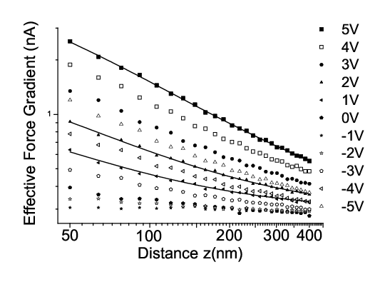
where is a geometrical factor characteristic of the tip-surface arrangement. In the denominator we have the variation with distance tip-surface and is an effective penetration depth of the electric field in the SiO2. Note that for a metal is practically zero but this is not so for an insulator as shown by the results presented in Fig. 3 where the EFM signal vs. distance at constant is plotted. If our system has a deviation from planar electrodes the exponent in Eq. (2) should be smaller than 3. This is what we observe from fitting the results in Fig. 3 obtaining and nm for a region with higher carrier concentration (bright spot) and nm for a region with lower carrier concentration (dark spot), as expected. The dark regions have less charge and the field should penetrate more.
We now proceed to take topographical data with AFM and then on the same scan line EFM data to see the potential variations with respect to the AFM using the calibration mentioned above. Figure 4 shows the AFM (left) and EFM (right) pictures taken on a different substrate as those shown in Fig. 1(c) and (d) (we have taken more than 50 scans of this kind in 6 substrates and all look the same). The white spots correspond to the resin rest that we left to demonstrate that this rest is not the cause of the relatively broad variation of the surface potential and it does not prevent of measuring the topography and potential fluctuations. Similar results are obtained from a sample without any resin rest, see Fig. 1(d). The lower pictures in Fig. 4 show the scans through the lines (1) to (3) shown in the upper pictures. We observe large fluctuations in white and black regions through the entire sample. It is clear from the EFM figures that the oxide surface shows relatively large potential fluctuations within microns between 0.1 V and 0.3 V for that sample. Following a similar treatment as in Ref. 13 this potential can be produced by a charge density equivalent to electrons per m3. Note that upon region one can also observe potential fluctuations within a distance of m. Note that topographic changes in AFM do not influence the EFM signal. All the curves obtained between 100 nm to 600 nm show the same potential variations because these do not change with the applied voltage indicating that the topography measurement in the tapping mode scan is reliable. We checked that all measured EFM signals provide the complementary contrast by reversing the voltage polarity applied at the tip indicating that those signals are due to potential variations and not due to capacitance artifacts, as explained in detail in Ref. 12.

The overall EFM results (Figs. 1 and 4) mean that a graphene layer located on these surfaces will feel directly the potential fluctuations producing regions with higher density of carriers (electrons as well as holes) at the minima (or maxima) and extended regions with a smaller carriers’ density. In this case the carriers can be partially localized, see sketch in Fig. 1(b), and there will be no conductance unless one applies a large enough magnetic field or bias voltage as observed experimentally [11]. The influence of these potential fluctuations on dielectric substrates may also explain the observation of the quantum Hall effect (QHE), which is apparently not observed for graphene layers with smaller fluctuations or “better” quality. We note also that whereas clear signs of the QHE are observed in macroscopic HOPG samples [14, 15] it appears to be absent in mesoscopic multigraphene samples of good quality [16]. Another aspect is that the so-called Dirac point - claimed to have been reached by some experimentalists in their experiments [5] - has not been actually reached. The carrier density at the Dirac point is several orders of magnitude smaller that the apparent reached minimum of cm-2. Note also that a graphene sample on such a disordered potential distribution indicates that the use of a bias voltage on the transport properties does not assure at all a Dirac point crossing through the sample. We note that although a linear dispersion relation for carriers is observed in different spectroscopic experiments, the existence of a Dirac point at sufficiently low energies has not yet experimentally proved for graphene/graphite. Another point is that the number of carriers is difficult to determine because in real graphene samples and due to the influence of the substrate and/or attached borders for suspended samples there will be regions with many and regions without carriers at low enough temperatures, see Fig. 1(b). We would like to remark that our EFM results have m resolution. At smaller distances there could be additional charge distributions that can also have strong influence on the carrier mobility of the graphene carriers. The here found inhomogeneous potential distribution on a dielectric substrate provides a simple way to understand the experimentally observed constancy of the carrier mobility on dielectric substrates [7].
In conclusion, EFM measurements on SiO2 surfaces reveal a disordered potential structure of hills and valleys similar to those observed using a single electron transistor on graphene [10], which are due to intrinsic fluctuations of the dielectric substrate. The potential variations can reach hundreds of mV and therefore the carriers of graphene attached on a dielectric substrate will have difficulties to move through the sample affecting their mobility. These results may explain several unclear behaviors reported in literature on this topic.
We gratefully acknowledge the support of the DFG under DFG ES 86/16-1, the DAAD under Grant No. D/07/13369 (“Acciones Integradas Hispano-Alemanas”) and the Spanisch DGICyT. One of us (N.G.) is supported by the Leibniz Professor fellowship of the University of Leipzig.
References
- [1] T. Aizawa, R. Souda, S. Otani, Y. Ishzawa, and C. Oshima, Phys. Rev. Lett. 64, 768 (1990).
- [2] H. Itoh, T. Ichinose, C. Oshima, and T. Ichinokawa, Surface Science Letters 254, L437 (1991).
- [3] K. S. Novoselov, A. K. Geim, S. V. Morozov, S. V. Dubonos, Y. Zhang, and D. Jiang, Science 306, 666 (2004).
- [4] C. Berger, Z. Song, X. Li, X. Wu, N. Brown, C. Naud, D. Mayou, T. Li, J. Hass, A. N. Marchenkov, et al., J. Phys. Chem. B 108, 19912 (2004).
- [5] A. K. Geim and S. Novoselov, Nature Materials 6, 183 (2007), and Refs. therein.
- [6] M. Orlita, C. Faugeras, P. Plochicka, P. Neugebauer, G. Martinez, D. K. Maude, A.-L. Barra, M. Sprinkle, C. Berger, W. A. de Herr, et al., Phys. Rev. Lett. 101, 267601 (2008).
- [7] L. A. Ponomarenko, R. Yang, T. M. Mohiuddin, M. I. Katsnelson, K. S. Novoselov, S. V. Morozov, A. A. Zhukov, F. Schedin, E. W. Hill, and A. K. Geim, Phys. Rev. Lett. 102, 206603 (2009).
- [8] K. I. Bolotin, K. J. Sikes, Z. Jiang, M. Klima, G. Fudenberg, J. Hone, P. Kim, and H. L. Stormer, Solid State Commun. 146, 351 (2008).
- [9] X. Du, I. Skachko, A. Barker, and E. Y. Andrei, Nature Nanotech. 3, 491 (2008).
- [10] J. Martin, N. Akerman, G. Ulbricht, T. Lohmann, J. H. Smet, K. von Klitzing, and A. Yacoby, Nature Phys. 4, 144 (2008).
- [11] S. V. Morozov, K. S. Novoselov, M. I. Katsnelson, F. Schedin, D. C. Elias, J. A. Jaszczak, and A. K. Geim1, Phys. Rev. Lett. 100, 016602 (2008).
- [12] Y. Lu, M. Muñoz, C. S. Steplecaru, C. Hao, M. Bai, N. García, K. Schindler, and P. Esquinazi, Phys. Rev. Lett. 97, 076805 (2006), see also the comment by S. Sadewasser and Th. Glatzel, Phys. Rev. lett. 98, 269701 (2007) and the reply by Lu et al., idem 98, 269702 (2007); R. Proksch, Appl. Phys. Lett. 89, 113121 (2006).
- [13] K. Schindler, N. García, P. Esquinazi, and H. Ohldag, Phys. Rev. B 78, 045433 (2008).
- [14] Y. Kopelevich, J. H. S. Torres, R. R. da Silva, F. Mrowka, H. Kempa, and P. Esquinazi, Phys. Rev. Lett. 90, 156402 (2003).
- [15] H. Kempa, P. Esquinazi, and Y. Kopelevich, Solid State Communication 138, 118 (2006).
- [16] J. Barzola-Quiquia and P. Esquinazi, unpublished.