Non-Equilibrium and Quantum Coherent Phenomena in the Electromechanics of Suspended Nanowires
Abstract
Strong coupling between electronic and mechanical degrees of freedom is a basic requirement for the operation of any nanoelectromechanical device. In this Review we consider such devices and in particular investigate the properties of small tunnel-junction nanostructures that contain a movable element in the form of a suspended nanowire. In these systems, electrical current and charge can be concentrated to small spatial volumes resulting in strong coupling between the mechanics and the charge transport. As a result, a variety of mesoscopic phenomena appear, which can be used for the transduction of electrical currents into mechanical operation. Here we will in particular consider nanoelectromechanical dynamics far from equilibrium and the effect of quantum coherence in both the electronic and mechanical degrees of freedom in the context of both normal and superconducting nanostructures.
Keywords:
Nanoelectromechanical systems, electromechanical shuttling, NEM coupling, quantum coherence, non-equilibrium dynamics, superconducting weak linkspacs
73.23.-b, 73.63.Nm, 74.50.+r, 85.85.+jI Introduction
One of the main goals of contemporary nanophysics is to attain the means for controlled operation of mechanical devices on the nanometer length scale. The required coupling between electronic and mechanical degrees of freedom can be dramatically enlarged in conducting nanoelectromechanical systems (NEMS) where electrical currents and accumulated charge can be concentrated to small spatial volumes. Of particular interest in this Review are small tunnel structures that incorporate a movable element in the form of a suspended nanowire. This is because here, as we shall demonstrate below, one is able to harvest a host of mesoscopic phenomena for the purpose of transduction of electrical currents into nanomechanical operations.
One example of a nanoelectromechanical (NEM) device is the nanoelectromechanical single-electron tunneling (NEM-SET) transistor. Such a device may be built by self-assembly, employing mechanically soft organic molecules anchored at metal electrodes while attached to a small conducting ”Coulomb dot” or ”single-electron box” [1, 2]. In this way mechanical displacements of the dot with respect to the conducting leads are possible (see also Ref. [3]). Other approaches to building NEM-SET devices involve the use of a flexible nanopillar placed between a source and drain electrode [4] and placing a metal ”dot” on the tip of an externally driven cantilever [5]. Generally, in NEM-SET devices the transport of electrons is due to a combination of single-electron tunneling events (between either the source or the drain lead and the dot) and the mechanical transportation of charge through to the motion of the dot.
Mechanical vibrations can be coupled to the electron transport both via uncompensated charge (electrostatic coupling) and currents (magnetomotive coupling). An electrostatic coupling can be realized in devices where a nanomechanical resonator is used as a movable gate electrode [6, 7, 8]. In such nanoelectromechanical devices, where the movable part is effectively “zero-dimensional”, one has found that the electromechanical coupling can — under certain conditions — have much more dramatic results than simply vibron assisted tunneling, which follows from a straightforward application of perturbation theory. In particular, it has been shown that an electrostatic coupling of mechanical and electronic degrees of freedom can induce an electromechanical instability, resulting in self-sustained temporal oscillations in both the mechanical and electronic characteristics of the system. This instability is behind the new “shuttle” mechanism for mechanically promoted single-electron mesoscopic charge transport that was proposed in Ref. [9]. A number of the consequences of mechanically assisted “shuttle” transport have been investigated for normal, superconducting and magnetic NEM-SET devices (see, e.g., the reviews Ref. [10] and [11]).
Other frequently studied nanoelectromechanical systems are “one-dimensional” in the sense that they incorporate a suspended nanowire as a (possibly) vibrating current carrying element. In this case there are many more relevant mechanical degrees of freedom than in the rigid ”zero-dimensional” quantum-dot-type NEM devices. In the latter type of device it is sufficient to take the center-of-mass-motion of the movable element into account, while in the former also flexural and other types of wire vibrations, as well as intrinsic phonon modes, can couple to the electrons [12, 13, 14]. The effect of the various vibration modes on electron transport can be investigated either through the driven resonator method, where a down-mixing technique is used for detection [15, 16], or through scanning tunneling spectroscopy methods, detecting phonon-assisted channels for the inelastic tunneling of electrons [17, 18, 19].
A number of novel nanoelectromechanical phenomena become possible as a result of the elongation of the movable NEM-SET element. The present authors have, e.g., recently been involved in studies of the interplay in such devices between quantum coherence in both electronic and vibrational degrees of freedom. Other investigations have been related to non-equilibrium transport issues resulting from electromechanical instabilities that drive the system far away from equilibrium. This work will be reviewed in the present paper, where the following topics will be discussed.
- 1.
Multi-mode shuttle structures. The nanoelectromechanics of nanowire-based (“one-dimensional”) NEM-SET devices have to deal with the multimode flexural vibrations of the suspended wire, and their effect on charge transport. The relevant theoretical framework will be reviewed, and in particular we will show how a strong nonlinear coupling between different modes leads to a “self organization” effect in multimode shuttle structures.
- 2.
Interplay between quantum coherent mechanical vibrations and coherent electron transport. Quantum coherence is expected to play a significant role in the nanomechanics of sufficiently long suspended carbon nanowires, since the amplitude of their zero-point oscillations is comparatively large. The entanglement between quantum coherent electrons and quantum coherent mechanical vibrations, induced by an external magnetic field, will be shown to qualitatively modify the NEM-assisted electron transport in this case. This phenomenon suggests that measuring the magnetoresistance may be a way of testing quantum coherence in mechanical nanovibrations.
- 3.
Nanoelectromechanics of a superconducting weak nanowire-link. A current passing through a suspended wire of nanometer-sized cross-section in the presence of a transverse magnetic field, gives rise to a strong nanoelectromechanical coupling via both the Lorentz force and the electromotive force. We show that this coupling qualitatively changes the electrodynamics of a suspended nanowire serving as a superconducting weak link. The possibility to resonantly pump energy into nanowire vibrations by means of an AC Josephson current is explored.
The paper is organized as follows. In Section II we introduce the reader to the important concepts of this Review and in particular focus on the effects of charge concentration in nanoelectromechanical tunneling structures. These ideas are expanded upon further in Section II.1 and II.2 where the conditions for the single- and multimode shuttle instability respectively are derived. We conclude this part of the Review by demonstrating how self-selectivity between the vibrational modes of the considered suspended nanowire device can be achieved, Section II.3 and II.4. In Section III we instead consider the effects of current variations coupled to an externally applied magnetic field and analyze the subsequent electron-vibron interaction for the case of normal, Section III.1, and superconducting, Section III.2, electrodes.
II Electromechanical coupling in tunneling nanostructures with charge concentration
Electron transport in tunneling nanostructures can be strongly affected by the accumulation of charge in small parts of the devices. The increase in electrostatic energy corresponding to such charge accumulation can easily exceed typical thermal energies and energies available from the voltage source, resulting in “Coulomb blockade” of electron tunneling [20]. The Coulomb forces associated with the uncompensated electric charge can furthermore, under the right conditions, be large enough to induce significant mechanical deformation of the movable parts of nanomechanical devices. The “electromechanical instability” or “shuttle instability” of the NEM-SET device considered in Refs. [9, 10, 11] is a remarkable example of this phenomenon. In this system electromechanical coupling is achieved due to the accumulation of charge on a movable metal island (“dot”) and mechanical “shuttle” transport of single electrons can be achieved as a result of an electromechanical instability if a sufficiently large bias voltage is applied.
In the following sections we will explore the possibility to utilize the flexural vibrations of a suspended nanowire to transport electric charge. Such mechanically assisted transport can be attained if the electric charge injection is focused into the movable part of the device. This can be accomplished through the use of a scanning tunnel microscope (STM) which locally injects current into the vibrating suspended nanowire as shown in Fig. 1.


An experimental realization of this device has been studied by LeRoy et al. [19] and details on the fabrication of the device can be found in Ref. [22]. In this work, the resonator consists of a single-wall carbon nanotube (CNT) suspended over a trench such that a segment of the tube is free to move in response to external forces. Since the shuttle (in)stability analysis presented here does not crucially depend on the material of which the movable part is made, we will in the following consider a generic oscillating nanowire.
In order to fully describe the mechanics of the nanowire, the complete set of its flexural vibrational modes should be taken into account. It will be shown later that, under certain conditions, this adds some new features to the ordinary picture of nanomechanical shuttling in “point-like” movable islands. However, the conditions for the electromechanical instability to occur are not crucially affected by the multimode nature of flexural vibrations, hence we will start the analysis of the shuttle instability considering only a single vibrational mode.
II.1 Single mode instability
The device shown in Fig. 1 models the nanowire as a beam of length with clamped ends. Let the undeformed wire extend along the -axis, while its cross-section lies in the -plane. If the wire is deformed from its static configuration by a bending force perpendicular to the -axis, it will start to oscillate in the -plane. Such flexural vibrations of CNTs have been detected in devices similar to the one analyzed here [19, 15, 23, 16, 24, 12, 18].
The deformation of the nanotube profile along the -direction can be described by the displacement field , which, according to linear elasticity theory [14, 25] obeys the following equation of motion,
| (1) |
Here, is the Young’s modulus of the nanowire, is the cross-sectional area moment of inertia, is the linear mass density, is the cross-section area and is the force per unit length acting on the nanowire. The boundary conditions for the doubly-clamped beam are and .
The displacement field and the force per unit length in Eq. (1) can be expanded in the complete set of normal modes obtained by diagonalization of the hermitian operator with the above boundary conditions. The result is
| (2a) | ||||
| (2b) | ||||
where and are time-dependent amplitudes. Note that we write the amplitudes for the force as instead of just to stress that, in the system considered, the force at any time depends also on the displacement of the wire, i.e. on the normal mode amplitudes . Inserting the expressions (2) for and into the equation of motion (1) for the beam, one finds that the beam dynamics is equivalent to that of a set of coupled harmonic oscillators with frequencies , affected by forces . In general, the unperturbed modal oscillation frequencies are given by , where the coefficients are obtained by solving the equation , see Ref. [25] for details.
The normal mode eigenfunctions are well approximated by and can be classified according to their symmetry properties; either “even” or “odd” under the spatial inversion operation with respect to the midpoint of the nanotube. The modes labeled turn out to be even, while the modes are odd. For the moment we assume that the STM tip is put over the midpoint of the nanowire (). This assumption enables us to neglect the coupling between the STM and the odd modes. Furthermore, only the fundamental bending mode is taken into account, for which (if the normal modes are normalized to ). The displacement of the nanowire then reduces to the amplitude of the first mode (for the rest of this section indicated as instead of ). Finally, a DC bias voltage is applied between the STM and the electrodes enabling electrons to tunnel from the STM tip to the nanowire and then from the nanowire to the electrodes.
From the point of view of the charge transport the system can be modeled as two tunnel junctions in series. The junction between the STM tip and the nanowire, labeled “1” in Fig. 1, is characterized by a capacitance and a resistance , both of which depend on the deflection of the tube. This dependence is assumed to be of the form , where — the tunneling length — is a parameter used to characterize the tunnel barrier. If the wire oscillates, its separation from the STM tip changes in time, hence so does the tunneling probability. The interface between the nanowire and the metal electrodes is also assumed to be a tunnel junction (rather than an ohmic contact). It is labeled “2” in Fig. 1 and is characterized by two constants, the capacitance and the resistance .
When an electron tunnels onto the nanowire, a certain time is needed in order to redistribute the charge on it. This time can, however, always be assumed to be shorter than the other characteristic times in the system. These are
- •
, the time needed for electrons to tunnel from the STM tip to the nanowire
- •
, the time needed for electrons to tunnel from the nanowire to the electrodes
- •
, the period of nanowire oscillations.
Assuming that can be neglected allows us to treat the wire as a metal island with a well-defined excess charge and an electrostatic potential . When the wire is charged by electrons tunneling from the STM tip, it is affected by a capacitive force whose intensity depends on the voltage drop between the STM tip and the wire.
The question is now under what circumstances a shuttle instability can be expected to occur in the system, a problem that was initially addressed by Jonsson et al. [21]. Here, we remind the reader that the shuttle instability requires that the static equilibrium state of the wire is unstable with respect to the formation of a new dynamical stationary state characterized by finite-amplitude oscillations, so called limit cycle oscillations [26], around the static configuration.
To answer the above posed question, let us consider the case where the nanowire is only slightly perturbed from its stationary configuration and let free to oscillate. The only thing that can then happen, given that the bias voltage is not too large, is that it performs some damped oscillations and returns to its initial configuration. In general a broad variety of microscopic mechanisms contribute to such damping of oscillations in nano-resonators. Some of them, e.g., thermoelastic damping [27], are related to internal features of the resonator while others, e.g., losses due to the clamping [28] and to air friction [29], depend on its interaction with the environment. For the moment we assume that in the system considered all dissipative effects can be taken into account through a phenomenological viscous damping term (the effects of other types of damping will be considered in Section II.4).
If the wire is instead perturbed further and allowed to perform larger mechanical vibrations the situation is somewhat altered. In this scenario the wire can be very close to the STM tip (), in which case we have that , i.e. . Under these conditions tunneling from the STM tip is very likely and the electrostatic potential of the wire is approximately the same as that of the STM tip. On the other hand, if the wire is instead far from the STM tip (), the opposite is true and approaches the potential of the electrodes. Now, if the wire oscillates with frequency , the parameters , have some finite values which implies that at any moment has no time to adjust itself to the equilibrium value determined by the wire’s position. As a result it also depends on the wire’s position and velocity at earlier times. In other words, there is a correlation between the wire’s velocity and the electrostatic force. This in turn implies that the force performs some work on the wire, , where is the time average over one period.
According to the ordinary shuttle theory, if the work done by the electrostatic force overcomes the work done by the dissipative forces, the electromechanical instability occurs. In order to check these qualitative considerations, the evolution of the system has been modeled in Ref. [21] using the following equations of motion for the position of the wire’s midpoint, , and the excess charge, , on it
| (3a) | ||||
| (3b) | ||||
In Eq. (3), is the total capacitance, , is the total conductance and . Due to the short distance between STM tip and nanowire, surface forces might also be significant. However, their relevance compared to the elasto-mechanical forces can always be reduced by a suitable choice of length and thickness of the wire [21]. The excess charge on the tube, , is treated as a continuous variable, an approximation which is justified if the tunneling times , are much smaller than the period of oscillation and the temperature is not too low.
In order to perform a stability analysis of (3), one can linearize the two equations around the stationary solution (, ). From this analysis it is found that if the dissipation coefficient exceeds a certain threshold value, for a fixed bias voltage , the stationary solution is a stable fixed point. Therefore, any trajectory that starts close to this solution will ultimately fall into this point. However, if instead the dissipation coefficient is smaller than the threshold value, , any small initial deviation from (, ) grows in time and the system manifests a “shuttle-like” instability. The conditions for this instability can be reformulated as , where is the “quality factor” of the oscillator. This is an experimentally accessible parameter that expresses the robustness of the oscillations against all possible sources of dissipation, hence it can be measured independently on the specific model used to describe dissipation in the system. For the case considered here, the -factor can be expressed as . Values of between and have been reported for carbon nanotube-based nano-resonators [15] and of the order of for SiC nanowire-based oscillators [30].

In Fig. 2 we show the threshold dissipation coefficient as a function of the parameters , (for a fixed bias voltage ). From the shape of we can extract several bits of information about the physical conditions under which the shuttle instability occurs. First of all, a negative or zero value for means that no instability can be established. As explained above, some retardation effect (present for any finite value of and ) is necessary in order for the instability to occur, as the net work of the electrostatic force over one period of oscillation would otherwise be zero. The smaller the size of the retardation the more difficult it is to make the system unstable. This is also confirmed in Fig. 2, where approaches zero for small values of the resistances and (implying , ). On the other hand, it is clear that if the tunneling of electrons becomes rare due to large junction resistances, the nanowire is too weakly affected by the electrostatic force to make the instability occur. This observation is consistent with the behavior of in Fig. 2, where in the limit of large resistances. Thus, we learn from studying Fig. 2 that the optimal condition to achieve the shuttle instability is to have the junction resistances very close to each other, . This implies , i.e. quite substantial retardation effect. Having -factors between 10 and 1000 and a bias voltage of the order of 1 V, it seems possible to switch on the instability for a large set of parameters , . In the experiment performed by LeRoy et al. the junction resistances are quite different () [22] which makes the electromechanical instability unlikely. For very asymmetric junctions, the electrostatic potential of the wire at any time is mainly determined by the strength of the coupling to the lowest resistance.
The physical condition for the occurrence of the shuttle instability can also be expressed in terms of the bias voltage, , instead of the dissipation coefficient, . Naturally this is an experimentally more meaningful quantity, as the amount of dissipation in the system is difficult to evaluate through only a single parameter, while the bias voltage can be externally controlled.


The evolution of the amplitude of oscillation as a function of the applied bias voltage (for a fixed , i.e. fixed quality factor ) is showed in Fig. 3. From this image, the presence of a threshold voltage above which the instability is established is clearly visible. The corresponding and characteristics have also been calculated according to the numerical solution of the equations of motion and are shown in Fig. 3, where the insets refer to the different ways in which the transition to the new equilibrium state may occur. This transition depends on the bias voltage and the parameters of the system, and can be classified as either smooth (“soft” excitation) or step-like (“hard” excitation) [31]. These plots provide indications of what is expected to be found in an experimental investigation of the shuttle instability in suspended nano-resonators.
II.2 Multimode shuttling of single electrons
We now generalize the analysis of the system to include the full multimode description of its mechanical degrees of freedom. The formal similarity between the standard shuttle model and the approach used here allows us to include also Coulomb blockade phenomena, electronic level quantization and quantum description of the dynamics.
In order to make the system sketched in Fig. 1 equivalent to a single electron transistor device we will now consider a different bias voltage for the two electrodes. The left electrode is assumed to be at potential , while the right is capacitively connected such that it forms a gate electrode with potential . No tunneling is allowed between the nanowire and the right electrode as in a standard SET device. The analysis of this model was first presented by Jonsson et al. [32].
Considering that the nanowire has a finite length, the set of single-particle states available for electrons tunneling on it is quantized. We assume that these states are equally spaced in energy by the amount . Under these conditions, two regimes can be distinguished according to the size of compared to the other characteristic energies of the system (i.e. and ). There is a “continuum” regime, defined by , where quantization is not important, and a “discrete” regime, defined by , where the electronic states on the tube are so far apart in energy that only one of them falls within the window set by the bias voltage. Under the latter conditions, only one state is involved in the electronic charge transport. As compared to the previous section, we now describe the tunneling junctions through the tunneling rates and , where the subscripts “1” and “2” refer respectively to the junction between the STM tip and the wire and to the junction between the wire and the electrodes. The right tunneling rate, , is assumed to be constant, while the left rate, , depends on the tube displacement. What differs the “continuum” and “single-level” regimes is that the tunneling rate is voltage-dependent for the former, whereas this is not the case for the latter. Furthermore, we assume that the temperature is low enough that “backward” tunneling processes (from the right to the left junction) are not allowed and charging of the tube with more than one electron is prevented by Coulomb blockade (, where is the capacitance of the nanowire).
In order to study the motion of the system it is convenient to give a quantitative definition of the electromechanical coupling of the different mechanical modes. Let us consider the wire initially at rest in its stationary configuration, with no extra charge on it and let be the distance from the STM tip. As soon as the bias voltage is switched on and an electron tunnels onto the wire the electrostatic field produced by the STM exerts an attractive force on it. The nanowire moves from its stationary configuration with the corresponding displacement, , being given by the equation of motion derived from linear elasticity theory, Eq. (1),
| (4) |
Here, the sum is extended to all modes whose shape profile is antisymmetric with respect to the wire midpoint (). For larger absolute values of and smaller separations between the nanowire and the STM tip the probability of tunneling increases appreciably. The characteristic length that provides a natural reference for all the other lengths in the system is the tunneling length . Therefore, the ratio between the displacement due to the electrostatic force and the tunneling length , provides an estimate of how much the motion of the wire is affected by the tunneling of charge. The ratio between each term in the sum in (4) and can thus be interpreted as the electromechanical coupling for each mode. The electromechanical coupling strength is the same parameter that defines the ratio between the electrostatic force and the elastic force in the theory of the ordinary shuttle [9].
Since the shape profiles of the normal modes are oscillating functions of the coordinate whose wavelength decreases with increasing mode index , the coupling of the higher modes to the STM tip is weaker than to the lower modes. Therefore, a valid approximation is to take into account only a limited number of flexural modes. In the quantum description developed in Ref. [32], the electromechanical coupling for the th mode is defined as , where and are respectively the zero-point amplitude and the effective tunneling length for the th mode. The electromechanical coupling can be defined and evaluated also for other types of mechanical modes, as shown in several works, Refs. [19, 15, 23, 18].
The dynamics of this system can be described through a generalized master equation for the two reduced density matrices that describe the neutral, , state of the nanowire and the state with one extra electron, (higher charge states are not allowed because of the Coulomb blockade),
| (5a) | ||||
| (5b) | ||||
In Eq. (5), is the quantum mechanical Hamiltonian of the vibrational modes of the wire that, as in the classical treatment, form a set of non-interacting harmonic oscillators,
| (6) |
where and are the momenta conjugated to the mode amplitudes . The charging effects and the electromechanical coupling between the nanowire and the STM tip enter into the description of the system through the term
| (7) |
with being the single electron energies, [] are creation [annihilation] operators of single electron states labeled by the momentum , is the electrostatic energy of the nanowire and is the electromechanical coupling for the th mode. Dissipative effects are here assumed to be relatively weak and are characterized by a frequency-independent dissipation rate coefficient (“Ohmic damping”).


From Eq. (5), average displacements, momenta and probabilities can be found from the reduced density matrices and their respective equation of motion can be derived. These equations can be linearized around the stationary solution and the behavior of the solution can be investigated in order to check the onset of the instability. In the weak electromechanical coupling regime this analysis can be carried out analytically and an expression for the threshold dissipation can be found. The results obtained indicate that the different modes can be treated independently from each other, as is shown in Fig. 4. The strong electromechanical coupling regime must however by analyzed numerically. The consequences of the transition from the weak to the strong coupling are shown in Fig. 4 and 4 where the threshold dissipations for mode 1 and 3 are plotted as functions of the coefficient of the left tunneling rate . These curves demonstrate the possibility, in the strong coupling regime, to excite a certain mode without also making all the modes unstable, something that is unavoidable in the weak regime. The parameter is experimentally controllable as it is determined by the distance between the STM tip and the nanowire in its stationary configuration. This distance can be measured and controlled with sufficient accuracy to make realistic devices.
A natural issue that needs to be clarified is what happens to the system once the instability develops. From the theory of the ordinary shuttle it is known that the amplitude of the oscillations should increase and then saturate to a value determined by the parameters of the device, the system reaches a limit cycle. In order to check the existence of the limit cycle for the system considered here, linearization of the equations of motion is not enough and the full nonlinearity due to the exponential form of the left tunneling rate must be taken into account. This issue has been investigated in Ref. [32] for the case of weak coupling and a single unstable mode. The existence of the limit cycle can be proved using the Wigner representation of the density operator, following the approach developed in Ref. [33]. The advantage of this approach is that it makes the crossover between the tunneling and shuttling regimes more transparent, as discussed in Ref. [34]. From this analysis it is found that until the electromechanical instability develops, the system behaves basically like a series of two tunneling junctions, hence the only expected contribution to the current comes from tunneling. However, once the instability sets in and the system reaches its limit cycle (characterized by steady amplitude oscillations) the current is drastically modified. In Fig. 5 the current is plotted as a function of the electrostatic energy for the case of a single mode and “hard” instability transition .

As can be seen in this image the characteristics of the “hard” transition are clearly visible in the sudden increase in the amplitude (and hence current) when the bias voltage exceeds the threshold value. Another distinctive feature of this process (that is absent for the case of “soft” transition) is hysteresis. Sweeping the voltage down from a value above the threshold, the current does not correspond to the values found before the onset of the instability.
II.3 Multistability and self-organization of multimode shuttle vibrations
The consequences of the electromechanical instability on the whole set of flexural modes (not only on the lowest frequency mode) has been investigated by Jonsson et al. [35], following a classical approach. Starting from linear elasticity theory, the equations of motion for the amplitudes of the transverse normal modes were found to be (the STM tip is still supposed to be at so only even modes with respect to the midpoint of the tube are included),
| (8) |
Here, the force term that acts on the wire depends on the average excess charge, , on it and the effective electric field produced by the applied bias voltage between the STM tip and the electrodes. The dissipation is modeled by a linear viscous term and, since the damping coefficient is assumed to be constant, every mode is damped in the same way.
An important parameter for the system under consideration is the ratio between the typical mechanical vibration frequency and the characteristic rate of electron tunneling . In the following we assume that tunneling events occur frequently compared to the period of oscillations, i.e. . Even though this is far from being the optimal condition for the instability to occur, as discussed in Section II.1, it allows us to write down a simple kinetic equation for the time evolution of the probability of having one extra charge on the wire (see below). This choice will result in more experimentally demanding conditions to achieve the instability (i.e. higher -factors) with respect to those previously discussed in Section II.1. A more general approach will be followed in Section II.4.
As was done in Ref. [32], we here assume that the temperature, the bias voltage and electrostatic charging energy of the nanowire are such that backward tunneling processes are forbidden and no more than one extra electron is allowed on the nanowire at any given time. Let us indicate with and respectively the probability to find one and zero electron on the nanowire at time . Then, the average excess charge at time can be expressed as . The variation of in time is given by the difference between the probability of tunneling from the STM tip to the nanowire when the latter is neutral and the probability of tunneling from the nanowire to the electrodes when there is already one extra electron on it. We also have that the probabilities for the allowed charge states must sum up to 1 (, higher charge states are prevented by the Coulomb blockade). Exploiting this fact, we can write down the rate equation for in the form,
| (9) |
where with , while is the rate of electron tunneling across the STM-nanowire junction, so that the typical rate of electron tunneling is . The solution of Eq. (9) can be written as a series expansion in the parameter which is assumed small.
Equations (8) and (9) describe the coupled nanoelectromechanical dynamics of the nanowire-based NEM-SET device. Since strong bias voltages are not allowed if the excess charge on the wire must be limited to one electron, it is reasonable to consider the limit of weak electromechanical coupling. In this regime the displacement of the nanowire due to a single excess charge is small on the scale of the tunneling length. Then, as shown in Ref. [32], the onset of the shuttle instability occurs independently for each vibrational mode and if the instability is “soft” [31].
In order to analyze the evolution of the system after the instability occurs, it is not sufficient to linearize the equations of motion (8) and (9) around the stationary configuration as the linear force term in the right hand side of these equations simply tells if the instability can develop or not. Therefore, it is necessary to take into account at least some nonlinear terms. Since within the regime of weak electromechanical coupling the amplitude at which the nanowire oscillates is expected to be small compared to the tunneling length, it is possible to expand the tunneling rate for small and keep contribution up to the third order. Another approximation that is physically motivated in the weak coupling regime is the use of the Ansatz , where the amplitudes and phases are slowly varying functions on the time scale defined by the period of oscillations. This difference in characteristic time scales allows us to replace the Ansatz into Eq. (8) and take the time-average over the period of the first, i.e. longest, mode. In this time interval the amplitudes and phases for the different modes can be considered constant and be replaced by their average values. Furthermore, the time variation of the phases is assumed to be negligible with respect to the eigenfrequencies of the nanowire, , which means that only the amplitudes are taken into account in the description of the system. The resulting equation of motion for the averaged amplitudes are,
| (10) |
where and are defined from the following combinations of parameters
| (11a) | ||||
| (11b) | ||||
To first order in the expressions for and do not depend on the mode index , as the product is independent on , hence one can replace and .
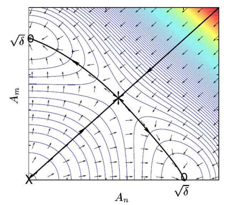
The behavior of the solution of Eq. (10) can be explicitly visualized for the case of two modes (the generalization to more modes is straightforward). The corresponding stationary points of the two nonlinear coupled equations can be found analytically and their stability can be determined through the evaluation of the Jacobian matrix [26]. As the dynamical behavior of the system depends on the sign of the parameter we identify, from Eq. (10), that if the only stationary point is the origin, corresponding to the absence of any oscillation. For this set of parameters the nanowire is at rest in some static configuration determined only by the constant tunneling rates and . On the other hand, if the origin becomes unstable and three more stationary points appear: a saddle point at () and two stable points at () and (). These two new stable points represent oscillating states with finite amplitude and frequency or respectively. Which of these two will be reached by the system depends on the initial conditions as shown in Fig. 6.
The conditions defines the onset of the shuttle instability. From the solution to Eq. (10) with it is possible to find the expression for the threshold electric field above which the instability starts to develop, . Further analysis of Eq. (10) indicates that once the instability for a certain number of vibrational modes is established, the system evolves in such a way that only one of the unstable modes reaches the new stationary state, characterized by steady amplitude oscillations, i.e. the limit cycle. It is also found that the selection of the surviving mode is determined by the initial conditions as the mode which initially has the largest displacement from the origin (that is from the static equilibrium state) maintains its separation from the other modes and evolves into the limit cycle. This can be understood as trajectories in the amplitude space cannot cross, a result that can be analytically generalized to an arbitrary number of modes by studying the asymptotic behavior of the solutions of Eq. (10) [35].
It is worth to remark that the symmetry between the modes that characterizes Fig. 6 is actually broken if higher order (in and ) corrections to become relevant or if the dissipation affects each mode in a different way. Then each mode will have its own and, in general, the selection of the surviving mode may not only depend on the size of the initial displacements from the static equilibrium point.
In order to check the results obtained by the analysis of Eq. (10), one can also compare them to the numerical solution of the “full” equations of motion, Eq. (8). The comparison for a given choice of initial conditions is shown in Fig. 7.

Since the frequencies of the different modes are not commensurable, i.e. they are not integer multiples of the fundamental mode, the initial motion of the nanowire is not characterized by a sharply defined periodicity as can be seen in the lower left panel of Fig. 7. However, when the system reaches the final stationary state and only the mode (which initially had the largest deviation away from static equilibrium) has a non-zero amplitude, its oscillations are clearly periodic with frequency . Similar figures with modes or having finite amplitudes can be obtained by changing the initial conditions.
Note that the numerical analysis of Eq. (8) is not necessarily limited by the requirement that the oscillation amplitude be kept small with respect to the tunneling length. Fig. 7, for instance, suggests that the selective evolution promoted by the simultaneous instability of many vibrational modes can characterize also the “large amplitudes” regime.
II.4 Geometrical scanning of the flexural modes by STM tip displacement
The theoretical study described in the previous section suggests that the development of the shuttle instability in an extended object, such as a suspended nanowire, induces a selective evolution of its many mechanical degrees of freedom. It should be stressed however, that the results presented in Ref. [35] provide more a theoretical demonstration of this selectivity rather than an experimental procedure to control it. The prime reason for this is that the analysis involves the separate choice of initial conditions for each vibrational mode, an operation that cannot be performed experimentally. However, the device considered can still be used to accurately detect the instability of the survivor mode, as the shuttling current is proportional to the mechanical frequency once the system reaches the stable limit cycle [9]. Thus, by measuring the current, we are able to tell which vibrational mode has become unstable.
Besides this, the question of finding a practical procedure to select single vibrational modes through the shuttle instability naturally arises. A possible way to do this was suggested in Ref. [36], by generalizing some of the features of the system considered in Refs. [21, 32, 35]. In this work the tip of the STM is specified in a generic position along the nanowire axis and is no longer fixed above the wire’s midpoint. Under these circumstances the coupling is affected by the shape profiles of the eigenmodes at point (see Eq. (4)).
Ref. [36] also considers the effects of dissipation in the studied device to greater detail than what has been presented in the previous sections. Damping of oscillations in solids can be caused by many different microscopic mechanisms and in general it is impossible to formulate a theory that is able to describe all of them from first principles with arbitrary accuracy. In most cases it is even difficult to accurately determine which is the dominant mechanism for dissipation. For example, certain dissipative processes that can be neglected in bulk materials can be enhanced in nano-devices due to the increased surface-to-volume ratio [37]. To account for these considerations Ref. [36] analyzes not only the usual “viscous” damping term but also considers the Zener theory of dissipation for the standard linear solid [38].
The Zener model provides a simple approach that goes a step beyond the ordinary elasticity theory. According to Hooke’s law, the stress and strain fields, i.e. the macroscopic variables that characterize the mechanical state of a solid, are connected by a simple proportionality relation, such that any change in the former reflects itself instantaneously as a change in the latter and vice versa. In the Zener theory, it is instead assumed that these quantities need a finite relaxation time, and respectively, to reach their equilibrium value. This is a consequence of the internal processes that dissipate energy during any modification of the mechanical state of the solid. For the case of periodic variations of the stress and strain with frequency , the following nonlinear frequency-dependent expression for the -factor can be derived from the Zener theory,
| (12) |
Here, and is the difference between the “unrelaxed” and “relaxed” values of the Young’s modulus [38], in effect a measure of the degree of non-elasticity of the body.
In Ref. [36] a classical description of the system depicted in Fig. 1 was formulated where the tunneling process that charges the nanowire and makes it sensitive to the electrostatic force is a stochastic process. As such, the normal mode amplitudes and conjugated momenta are also stochastic variables and we define probability densities for them when the nanowire is charged and when it is neutral . The evolution of these objects is determined by a generalized Boltzmann equation where the “collisional integral” is replaced by tunneling terms following the approach used in Ref. [39],
| (13) | ||||
| (14) |
The behavior of the system is described by the dynamical variables obtained by averaging the mode amplitudes and conjugated momenta over and : .
The possibility of having a shuttle instability in the weak electromechanical coupling regime is investigated by linearizing the equations of motion for the averaged dynamical variables around the static equilibrium position where the fundamental solutions have the form . The condition for instability of the static configuration of the -th mode can then be expressed as, . For a given quality factor (that is, for a given amount of dissipation), the exponent for each mode can be plotted as a function of the two experimentally accessible parameters: the tunneling rate between the STM tip and the nanowire in the static configuration and the position of the STM tip along the wire axis. The result of this analysis is plotted in Fig. 8 for the case of viscous dissipation () and in Fig. 8 for the case of internal dissipation.


The two plots, Fig. 8 and 8, do not show any qualitative difference. In both cases one can distinguish sets of parameters (, ) for which only one mode is unstable and sets for which two or more modes are unstable. This fact suggests a general way to express the condition for shuttle instability for other types of mechanical degrees of freedom and dissipative processes, , where the real part of is given by,
| (15) |
III Magnetic field induced NEM coupling
In the previous sections we have shown that NEM-SET shuttle structures
can be used to significantly alter the electronic and mechanical
characteristics of the discussed system. In what follows, we will
consider further the case of suspended nanowire structures and show
that these can also be made to mechanically oscillate through the
introduction of external magnetic fields. Due to the effective induced
electron-vibron coupling of these devices novel physical phenomena are
predicted as presented below.
Although suspended nanowires can be viewed as a particular realization of a NEM-SET shuttle structure, specific nanoelectromechanical operation is expected as a result of strong elongation of the movable part of these devices. This comes about as the very large aspect ratios in these systems affect both the mechanics of the flexural vibrations and the electrodynamics of the electronic current flow. Elongation of a suspended wire, or alternatively diminishing its cross-section, will make the wire more flexible and hence more sensitive to external mechanical perturbations. This will in turn make quantum effects more pronounced due to the larger amplitude of the wire’s zero point flexural vibrations. Utilizing this, new types of NEM coupling can be achieved through the induced electron-vibron interaction caused by, e.g., externally applied magnetic fields. This coupling specifies the Lorentz force acting on the wire, and for case of mechanically oscillating wires, also the electromotive force on the electrons which counteracts the motion causing the vibrations. Since the flexibility of the wire increases with its aspect ratio, and the Lorenz force is directly proportional to the length of the wire, significant inductive NEM coupling can be achieved as a result of strong electrical current concentrations in wires of nanosized cross-section.
In comparison to the nanoelectromechanics considered in the previous parts of this paper — where the tuning of the NEM performance was achieved through the coupling of an external electric field to the local charge concentration — we here show that similar results can be achieved if external magnetic fields coupled to the electronic current are instead used. The effects of this type of NEM coupling on a suspended nanowire of length and cross-section , carrying a current in a transverse magnetic field is described through the induced deflection of the wire, . From standard elasticity theory one finds that where with the current density and the Young’s modulus of the wire. For suspended nanowires of length 1 m we estimate that such deflections can be as large as 0.1-1 nm, which can crucially affect the electronic tunneling through such mesoscopic NEM structures. Quantum coherence in the flexural vibrations of the wire may, as such, affect the electronic transport in non-trivial ways if the area ( is the zero point amplitude of oscillation of the wire) available for penetration of the external magnetic field is comparable to the flux quantum. For the realistic case of a vibrating carbon nanotube, such quantum coherent nanoelectromechanics can be achieved for magnetic fields of the order of a few tens of tesla, corresponding to present state of the art experimental achievements. In the following sections two examples of the above discussed inductive nanoelectromechanics will be presented. The new physics of entanglement of resonantly tunneling electrons with nanowire quantum vibrations will be presented in the Section III.1, whereas the possibility to pump nanovibrations by a supercurrent flowing through a suspended nanowire is discussed in Section III.2.
III.1 Quantum mechanically induced electronic Aharonov-Bohm interference
Quantum fluctuation of the nanowire bending modes is a feature which must be taken into account while considering the effects of quantum coherence in the vibration dynamics of a suspended nanowire based tunneling device (see Fig. 9).

This implies that geometrical constraint for the electrons, set by wire geometry, will no longer localize them to the 1-dimensional conducting wire, but will be also imply certain delocalization in the direction transverse to the wire axis. Such change of the dimensionality opens up the possibility for quantum interference effects in the electronic tunneling over the leads if an external magnetic field, , is applied. As a result, a finite magnetoconductance of the 1D vibrating wire occurs as a manifestation of nanomechanical quantum coherence effects [41].
The voltage-biased suspended nanowire structure shown in Fig. 9 was first analyzed in Ref. [41] for the case of nonresonant electronic transmission through the wire. Considering the electronic Fermi level to be far from the energy levels of the quantized longitudinal motion of the electrons in the wire, the authors used perturbation theory with respect to the tunnel barrier transmission, , to calculate the current and conductance through the system. To second order in this expansion, the effective Hamiltonian coupling the electrons in the two leads through the virtual energy level of the wire can be shown to be of the form,
| (16) |
Here, electrons in the leads are described by the first term while the fundamental mode of the flexural vibrations11 1 For simplicity, only the fundamental mode is considered in this analysis. is described by its harmonic oscillator Hamiltonian (the second term in Eq. (16)). The additional phase factor connected with the tunneling electrons (third term in (16)) describes the magnetic field dependent phase which the electrons acquire between the two sequential tunneling events at the ends of the wire. The specifics of this term for the problem considered is that the electronic phase is not a c-number, but an operator acting in the quantum vibrational space.
As the effective coupling strength for the tunneling electrons experiences quantum fluctuations so does the number of different tunneling channels. Since these channels obey quantum nanomechanical dynamics, we obtain a typical picture of entanglement between the quantum nanomechanical and electronic degrees of freedom. The outcome of this is that new polaronic states (referred to as “swinging states” in Ref. [41]) are formed in the wire as a result of this entanglement, and charge transport can now be viewed as electronic transmission through these intermediate states. It is interesting to note that the strength of such polaronic coupling is determined by magnetic flux and can thus be tuned by the external magnetic field.
From the effective tunneling Hamiltonian, Eq. (16), the electric current over the voltage-biased leads can easily be calculated. What is new in this analysis is that the matrix elements corresponding to electronic tunneling are now described through operators in the vibrational space of the wire, something that needs to be considered when tracing out the electronic and vibrational phase space. The resulting expression for the current is presented in Eq. (17),
| (17) | ||||
Here, is the zero field conductance, is the electric charge and the oscillating nanowire is assumed to be in thermal equilibrium with the environment, described through , the probability of finding the oscillator in a quantum state with energy at a temperature ( and is the frequency of oscillation of the nanowire). The electron-vibron coupling is expressed through the coupling constant , which scales linearly with the magnetic field. Finally are the Fermi functions for the left and right lead kept at chemical potential respectively with the bias voltage.

The above expression represents contributions to the current from a number of different inelastic tunneling channels, , together with the elastic channel. Analyzing Eq. (17) one finds that the destructive Aharonov-Bohm interference to the elastic channel caused by the quantum fluctuations in the magnetic flux (proportional to the area enclosed by the vibrating quantum wire) is compensated by the additional inelastic tunneling channels. These inelastic channels increase the electronic transport through the system, and hence compensates the effect of the quantum suppression in the elastic channel. The influence of these two effects on the total transport depends on the extent to which the inelastic channels are permitted by the Pauli principle, which limits the electron-vibron energy transfer. The corresponding energy diagram for the different electronic tunneling channels is presented in Fig. 10.
Neglecting with the Fermi statistics of the electrons (high temperature limit), the restrictions imposed by the summation over the possible inelastic tunneling channels in Eq. (17) disappears, and the expression for the conductance exactly coincides with the transmission through the non-vibrating wire (see Eq. (18)). In the low temperature limit however, the result of the abovementioned quantum mechanical suppression of the elastic channel and the Pauli restrictions on some of the inelastic channels is the appearance of a finite magnetoconductance. As a result, the strongest effects of the predicted quantum magnetoconductance occurs in the low voltage, low temperature limit: . At higher energies, the Pauli restrictions become less important, and these effect only give corrections to the conductance as compared to the non-vibrating wire. Mathematically the asymptotic limits to the magnetoconductance are found as,
| (18) |
which can also be seen in Fig. 11. Similar results of quantum mechanical effects on the conductance have been reported for the case of ballistic electron transport through a carbon nanotube encapsulating a single movable fullerene scatterer [42] (see also Ref. [43] for a resonant tunneling treatment of a similar system).
The effects of the quantum suppression of the low energy tunneling processes outlined above are only visible in the low temperature, low bias voltage limit and are hence hard to verify experimentally. If, however, the electrical current is instead considered these effects are indeed visible also at higher temperatures and voltages. This can be understood as the Pauli restrictions on the inelastic tunneling channels affect only the low energy electrons (low bias voltage). Thus, the low voltage current is reduced from the non-vibrating ohmic current, , by an amount that is given by the extent to which the elastic channel is suppressed (which in turn depends on the magnetic field). As the bias voltage is increased the inelastic tunneling channels are opened and the current increases accordingly. However, a further increase in the bias voltage when the conditions are fulfilled will not be affected by the Pauli restrictions due to the large energy scales of the electrons. As a result, these effects are displayed as a temperature- and bias voltage-independent current deficit, as compared to the non-vibrating wire, as recently reported in Ref. [40],
| (19) |
The effect of the quadratic magnetic field dependence on the current deficit can be experimentally observed by extrapolating the high voltage asymptotes of the curves to the limit (see Fig. 11). For realistic parameters, we estimate that these effects should be observable for bias voltages 30 V and currents 3 pA in magnetic fields of 20 T.

By exploiting the equilibrium distribution of the flexural vibrations, in Eq. (17), we have neglected with the non-equilibrium effects which can be stimulated in the vibronic subspace due to the coupling to the current carrying electrons. This assumption is valid if the internal relaxation of the vibronic subsystem is strong compared to the excitation strength set by the electronic emission of vibrons. If this is not the case, such electron-vibron coupling cannot be ignored, even if the electronic tunneling is small. In order to account for the mutual electron-vibron dynamics, one should evaluate the evolution of the density matrix operating on both the vibronic and electronic subspaces, and, using this density matrix, calculate the vibronic contribution to the current as well as the electron-vibron contribution to the Lorentz force. This analysis was recently performed in Ref. [40], where it was shown that the stationary density matrix can be found as a result of a balance between the electron assisted emission and absorption of vibrons. The equation for the stationary reduced density matrix, , of the electron-vibron subspace takes the form,
| (20) | ||||
Here, are operators that take into account the electron-vibron coupling and is the first two terms in Eq. (16). Also, the average Lorentz force (21a) and momentum (21b) on the wire can be found by multiplying Eq. (20) with the deflection and momentum operators and tracing out the nanowire’s degrees of freedom,
| (21a) | |||
| (21b) | |||
In Ref. [40] it was shown that although each inelastic electronic tunneling channel (see Eq. (17)) is significantly renormalized by the non-equilibrium of the vibronic subsystem, the total high voltage limit, , to the current is still given by Eq. (19). Furthermore, any corrections to this expression from the thermal environment was shown to decay exponentially in this limit for all relaxation strengths in the vibronic subsystem.
III.2 Nanoelectromechanics of suspended nanowire superconducting weak link
Superconducting ordering in the electronic subsystem qualitatively changes the electromechanical coupling in the suspended nanowire based NEM tunneling devices considered so far. If the electronic subsystem of the leads in Fig. 9 undergoes a superconducting phase transition a new type of electronic coupling between the leads occurs. This coupling allows for the possibility of coherent tunneling of a pair of electrons (a Cooper pair), forming a superconducting condensate of electrons in each of the two leads. As the process of Cooper pair tunneling is a dissipationless ground state property of the superconductors, a finite dc current over the leads will be present even at zero bias voltage (the dc Josephson effect). If instead a finite dc bias is applied an alternating Josephson current is set up over the leads, representing the tunneling response of the junction to the bias, whose zero average value guarantees that no electric power is absorbed from the voltage source. The frequency of these current oscillations is set by the energy gained by a single Cooper pair during its transition between the superconducting leads: (the ac Josephson effect).
If now the tunneling Cooper pairs are coupled to the mechanical vibrations of the suspended nanowire, an electromotive force is induced due to the presence of the external magnetic field causing the vibrations22 2 The inductive coupling between flexural wire vibrations and the supercurrent flow in a SQUID loop was considered in Refs. [54, 55, 56].. The work done by this force on a tunneling Cooper pair renormalizes the total energy gained by it and hence changes the frequency of the Josephson oscillations. On the other hand, the mechanical vibrations of the nanowire are affected by the Lorentz force which oscillates in time due to the ac variations of the Josephson current in the wire. From these considerations a set of equations determining the Josephson frequency renormalization and the mechanical motion of the wire were derived in Ref. [44]. These equations were found by considering the Andreev level formation in the NEM-superconducting weak link in the low tunnel barrier transparency limit (see also Appendix A) and are fully consistent with the qualitative picture describe above. Using the dimensionless coordinates , and for the wire’s deflection coordinate, driving force and phenomenological damping respectively these equation are,
| (22a) | |||
| (22b) | |||
In (22), is the dimensionless applied bias voltage and the driving force . Eq. (22) is thus the equation of motion for the deflection coordinate of the wire which is driven by a force proportional to a term reminiscent of the ac Josephson current, . Note however, that as the wire moves in the magnetic field it induces an electromotive force proportional to the time rate of change of the deflection coordinate, which counteracts the motion causing the vibration. This term is given by the second argument in Eq. (22b) (see Ref. [44] for details), and is responsible for the characteristic resonant phenomena described below.
Numerical simulations of Eq. (22) shows that for small driving forces (low magnetic fields) the system will achieve resonant conditions only at the eigenfrequency of the fundamental mode of the wire , see Fig. 12(a). For larger driving forces however, also parametric excitations can be achieved, Fig. 12(b).
Furthermore, the amplitude of these modes is initially seen to be an increasing function of the magnetic field strength, but eventually saturates at some critical driving force , Fig. 13. To explain these phenomena we derive two stability equations for the amplitude and phase of the vibrating nanowire which well describe the onset and saturation of finite vibrations at resonant conditions. These equations also show that for the system considered there exists a window of bistability in the vibrational amplitude around the resonance peaks.
Being that the voltage source pumps energy into the oscillating nanomechanical system, it can be shown by direct integration of the equation of motion that at resonant conditions a finite dc current, , is set up over the system. This comes about as the mechanical energy of the nanowire is a constant of time at resonant conditions, hence any pumping of the system at these conditions will lead to an energy transfer through it, proportional to the real damping coefficient . As such, the resonant dc current can be shown to scale as,
| (23) |
where time-average rate of change of the deflection coordinate, , behaves phenomenologically equivalent to the deflection coordinate. As such, we predict that the system considered should exhibit both negative and positive magnetoresistance as the current is first an increasing function of the magnetic field (increasing vibrational amplitude) but falls off as once the driving force reaches the critical value which indicates the onset of the bistability in the vibrational amplitude (see inset Fig. 13).
Also, we have shown that the bistability region around the resonance peaks can be utilized to directly probe the underlying quantum mechanics of the system. As was mentioned above, close to resonance conditions the system exhibits a mechanical bistability, i.e. two dynamically stable solutions of oscillation can be found for the same bias voltage but with different vibrational amplitudes. Which of the two stability point the system will correspond to will in general depend on initial conditions, however, by applying finite voltage pulses in time one can move the system between the two. Consider for example the situation shown in Fig. 13 where the system is initially found at the stable point 1, corresponding to the lower vibrational amplitude (lower current) and the bias voltage is slightly off the parametric resonance. Applying two voltage pulses in time, (i) and (ii), will move the system along the phase space trajectory of the stability point defining it. As the region of bistability is only found within a small window of bias voltage around the resonance peaks, pulse (i) will in this example force the system into the second stability point, which will return the system to the higher stability point, 2, on the up-sweep. As the dc current scales directly with the vibrational amplitude we thus predict that this pulse will result in a measurable current difference to pulse (ii) which will return the system to the initial stability point. Considering realistic parameters we predict that the measurable current difference () 5 nA should be experimentally observable for magnetic fields 20 mT and bias voltages 5 V.
IV Conclusions
Coupling between electrical and mechanical degrees of freedom is the basic mechanism behind the functionality of any nanoelectromechanical system. Such coupling can be achieved in many different ways. In this Review we have focused on the effects of varying the spatial concentration of the electronic charge or current in systems incorporating suspended nanowires as the mechanical element. These structures are particularly interesting to study as they can be used as efficient electromechanical transducers that serve simultaneously as electric weak links for the tunneling electrons and as nanomechanical resonators. This allows one to use the mutual coupling between the electric current oscillations in time and the mechanical vibrations to achieve a highly nonlinear electromechanical coupling if strong driving voltages or magnetic fields are applied. The resulting self-supported nanoelectromechanical dynamics can be maintained through the development of an electromechanical instability, caused either by the shuttle phenomenon (for systems with varying charge concentration) or through resonant pumping of nanovibrations by the electric current flow (in systems with strong current concentration).
In many of the systems considered in this Review, quantum coherence is an essential feature of the discussed nanoelectromechanical operations. For example, we have shown that quantum effects in the electronic subsystem, such as coherent electron transmission through a double barrier structure, can be coupled to the quantum coherence of the mechanical flexural vibrations (Section III.1). The resulting electromechanical entanglement establishes “swinging” polaronic states for the tunneling electrons, which allows the quantum vibrations to be investigated by interferometry. Also, we have shown that the existence of more than one mode of nanomechanical bending of the suspended nanowire, a direct consequence of the spatial extension of the mechanically vibrating element, makes the operation of the NEM device even richer. As an example we mention the multimode shuttle instability discussed in Section II.4 where it was shown that by applying a “local” external probe in the form of current injection from an STM tip the “global” mechanical properties of the system as a whole can be altered. In particular, the competition between the different mechanical modes of vibrations will lead to a self-organization of the shuttle vibrations of the suspended nanowire.
Experimental realization of the phenomena discussed in this Review is an experimentally challenging task. Although NEM-structures based on suspended nanowires have been manufactured by a number of labs [45, 17, 46, 14, 13, 18, 47, 16, 19, 22, 48], the need for strong external magnetic fields and applied voltages offers a real experimental challenge. Another obstacle to experimental realization of these systems is damping of the nanomechanical vibrations. If, for example, the mechanical damping is too large, then the voltage threshold required for the onset of the electromechanical instability may well exceed the thermal limit, set by Joule heating of the system, and the system might burn [49]. However, for the NEM systems considered here typical experimental parameters such as quality factors of the order and bias voltages of order 1 V the suggested multimode shuttling and superconducting pumping of nanovibrations should be experimentally observable. The effects of the interferometry of the quantum nanovibrations discussed here do nevertheless demand the presently best achievable experimental conditions.
In this Review we have discussed the coupling of mesoscopic electrons to nanomechanical radio frequency vibrations. It is interesting to compare this to how mesoscopic electrons couple to external electromagnetic fields of much higher frequencies. Such coupling has been been shown to result in a number of interesting non-equilibrium mesoscopic phenomena in both normal [50, 51] and superconducting [52, 53] mesoscopic structures if the microwave photon energy is comparable to the electronic energy-level spacing. The much lower mechanical frequencies of NEMS devices, on the other hand, can easily be tuned to match the smaller electronic energy scales that characterize the widths (due to tunneling) of electronic energy levels, the applied bias voltage, or the frequency of Rabi oscillations in the population of energy levels. The fact that electrons in mesoscopic systems can couple to oscillations corresponding to such very different energy scales, makes it tempting to speculate that mesoscopic electrons might be used for making microwave-mechanical transducers by simultaneously coupling them to both electromagnetic and nanomechanical degrees of freedom. If such an electron-mediated microwave-mechanical coupling is possible in principle, one may wish to consider quantum coherence effects in structures where both electromagnetic, mechanical and electronic degrees of freedom have been quantum mechanically entangled. The extent to which such speculations are realistic is an open question which we leave for future research in the exciting field of nanoelectromechanics to answer.
Acknowledgments This work was supported in parts by the Swedish VR and SSF, by the Faculty of Science at the University of Gothenburg through its “Nanoparticle” Research Platform and by the Korean WCU program funded by MEST through KOSEF (R31-2008-000-10057-0).
Appendix A Derivation of the expression for the force on the pumped nanomechanical system
Consider the Hamiltonian, , for the electronic subsystem of the pumped Josephson vibrations of the suspended nanotube, Eq. (1) in Ref. [44],
| (24) |
In (24), [] are two-component Nambu spinors, are the Pauli matrices in Nambu space and the deflection of the tube is given by , where is the dimensionless, normalized profile of the fundamental bending mode and determines the amplitude of vibration. The potential describes the barrier between the nanotube and the bulk superconducting electrodes where the gap parameter is and is the phase difference across the junction. As indicated in Ref. [44] a gauge transform, with , shifts the dependence of the vector potential induced by the nanotube deflections from the kinetic part of the Hamiltonian to the phase differences over the leads, .
Suppose now that we have an eigenstate of the system, , such that where is the ground state of the system corresponding to energy and is some state orthogonal to the ground state. To be able to evaluate the force on the system with respect to the ground state we need to show that is small, which can be done by expanding it in a complete set of eigenstates of the Hamiltonian, . Inserting this form into the Schrödinger equation and multiplying from the left with the state , we find that the amplitudes can be expressed as,
| (25) |
To evaluate this further we need to find and expression for the term in the nominator of Eq. (25) which can be done by considering the time derivative of the eigenstate solution and evaluating the matrix elements of this equation with . Performing this analysis we find that we can express Eq. (25) as,
| (26) |
As the only time-dependence of the transformed Hamiltonian is found in the phase difference over the leads we identify that the nominator of this expression is proportional to the bias voltage, , whereas the denominator is the spacing of the energy levels in the systems, . Hence, for the system considered , we can safely evaluate the expression for the force with respect to the fixed-phase ground state .
The force on the wire is then found by evaluating the expectation value of the force operator which can easily be shown to be , where is the ground state energy as given in Ref. [44]. Similarly the Josephson current can be shown to be and we recover the total expression for the force on the oscillating wire as given in Eq. (22).
References
- [1] R. P. Andres, T. Bein, M. Dorogi, S. Feng, J. I. Henderson, C. P. Kubiak, W. Mahoney, R. G. Osifchin, and R. Reifenberger, Science 272, 1323 (1996).
- [2] E. S. Soldatov, V. V. Khanin, A. S. Trifonov, D. E. Presnov, S. A. Yakovenko, G. B. Khomutov, C. P. Gubin, and V. V. Kolesov, Pisma Zh. Eksp. Teor. Fiz. 64, 510 (1996) [JETP Lett. 64, 556 (1996)].
- [3] H. Park, J. Park, A. K. L. Lim, E. H. Anderson, A. P. Alivisatos, and P. L. McEuen, Nature 407, 57 (2000).
- [4] D. V. Scheible and R. H. Blick, New J. Phys. 84, 4632 (2004).
- [5] A. Erbe, C. Weiss, W. Zwerger, and R. H. Blick, Phys. Rev. Lett. 87, 096106 (2001).
- [6] M. D. LaHaye, O. Buu, B. Camarota, and K. C. Schwab, Science 304, 74 (2004).
- [7] A. Naik, O. Buu, M. D. LaHaye, A. D. Armour, A. A. Clerk, M. P. Blencowe, and K. C. Schwab, Nature 443, 193 (2006).
- [8] R. G. Knobel and A. N. Cleland, Nature 424, 291 (2003).
- [9] L. Y. Gorelik, A. Isacsson, M. V. Voinova, B. Kasemo, R. I. Shekhter, and M. Jonson, Phys. Rev. Lett. 80, 4526 (1998a).
- [10] R. I. Shekhter, Y. Galperin, L. Y. Gorelik, A. Isacsson, and M. Jonson, J. Phys: Condens. Matter 15, R441 (2003).
- [11] R. I. Shekhter, L. Y. Gorelik, M. Jonson, Y. M. Galperin, and V. M. Vinokur, J. Comput. Theor. Nanosci. 4, 860 (2007).
- [12] K. Flensberg, New J. Phys. 8, 5 (2006).
- [13] S. Sapmaz, Y. M. Blanter, L. Gurevich, and H. S. J. van der Zant, Phys. Rev. B 67, 235414 (2003).
- [14] M. Poot, B. Witkamp, M. A. Otte, and H. S. J. van der Zant, Phys. Status Solidi B 244, 4252 (2007).
- [15] V. Sazonova, Y. Yaish, H. Ustunel, D. Roundy, T. A. Arias, and P. L. McEuen, Nature 431, 284 (2004).
- [16] B. Witkamp, M. Poot, and H. S. J. van der Zant, Nano Lett. 6, 2904 (2006).
- [17] A. K. Hüttel, M. Poot, B. Witkamp, and H. S. J. van der Zant, New J. Phys. 10, 095003 (2008).
- [18] S. Sapmaz, P. Jarillo-Herrero, Y. M. Blanter, C. Dekker, and H. S. J. van der Zant, Phys. Rev. Lett. 96, 026801 (2006a).
- [19] B. J. LeRoy, S. G. Lemay, J. Kong, and C. Dekker, Nature 432, 371 (2004a).
- [20] R. I. Shekhter, Zh. Eksp. Theor. Fiz. 63, 1400 (1972) [Sov. Phys. JETP 36, 747 (1973)]; I. O. Kulik and R. I. Shekhter, Zh. Eksp. Theor. Fiz. 68, 623 (1975) [Sov. Phys. JETP 41, 308 (1975)]; D. V. Averin and K. K. Likharev, J. Low Temp. Phys. 62, 345 (1986).
- [21] L. M. Jonsson, L. Y. Gorelik, R. I. Shekhter, and M. Jonson, Nano Lett. 5, 1165 (2005).
- [22] B. J. LeRoy, S. G. Lemay, J. Kong, and C. Dekker, Appl. Phys. Lett. 84, 4280 (2004b).
- [23] W. Izumida and M. Grifoni, New J. Phys. 7, 244 (2005).
- [24] A. Zazunov, D. Feinberg, and T. Martin, Phys. Rev. B 73, 115405 (2006).
- [25] L. D. Landau and E. M. Lifshitz, Theory of elasticity, Pergamon Press, Oxford (1986), 3rd ed.
- [26] S. Strogatz, Nonlinear dynamics and chaos: with applications to physics, biology, chemistry and engineering, Perseus Books, Cambridge (2001).
- [27] R. Lifshitz and M. L. Roukes, Phys. Rev. B 61, 5600 (2000).
- [28] Z. Hao, A. Erbil, and F. Ayazi, Sensor Acutator. 109, 156 (2003).
- [29] F. R. Blom, S. Bouwstra, M. Elwenspoek, and J. H. J. Fluitman, J. Vac. Sci. Technol. B 10, 19 (1992).
- [30] S. Perisanu, P. Vincent, A. Ayari, M. Choueib, and S. T. Purcell, Appl. Phys. Lett. 90, 043113 (2007).
- [31] A. Isacsson, L. Y. Gorelik, M. V. Voinova, B. Kasemo, R. I. Shekhter, and M. Jonson, Physica B 225, 150 (1998).
- [32] L. M. Jonsson, L. Y. Gorelik, R. I. Shekhter, and M. Jonson, New J. Phys. 9, 90 (2007).
- [33] D. Fedorets, L. Y. Gorelik, R. I. Shekhter, and M. Jonson, Phys. Rev. Lett. 92, 166801 (2004).
- [34] T. Novotny, A. Donarini, and A.-P. Jauho, Phys. Rev. Lett. 90, 256801 (2003).
- [35] L. M. Jonsson, F. Santandrea, L. Y. Gorelik, R. I. Shekhter, and M. Jonson, Phys. Rev. Lett. 100, 186802 (2008).
- [36] F. Santandrea, arXiv:0902.4184 (unpublished).
- [37] D. W. Carr, S. Evoy, L. Sekaric, H. G. Craighead, and J. M. Parpia, Appl. Phys. Lett. 75, 920 (1999).
- [38] A. S. Nowick and B. S. Berry, Anelastic relaxation in crystalline solids, Academic Press, New York (1972).
- [39] A. D. Armour, M. P. Blencowe, and Y. Zhang, Phys. Rev. B 69, 125313 (2004).
- [40] G. Sonne, arXiv:0901.4017 (unpublished).
- [41] R. I. Shekhter, L. Y. Gorelik, L. I. Glazman, and M. Jonson, Phys. Rev. Lett. 97, 156801 (2006).
- [42] G. Sonne, L. Y. Gorelik, R. I. Shekhter, and M. Jonson, Europhys. Lett. 84, 27002 (2008a).
- [43] I. V. Krive, R. Ferone, R. I. Shekhter, M. Jonson, P. Utko, and J. Nygård, New J. Phys. 10, 043043 (2008).
- [44] G. Sonne, R. I. Shekhter, L. Y. Gorelik, S. I. Kulinich, and M. Jonson, Phys. Rev. B 78, 144501 (2008b).
- [45] S. Etaki, M. Poot, I. Mahboob, K. Onomitsu, H. Yamaguchi, and H. S. J. van der Zant, Nat. Phys. 4, 785 (2008).
- [46] P. Poncharal, Z. L. Wang, D. Ugarte, and W. A. de Heer, Science 283, 1513 (1999).
- [47] S. Sapmaz, P. Jarillo-Herrero, Y. M. Blanter, and H. S. J. van der Zant, New J. Phys. 7, 243 (2006b).
- [48] D. R. Koenig, E. M. Weig, and J. P. Kotthaus, Nat. Nanotechnol. 3, 482 (2008).
- [49] J. Svensson, Private commun.
- [50] A. Grincwajg, L. Y. Gorelik, V. Z. Kleiner, and R. I. Shekhter, Phys. Rev. B 52, 12168 (1995).
- [51] L. Y. Gorelik, F. A. Maaø, R. I. Shekhter, and M. Jonson, Phys. Rev. Lett. 78, 3169 (1997).
- [52] L. Y. Gorelik, V. S. Shumeiko, R. I. Shekhter, G. Wendin, and M. Jonson, Phys. Rev. Lett. 75, 1162 (1995).
- [53] L. Y. Gorelik, N. I. Lundin, V. S. Shumeiko, R. I. Shekhter, and M. Jonson, Phys. Rev. Lett. 81, 2538 (1998b).
- [54] M. P. Blencowe and E. Buks, Phys. Rev. B 76, 014511 (2007).
- [55] E. Buks and M. P. Blencowe, Phys. Rev. B 74, 174504 (2006).
- [56] E. Buks, E. Segev, S. Zaitsev, B. Abdo, and M. P. Blencowe, Europhys. Lett. 81, 10001 (2008).